Report an Error


NVIDIA Tesla P100 DGXS
- Graphics Processor
- GP100
- Cores
- 3584
- TMUs
- 224
- ROPs
- 96
- Memory Size
- 16 GB
- Memory Type
- HBM2
- Bus Width
- 4096 bit
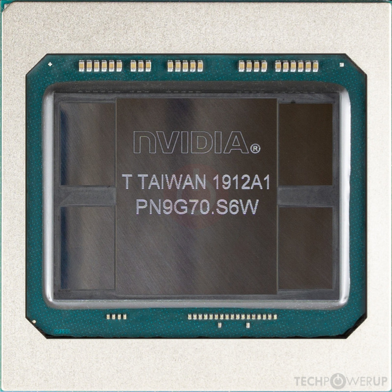
GPU
The Tesla P100 DGXS was a professional graphics card by NVIDIA, launched on April 5th, 2016. Built on the 16 nm process, and based on the GP100 graphics processor, the card supports DirectX 12. The GP100 graphics processor is a large chip with a die area of 610 mm² and 15,300 million transistors. It features 3584 shading units, 224 texture mapping units, and 96 ROPs. NVIDIA has paired 16 GB HBM2 memory with the Tesla P100 DGXS, which are connected using a 4096-bit memory interface. The GPU is operating at a frequency of 1328 MHz, which can be boosted up to 1480 MHz, memory is running at 715 MHz.
Its power draw is rated at 300 W maximum. This device has no display connectivity, as it is not designed to have monitors connected to it. Tesla P100 DGXS is connected to the rest of the system using a PCI-Express 3.0 x16 interface.
Its power draw is rated at 300 W maximum. This device has no display connectivity, as it is not designed to have monitors connected to it. Tesla P100 DGXS is connected to the rest of the system using a PCI-Express 3.0 x16 interface.
Graphics Processor
Graphics Card
- Release Date
- Apr 5th, 2016
- Generation
-
Tesla Pascal
(Pxx)
- Predecessor
- Tesla Maxwell
- Successor
- Tesla Volta
- Production
- End-of-life
- Bus Interface
- PCIe 3.0 x16
Relative Performance
Based on TPU review data: "Performance Summary" at 1920x1080, 4K for 2080 Ti and faster.
Performance estimated based on architecture, shader count and clocks.
Clock Speeds
- Base Clock
- 1328 MHz
- Boost Clock
- 1480 MHz
- Memory Clock
-
715 MHz
1430 Mbps effective
Memory
- Memory Size
- 16 GB
- Memory Type
- HBM2
- Memory Bus
- 4096 bit
- Bandwidth
- 732.2 GB/s
Render Config
- Shading Units
- 3584
- TMUs
- 224
- ROPs
- 96
- SM Count
- 56
- L1 Cache
- 24 KB (per SM)
- L2 Cache
- 4 MB
Theoretical Performance
- Pixel Rate
- 142.1 GPixel/s
- Texture Rate
- 331.5 GTexel/s
- FP16 (half)
- 21.22 TFLOPS (2:1)
- FP32 (float)
- 10.61 TFLOPS
- FP64 (double)
- 5.304 TFLOPS (1:2)
Board Design
- TDP
- 300 W
- Suggested PSU
- 700 W
- Outputs
- No outputs
- Power Connectors
- None
Graphics Features
- DirectX
- 12 (12_1)
- OpenGL
- 4.6
- OpenCL
- 3.0
- Vulkan
- 1.3
- CUDA
- 6.0
- Shader Model
- 6.0
GP100 GPU Notes
| NVENC: 6th Gen NVDEC: 3rd Gen PureVideo HD: VP8 VDPAU: Feature Set H |
Apr 26th, 2024 12:12 EDT
change timezone
Latest GPU Drivers
New Forum Posts
- XFX RX470 8GB no video and error 43 (28)
- The TPU UK Clubhouse (24788)
- Secure boot already open help (9)
- im new to throttelstop and i think i messed it up by copying others any hints would be very much aprreciated (4)
- Cs2 Freezing in Rx 580 (5)
- Ghost of Tsushima PC Port !!!! (15)
- The Official Linux/Unix Desktop Screenshots Megathread (699)
- Red Dead Redemption using emu (4)
- Meta Horizon OS (21)
- Old high quality PSU, or semi-old mid-quality PSU? (3)
Popular Reviews
- HYTE THICC Q60 240 mm AIO Review
- MOONDROP x Crinacle DUSK In-Ear Monitors Review - The Last 5%
- Alienware Pro Wireless Gaming Keyboard Review
- Upcoming Hardware Launches 2023 (Updated Feb 2024)
- Thermalright Phantom Spirit 120 EVO Review
- ASUS Radeon RX 7900 GRE TUF OC Review
- FiiO K19 Desktop DAC/Headphone Amplifier Review
- RTX 4090 & 53 Games: Ryzen 7 5800X vs Ryzen 7 5800X3D Review
- NVIDIA RTX 4090: 450 W vs 600 W 12VHPWR - Is there any notable performance difference?
- Sapphire Radeon RX 7900 GRE Pulse Review
Controversial News Posts
- Windows 11 Now Officially Adware as Microsoft Embeds Ads in the Start Menu (126)
- Sony PlayStation 5 Pro Specifications Confirmed, Console Arrives Before Holidays (117)
- NVIDIA Points Intel Raptor Lake CPU Users to Get Help from Intel Amid System Instability Issues (106)
- AMD "Strix Halo" Zen 5 Mobile Processor Pictured: Chiplet-based, Uses 256-bit LPDDR5X (101)
- US Government Wants Nuclear Plants to Offload AI Data Center Expansion (98)
- AMD's RDNA 4 GPUs Could Stick with 18 Gbps GDDR6 Memory (92)
- Developers of Outpost Infinity Siege Recommend Underclocking i9-13900K and i9-14900K for Stability on Machines with RTX 4090 (85)
- Windows 10 Security Updates to Cost $61 After 2025, $427 by 2028 (84)