Monday, March 31st 2025

Report Suggests TSMC's Successful Completion of 2 nm Trial Phase, Cross-facility Mass Production Expected by End of Year
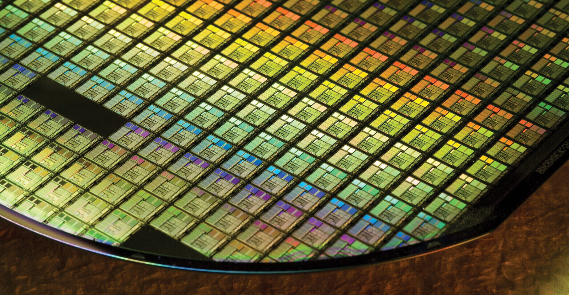
Going back to the start of this year, TSMC's trial run of a cutting-edge 2 nm (N2) node process was reportedly progressing beyond initial expectations. According to industry moles, two flagship fabrication facilities are "optimistically" tipped to pump out 80,000 units per month (by the end of 2025). This cross-facility total figure was linked to TSMC's Baoshan—located near the Northern Taiwanese city of Hsinchu—and Kaohsiung (in the South) plants. The latest regional reports suggest that the aforementioned trial phase was a resounding success, with pleasing results pointing to an "ahead of schedule" transfer to mass production phases. Insiders previously heard about the Kaohsiung production hub's schedule; with mass production set to start by early 2026—according to fresh rumors, revised calendars have a kick-off window repositioned somewhere in late 2025. Apparently a special "2 nm plant expansion ceremony" took place in that location, earlier today.
A noted semiconductor business analyst—Ming-Chi Kuo—reckons that recent 2 nm pilot yields have progressed well over the 60% mark, meaning that the involved foundry teams are more than ready to move onto kicking things into high gear. Taiwan's Economic News Daily anticipates significant financial gains, due to TSMC N2 products already being in high demand: "the quarterly revenue in the second half of the year is expected to reach one trillion yuan (~US$30.1 billion) for the first time, and it is poised to challenge the goal of earning twice the share capital in a quarter and rewrite the record for a single quarter." The local publication claims that TSMC Baoshan's "first batch of production capacity" is fully reserved for Apple, while Kaohsiung will take care of orders for other (i.e. less) important customers.


Sources:
Economic News Daily Taiwan, Wccftech, Chosun Biz, Dan Nystedt Tweet
A noted semiconductor business analyst—Ming-Chi Kuo—reckons that recent 2 nm pilot yields have progressed well over the 60% mark, meaning that the involved foundry teams are more than ready to move onto kicking things into high gear. Taiwan's Economic News Daily anticipates significant financial gains, due to TSMC N2 products already being in high demand: "the quarterly revenue in the second half of the year is expected to reach one trillion yuan (~US$30.1 billion) for the first time, and it is poised to challenge the goal of earning twice the share capital in a quarter and rewrite the record for a single quarter." The local publication claims that TSMC Baoshan's "first batch of production capacity" is fully reserved for Apple, while Kaohsiung will take care of orders for other (i.e. less) important customers.


14 Comments on Report Suggests TSMC's Successful Completion of 2 nm Trial Phase, Cross-facility Mass Production Expected by End of Year
I hope..
if Mr. K. "reckons" it, then it MUST be so.. :roll:Yea well, the thing with those chips is that they don't actually work, but are merely for photo show purposes, and ONLY from a distance (ie no hands-ons), hehehehe :)
With what Nova Lake is proposed to be it may have been necessary (where-as 3nm may have only truly allowed for greater core count on a ccd, 2nm may facilitate higher clocks; perhaps similar to Intel...~6ghz+?).
None of that would have been feasible without production like this going as smoothly as it appears to have (rather than say MP by EOY 2026 for N2P/X/A16 as was previously thought to be the case).
This is what good competition does; it pushes things forward faster (including the leaders in the space), including higher volume production earlier.
But, yeah, I agree. The battle of 2026 CPUs should be quite fascinating; I wonder which variant of 2nm chose for (parts of) Nova. Regardless, sadly, all potentially very expensive given the quick move to that process.
One thing is fo' sho', AM5 is going to have one big last hurrah (similar to 5800x3D), and that's always cool for peeps that may stay on that platform and just upgrade later on (rather than move to say AM6 in ~2028?).
One could argue a 5800x3d (and 5700x3d) did a decent job of lasting through the whole AM5 generation; I wonder if whatever the ultimate 12c x3d will be able to say the same versus general AM6 parts. Maybe!
Using 2nm while still on AM5 certainly doesn't hurt, and again, I think that's pretty rad for the longevity of the platform and it's users' upgrade paths w/o having to switch platforms (even at it's end).
i can see amd picking n3e for the ccd iod won’t be going much smalller, it might get split up sothe npu and gpu are on 3nm to io won’t be made on that tiny node.
crocusnano.com/en/crocus-nano-electronics-has-released-new-generation-non-volatile-memory
- The latest GPUs came out in the last 6 months from Nvidia, AMD, and Intel and all use TSMC N5/N4.
- Every AMD Zen 5 chip is N4P, and obviously Zen 5c on mobile shares a die with Zen 5 so it is N4P as well.
- Qualcomm laptop processors use N4P.
- AMD has announced no new CPUs coming soon. The rest of this year appears to just have refreshes of N4P processors.
- Intel server CPUs use Intel 3 (probably on par with a TSMC N5 node, possibly as good as N4P).
- Zen 6 appears to be coming to market after N2 becomes available.
There are a few N3 products:- The Apple M3 series uses N3B and M4 uses N3E.
- AMD Zen 5c server chiplets use N3-something.
- Intel Lunar Lake and Arrow Lake use N3B. Arrow Lake was promised to Intel 20A so N3B wasn't the first choice.
Lunar Lake and the laptop implementation of Arrow Lake were well-received* but Arrow Lake on desktop has clock speed regressions compared to Arrow Lake, so N3B is not the best node for desktop clock frequencies. N3E, N3P, and N3X will probably do better, but N3E only recently became available to Apple and N2 is on track for early next year so at this rate N3P and N3X will come to market around the same time as N2.*I saw a lot of complaints from commenters that Lunar Lake had too few cores, but I think people who knew what it was and that Arrow Lake was coming soon with more cores were pleased with Lunar Lake.
What's the defect rate per cm^2 of N2?