News Posts matching #7 nm

Return to Keyword Browsing

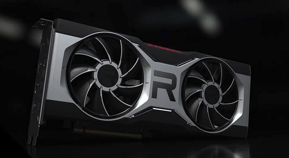
AMD Announces Radeon PRO W6000 Series Professional Graphics Cards Based on RDNA2

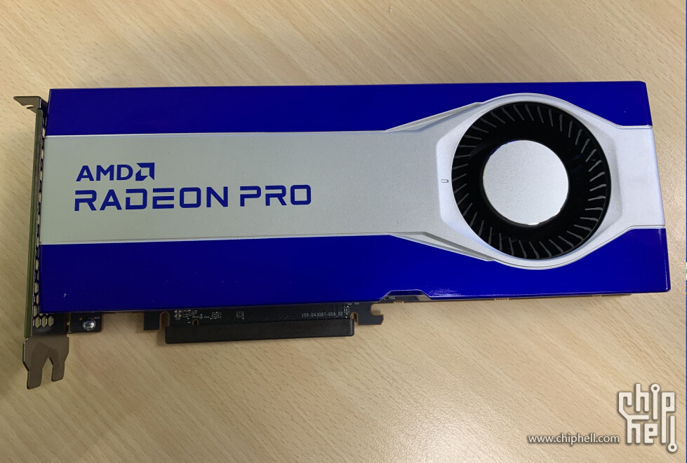
AMD today announced the AMD Radeon PRO W6000 series workstation graphics, delivering exceptional performance, stability and reliability for professional users. The new graphics products were designed and optimized to power demanding architectural design workloads, ultra-high resolution media projects, complex design and engineering simulations, and advanced image and video editing applications.

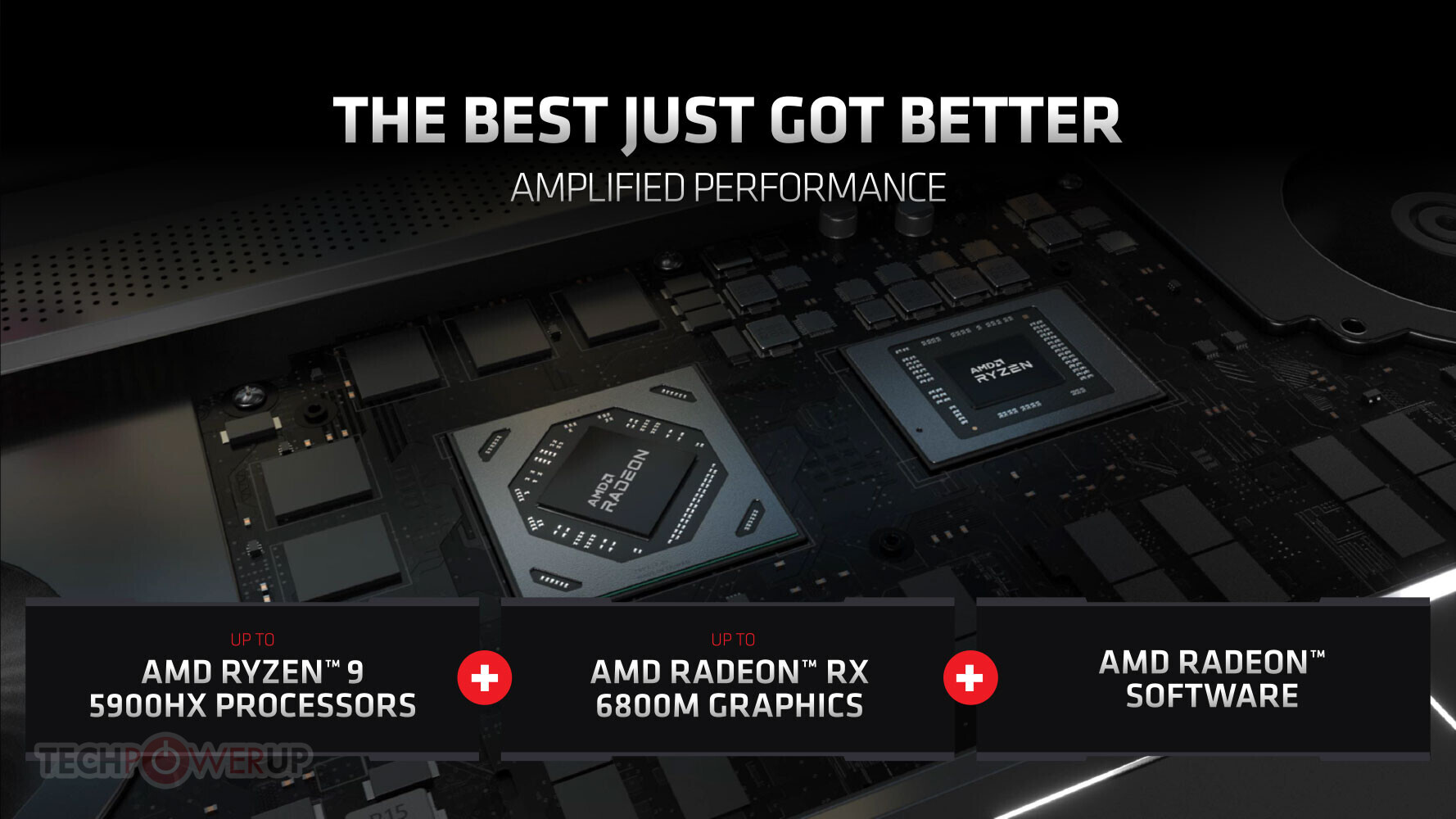
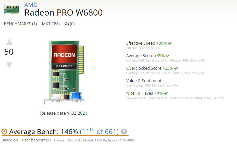
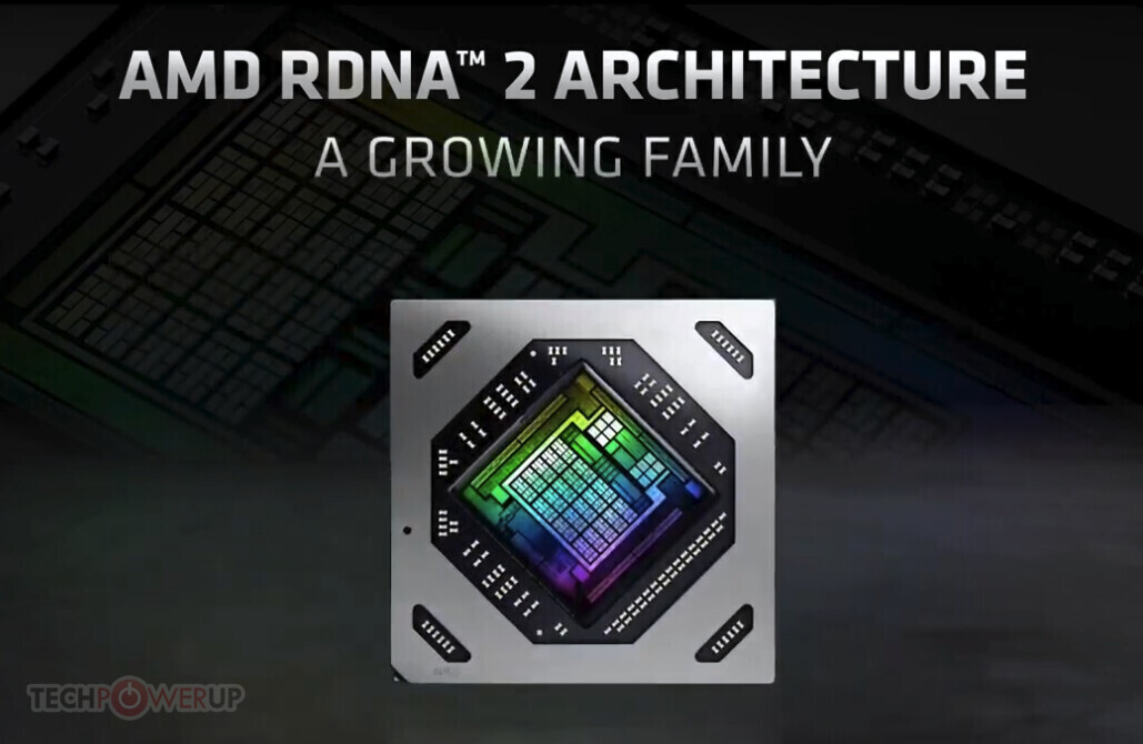
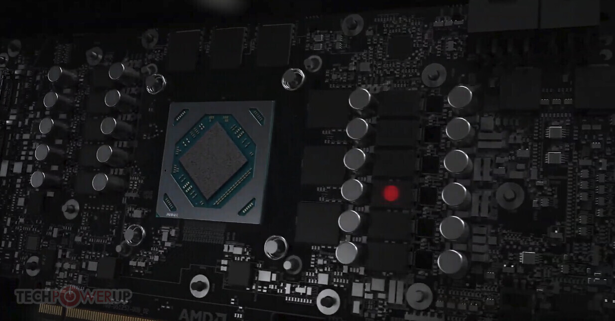
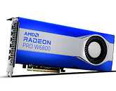
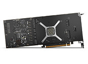
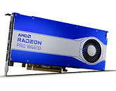
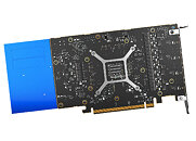
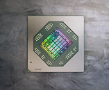
Built on award-winning AMD RDNA2 architecture, the foundation of next generation, high-powered PCs, laptops and many of today's game consoles, the new product line features the AMD Radeon PRO W6800, the fastest AMD RDNA workstation graphics card ever. It also includes the AMD Radeon PRO W6600 graphics card, meticulously engineered for ultra-high performance workflows, and the AMD Radeon PRO W6600M GPU, designed to power professional mobile workstations.

AMD Debuts Radeon RX 6000M Series Mobile Graphics Solutions

AMD today released the Radeon RX 6000M series mobile graphics lineup, based on the RDNA2 graphics architecture. These GPUs offer full DirectX 12 Ultimate readiness, including real-time raytracing capability. The lineup is led by the Radeon RX 6800M, followed by the RX 6700M, and the RX 6600M. The RX 6800M and RX 6700M are based on the 7 nm "Navi 22" silicon, while the RX 6600M debuts the "Navi 23" silicon. The RX 6800M appears to be maxing out the "Navi 22" silicon, much like the desktop RX 6700 XT. It features 40 RDNA2 compute units, amounting to 2,560 stream processors; game clocks of up to 2.30 GHz, 12 GB of GDDR6 memory across a 192-bit wide memory interface, and 96 MB of Infinity Cache. The RX 6700M is slightly cut down, with 36 compute units (2,304 stream processors), the same 2.30 GHz game clocks, 10 GB of video memory possibly across a 160-bit wide memory bus, and 80 MB of Infinity Cache.

The new RX 6600M debuts the 7 nm "Navi 23" silicon, with 28 RDNA2 compute units, game clocks of 2177 MHz, 8 GB of GDDR6 memory across a 128-bit wide memory bus, and 32 MB of Infinity Cache. All three chips feature Smart Access Memory (resizable BAR), and support for AMD SmartShift, a feature that load-balances the discrete GPU with an AMD iGPU. AMD claims that the RX 6800M and RX 6700M are fit for 1440p gaming, with the RX 6800M beating the RTX 2070 Notebook by anywhere between 40-70%, and 120 FPS in a large selection of e-sports titles. The company also claims that the RX 6800M beats the GeForce RTX 3080 8 GB by 14-39%. The RX 6600M, meanwhile is shown matching the RTX 3060 6 GB, in AMD's tests. Notebooks powered by AMD Radeon RX 6000M discrete graphics are shipping now.
The graphics press-deck follows.

Second TSMC Fab Worker Detected with COVID-19, Chip Shortages on the Anvil?

Taiwan's most valuable company, and chipmaker of the world, TSMC, confirmed that at least two of its fab workers have been diagnosed with COVID-19, but maintains that it doesn't affect operations at the plants. Most regions around world, including Taiwan, are bracing for successive waves of the disease, and a spread of COVID at TSMC could spell big trouble for the tech-giants dependent on the company for contract-manufacturing of their cutting-edge logic chips. Taiwan has been mostly spared from the Corona epidemic, but is now experiencing its largest wave of COVID-19 infections, with its medical infrastructure under strain. The latest outbreak has the potential to throw operations at TSMC off gear, affecting the supply chains of tens of billions of Dollars worth devices and vehicles around the world.

TSMC maintains an internal epidemic prevention committee, which has conducted contact-tracing of the the two employees, and discovered 10 contacts. Some of these have been sent to home-isolation, while others are closely monitoring themselves for symptoms. TSMC pledged that it will monitor the health of its employees on a daily basis. It has also completed the disinfection of the affected employees' workplace, and public areas visited by them. It once again emphasized that the incident will not affect company operations.

AMD Radeon "Navi 23" OEM Card, Possible RX 6600 XT Spied

A highly plausible looking AMD Radeon RX 6600 series graphics card is doing rounds on the web. The card is purportedly an AMD reference-design OEM-trim "Navi 23" board. We know from recent rumors that the 7 nm "Navi 23" silicon powers the upcoming Radeon RX 6600 XT and RX 6600. The picture only shows a portion of the card, the back-plate as viewed toward the rear I/O, but the bar-code sticker is unmistakable. The sticker reveals the OEM to be PC Partner, which is known to make all OEM and retail reference-design AMD Radeon graphics cards, which are marked "MBA" (made by AMD). You'll find a similar-looking bar-code sticker on all AMD reference-design cards, regardless of the AIB partner marketing it.

The bar-code sticker references "Navi 23 XT," which is very likely the Radeon RX 6600 XT. The card has 8 GB of GDDR6 memory, and its display outputs include one HDMI, and three DisplayPorts. Elsewhere in the picture, we get valuable insights into the design of the cooler, revealing that the card features an aluminium fin-stack heatsink with one or more axial fans (top-flow), rather than a channel-type lateral blower-type cooling solution. The "Navi 23" silicon is rumored to feature up to 32 RDNA2 compute units that amount to 2.048 stream processors, a PCI-Express 4.0 x8 host interface, much like the RX 5500 XT, and a 128-bit wide GDDR6 memory interface.

AMD and GlobalFoundries Wafer Supply Agreement Now Non-Exclusive, Paves Way for 7nm sIOD

AMD in a filing with the U.S. Securities and Exchange Commission (SEC), revealed that its wafer supply agreement with GlobalFoundries has been amended. Under the new terms, AMD places orders for wafers from GlobalFoundries up to 2024, with purchase targets set for each year leading up to 2024. Beyond meeting these targets, AMD is free from all other exclusivity commitments. The agreement was previously amended in January 2019, setting annual purchase targets for 2019, 2020, and 2021, while beginning a de-coupling between AMD and GlobalFoundries. This enabled the company to source 7 nm (or smaller) chips, such as CCDs and GPUs, from other foundries, such as TSMC, while keeping GlobalFoundries exclusive for 12 nm (or larger) nodes.

The updated wafer supply agreement unlocks many possibilities for AMD. For starters, it can finally build a next-generation sIOD (server I/O die) on a more efficient node than GlobalFoundries 12LP, such as TSMC 7 nm. This transition to 7 nm will be needed as the next-gen "Genoa" EPYC processor could feature future I/O standards such as DDR5 memory and PCI-Express Gen 5, and the switching fabric for these could be too power-hungry on 12 nm. The "Zen 4" CPU core complex dies (CCDs) of "Genoa" are expected to be built on TSMC 5 nm.

AMD "Navi 24" is the Smallest RDNA2 GPU Yet, Could Power RX 6400 Series

The 7 nm "Navi 24" silicon will very likely be the smallest discrete GPU based on the RDNA2 graphics architecture. The chip surfaced in technical documentation under the codename "Beige Goby." AMD uses such internal codenames to track sources of leaks. No specs of the "Navi 24" are known yet, but it could be significantly smaller than the "Navi 23" that powers the Radeon RX 6600 series and possibly the RX 6500 series, reportedly packing up to 2,048 stream processors. The "Navi 24" chip could also help AMD compete against NVIDIA and an emerging Intel in entry-level discrete GPUs for notebooks.

AMD Radeon Pro W6800 to Feature 32GB Memory

AMD's upcoming professional graphics card based on the 7 nm "Navi 21" silicon, the Radeon Pro W6800, will feature 32 GB of GDDR6 memory, according to a new leaked validation on the Userbenchmark database. The card was pictured and detailed in an older article that you can read here. It's likely that AMD achieved 32 GB over the chip's 256-bit wide memory bus using sixteen 16 Gbit memory chips, with two chips piggy-backed per 32-bit path. The picture leak from April also reveals a heatspreader over the reverse side of the otherwise bare PCB that points to the likelihood of memory chips being located there. On the client-segment Radeon RX 6800 XT, 16 GB is achieved using eight 16 Gbit chips, all of which are located on the obverse side. The exact specifications of the Pro W6800 remain unknown, but is expected to be comparable to the RX 6800 series.

Xilinx Reports Fiscal Fourth Quarter and Fiscal Year 2021 Results

Xilinx, Inc. (Nasdaq: XLNX), the leader in adaptive computing, today announced record revenues of $851 million for the fiscal fourth quarter, up 6% over the previous quarter and an increase of 13% year over year. Fiscal 2021 revenues were $3.15 billion, largely flat from the prior fiscal year. GAAP net income for the fiscal fourth quarter was $188 million, or $0.75 per diluted share. Non-GAAP net income for the quarter was $204 million, or $0.82 per diluted share. GAAP net income for fiscal year 2021 was $647 million, or $2.62 per diluted share. Non-GAAP net income for fiscal year 2021 was $762 million, or $3.08 per diluted share.

Additional fourth quarter of fiscal year 2021 comparisons are provided in the charts below. "We are pleased with our fourth quarter results as we delivered record revenues and double-digit year-over-year growth in the midst of a challenging supply chain environment," said Victor Peng, Xilinx president and CEO. "Xilinx saw further improvement in demand across a majority of our diversified end markets with key strength in our Wireless, Data Center and Automotive markets, the pillars of our growth strategy. Our teams have executed well and we remain focused on continuing to meet customers' critical needs.

Sony Reportedly Working on Redesigned PS5 SoC on 6 nm for 2022

It's not only graphics cards and CPUs that are best kept on the edge of manufacturing processes; in truth, one could even say that consoles have more to gain from these transitions when it comes to their manufacturers' financial outlooks. This happens because usually, consoles are subsidized by manufacturers in that their actual retail price is lower than manufacturing costs; this works as a way for console players to increase their platforms' attractiveness and user base, so they can then sell them games and subscription services, where the big bucks are actually made. We knew this already, but Microsoft's head of Xbox business development, Lori Wright confirmed it yesterday at the Apple vs Epic Games hearing. Lori Wright is quoted as answering "We don't; we sell the consoles at a loss" when asked whether Microsoft does or does not turn a profit on Xbox Series S | X hardware sales.

Considering the similarities between the Xbox Series X and PS5's SoC, it's very likely that Sony doesn't make a profit on console hardware sales either - or if it actually does, it's nothing actually meaningful. This is part of the reason why consoles are usually actually in the forefront of manufacturing processes' advancements, as it's a way for console players to quickly reduce the BoM (Bill of Materials) for their consoles. Since the specifications don't change within a console generation (discounting Pro models, which both companies have taken to launching some years into their generations), they choose to take advantage of process advancements due to the transistor density increases that allow for both lower silicon area for the SoC, and lower power consumption - which sometimes enables them to develop slim versions of their gaming consoles.

AMD Ryzen 7 5700G and Ryzen 5 5600G "Zen 3" Cezanne Desktop Processors Benched

Several benchmark numbers of the upcoming AMD Ryzen 7 5700G and Ryzen 5 5600G desktop processors were fished out by Thai PC enthusiast TUM_APISAK. The 5700G and 5600G are based on the 7 nm "Cezanne" silicon that combines up to 8 "Zen 3" CPU cores across a single CCX, sharing a single 16 MB L3 cache; along with an iGPU based on the "Vega" graphics architecture. Both chips were put through the CPU-Z Bench, where they posted spectacular results.

Both chips post higher single-thread score than the Core i9-10900K "Comet Lake," riding on the back of the high IPC of the "Zen 3" cores, and low latencies from the monolithic "Cezanne" silicon. In the multi-threaded test, the 8-core/16-thread 5700G scored above the Core i9-9900KS (5.00 GHz all-core). An HP OMEN 25L pre-built was put through Geekbench 5, where it was found performing within 90% of the Core i5-11600K. Userbenchmark remarks that the 5600X performs within the league of contemporaries, but falls behind on memory latency. Find the validation pages in the source links below.

PowerColor Teases Spectral White Color Trim of its RX 6700 XT Hellhound Graphics Card

PowerColor today teased an upcoming variant of its Radeon RX 6700 XT Hellhound graphics card, featuring an all-white PCB. It's likely that the card will be built around the white color-scheme, with white extending to the card's back-plate and cooler-shroud. It remains to be seen if any other changes are made to the RX 6700 XT Hellhound, such as clock-speeds, or lighting. Based on the 7 nm Navi 22 silicon, the RX 6700 XT features 2,560 stream processors, 40 Ray Accelerators, 144 TMUs, 64 ROPs, and a 192-bit wide memory interface, holding 12 GB of memory.

Cerebras Updates Wafer Scale Engine on 7 nm - 2.6 Trillion Transistors, 40 GB Onboard SRAM, 850,000 Cores, 12" Wafer

Cerebras has announced the successor to their record-breaking Wafer Scale Engine. The newly re-engineered Wafer Scale Engine 2 has been redesigned for TSMC's 7 nm manufacturing process - a severe improvement over the original's 16 nm. That Cerebras has moved on to TSMC's 7 nm for this giant, wafer-sized accelerator is telling of the confidence and state of yields on TSMC's 7 nm - if the process wasn't considered to be stable and guaranteeing incredibly good yields, I doubt such an effort would have been undertaken.

Tianshu Zhixin Big Island GPU is a 37 TeraFLOP FP32 Computing Monster

Tianshu Zhixin, a Chinese startup company dedicated to designing advanced processors for accelerating various kinds of tasks, has officially entered the production of its latest GPGPU design. Called "Big Island" GPU, it is the company's entry into the GPU market, currently dominated by AMD, NVIDIA, and soon Intel. So what is so special about Tianshu Zhixin's Big Island GPU, making it so important? Firstly, it represents China's attempt of independence from the outside processor suppliers, ensuring maximum security at all times. Secondly, it is an interesting feat to enter a market that is controlled by big players and attempt to grab a piece of that cake. To be successful, the GPU needs to represent a great design.

And great it is, at least on paper. The specifications list that Big Island is currently being manufactured on TSMC's 7 nm node using CoWoS packaging technology, enabling the die to feature over 24 billion transistors. When it comes to performance, the company claims that the GPU is capable of crunching 37 TeraFLOPs of single-precision FP32 data. At FP16/BF16 half-precision, the chip is capable of outputting 147 TeraFLOPs. When it comes to integer performance, it can achieve 317, 147, and 295 TOPS in INT32, INT16, and IN8 respectively. There is no data on double-precision floating-point numbers, so the chip is optimized for single-precision workloads. There is also 32 GB of HBM2 memory present, and it has 1.2 TB of bandwidth. If we compare the chip to the competing offers like NVIDIA A100 or AMD MI100, the new Big Island GPU outperforms both at single-precision FP32 compute tasks, for which it is designed.
Tianshu Zhixin Big Island Tianshu Zhixin Big Island Tianshu Zhixin Big Island Tianshu Zhixin Big Island
Pictures of possible solutions follow.

Intel Could Rename its Semiconductor Nodes to Catch Up with the Industry

In the past few years, Intel has struggled a lot with its semiconductor manufacturing. Starting from the 10 nm fiasco, the company delayed the new node for years and years, making it seem like it is never going to get delivered. The node was believed to be so advanced that it was unexpectedly hard to manufacture, giving the company more problems. Low yields have been present for a long time, and it is only recently that Intel has started shipping its 10 nm products. However, its competitor, TSMC, has been pumping out nodes at an amazing rate. At the time of writing, the Taiwanese giant is producing the 5 nm node, with a 4 nm node on the way.

So to remain competitive, Intel would need to apply a new tactic. The company has a 7 nm node in the works for 2023 when TSMC will switch to the 3 nm+ nodes. That represents a marketing problem, where the node naming convention is making Intel inferior to its competitors. To fix that, the company will likely start node renaming and give its nodes new names, that are corresponding to the industry naming conventions. We still have no information how will the new names look like, or if Intel will do it in the first place, so take this with a grain of salt.

Intel to Outsource a Part of 2023 Processor Production to TSMC

Intel's problems with processor production, especially with newer nodes like 10 nm and 7 nm, have been widely known. The company has not been able to deliver the latest semiconductor process on time and has thus delayed many product launches. However, things are looking to take a complete U-turn and the hell will freeze. During the "Intel Unleashed: Engineering the Future" webcast event that happened yesterday, the company made several announcements regarding the 7 nm process and its viability. We have already reported that the company is working on the new Meteor Lake processor lineup for 2023, supposed to be manufactured on the fixed 7 nm node.

However, it seems like Intel will have to tap external capacities to manufacture a part of its processor production. The company has confirmed that it will use an unknown TSMC process to manufacture a part of the 2023 processor lineup. That means that Intel and TSMC have already established the needed capacity and that TSMC has already booked wafer capacity for Intel. This has never happened before, as Intel always kept its processor production under the company roof. However, given that there is a huge demand for new semiconductor processes, Intel has to look at external manufacturing options to keep up with the demand.

Intel "Meteor Lake" a "Breakthrough Client Processor" Leveraging Foveros Packaging

Intel CEO Pat Gelsinger made the first official reference to the company's future-generation client processor, codenamed "Meteor Lake." Slated for market release in 2023, the processor's compute tile will be taped out in Q2-2021. Launching alongside the "Granite Rapids" enterprise processor, "Meteor Lake" will be a multi-chip module leveraging Intel's Foveros chip packaging technology.

Different components of the processor will be fabricated on different kinds of silicon fabrication nodes, and interconnected on the package using EMIB inter-die connections, or even silicon interposers. The compute tile is likely the tile containing the processor's CPU cores, and Intel confirmed a 7 nm-class foundry node for it. "Meteor Lake" will be a hybrid processor, much like the upcoming "Alder Lake," meaning that it will have two kinds of CPU cores, larger "high performance" cores that remain dormant when the machine is idling or dealing with lightweight workloads; and smaller "high efficiency" cores based on a low-power microarchitecture.

ASML Finishes Development of EUV Pellicles for Greater Sub-7nm Yields

ASML has finally finished development of EUV (Extreme Ultra Violet) pellicles to be employed in manufacturing processes that use the most energetic frequency of visible light to etch semiconductors onto wafers. Pellicles have been used for decades in the industry, and they are basically ultra-thin membranes that protect photomasks during the etching process - impeding particles from depositing in the substrate, which could lead to defects at the wafer level for every subsequent patterning that is laid on top of the impurity. Manufacturers such as TSMC have deployed EUV-powered manufacturing processes, but they have had to toil with potentially lower yields and increased costs with wafer analysis so as to reduce chances of defects appearing.

It's been a long time coming for EUV-capable pellicles, because these have different requirements compared to their traditional, non-EUV counterparts. However, once they are available on the market, it's expected that all semiconductor manufacturers with bleeding-edge manufacturing processes integrate them into their production flows. These will allow for better yields, which in turn should reduce overall pricing for the manufacturing processes. As an example, these EUV masks could be deployed on TSMC's 7 nm, 6 nm, 5 nm, and so on and so on. Other players other than ASML are also finishing their pellicle design, so the industry will have multiple options to integrate into their processes.

PowerColor Unveils Radeon RX 6700 XT Graphics Card

TUL Corporation, a leading and innovative manufacturer of AMD graphics cards since 1997, today announced the new PowerColor AMD Radeon RX 6700 XT graphics card. Powered by the groundbreaking AMD RDNA 2 gaming architecture and featuring AMD Infinity Cache, AMD Smart Access Memory and other advanced technologies, the new graphics card delivers the ultimate in 1440p gaming performance.

The PowerColor AMD Radeon RX 6700 XT graphics card is built upon 7 nm process technology and AMD RDNA 2 gaming architecture, designed to deliver the optimal combination of performance and power efficiency. AMD RDNA 2 based graphics cards are optimized to deliver real-time lighting, shadow and reflection realism with DirectX Raytracing (DXR). When paired with AMD FidelityFX, developers can combine rasterized and ray-traced effects to provide the ideal balance of image quality and gaming performance.

AMD Radeon RX 6700 XT: All You Need to Know

AMD today announced the Radeon RX 6700 XT, its fourth RX 6000 series graphics card based on the RDNA2 graphics architecture. The card debuts the new 7 nm "Navi 22" silicon, which is physically smaller than the "Navi 21" powering the RX 6800/RX 6900 series. The RX 6700 XT maxes out "Navi 22," featuring 40 RDNA2 compute units, amounting to 2,560 stream processors. These are run at a maximum Game Clock frequency of 2424 MHz, a significant clock speed uplift over the previous-gen. The card comes with 12 GB of GDDR6 memory across a 192-bit wide memory interface. The card uses 16 Gbps GDDR6 memory chips, so the memory bandwidth works out to 384 GB/s. The chip packs 96 MB of Infinity Cache on-die memory, which works to accelerate the memory sub-system. AMD is targeting a typical board power metric of 230 W. The power input configuration for the reference-design RX 6700 XT board is 8-pin + 6-pin.

AMD is marketing the RX 6700 XT as a predominantly 1440p gaming card, positioned a notch below the RX 6800. The company makes some staggering performance claims. Compared to the previous-generation the RX 6700 XT is shown beating the GeForce RTX 2080 Super. NVIDIA marketed the current-gen RTX 3060 Ti as having the same performance outlook. Things get interesting, where AMD shows that in select games, the RX 6700 XT can even beat the RTX 3070, a card NVIDIA marketed as matching its previous-gen flagship, the RTX 2080 Ti. AMD is pricing the Radeon RX 6700 XT at USD $479 (MSRP), which is very likely to be bovine defecation, given the prevailing market situation. The company announced a simultaneous launch of its reference-design and AIB custom-design boards, starting March 18, 2021.
AMD's performance claims follow.

Revenue of Top 10 Foundries Expected to Increase by 20% YoY in 1Q21 in Light of Fully Loaded Capacities, Says TrendForce

Demand in the global foundry market remains strong in 1Q21, according to TrendForce's latest investigations. As various end-products continue to generate high demand for chips, clients of foundries in turn stepped up their procurement activities, which subsequently led to a persistent shortage of production capacities across the foundry industry. TrendForce therefore expects foundries to continue posting strong financial performances in 1Q21, with a 20% YoY growth in the combined revenues of the top 10 foundries, while TSMC, Samsung, and UMC rank as the top three in terms of market share. However, the future reallocation of foundry capacities still remains to be seen, since the industry-wide effort to accelerate the production of automotive chips may indirectly impair the production and lead times of chips for consumer electronics and industrial applications.

TSMC has been maintaining a steady volume of wafer inputs at its 5 nm node, and these wafer inputs are projected to account for 20% of the company's revenue. On the other hand, owing to chip orders from AMD, Nvidia, Qualcomm, and MediaTek, demand for TSMC's 7 nm node is likewise strong and likely to account for 30% of TSMC's revenue, a slight increase from the previous quarter. On the whole, TSMC's revenue is expected to undergo a 25% increase YoY in 1Q21 and set a new high on the back of surging demand for 5G, HPC, and automotive applications.

AMD Radeon RX 6700 Series to Launch on March 18

AMD is expected to launch its Radeon RX 6700 XT performance-segment graphics card on March 18, 2021, according to French tech publication Cowcotland. This would put the launch over two weeks after NVIDIA's February 25 launch of the GeForce RTX 3060. The new RX 6700 series is expected to compete against the RTX 3060 series, and debuts the new 7 nm "Navi 22" silicon that's based on the RDNA2 architecture, and features 40 compute units (2,560 stream processors). The card comes with 12 GB of GDDR6 memory across a 192-bit wide memory bus, much like the RTX 3060. Cowcotland expects availability of the RX 6700 XT to be "very limited" at launch. Who knew?

Intel Xe HPC Multi-Chip Module Pictured

Intel SVP for architecture, graphics, and software, Raja Koduri, tweeted the first picture of the Xe HPC scalar compute processor multi-chip module, with its large IHS off. It reveals two large main logic dies built on the 7 nm silicon fabrication process from a third-party foundry. The Xe HPC processor will be targeted at supercomputing and AI-ML applications, so the main logic dies are expected to be large arrays of execution units, spread across what appear to be eight clusters, surrounded by ancillary components such as memory controllers and interconnect PHYs.

There appear to be two kinds of on-package memory on the Xe HPC. The first kind is HBM stacks (from either the HBM2E or HBM3 generation), serving as the main high-speed memory; while the other is a mystery for now. This could either be another class of DRAM, serving a serial processing component on the main logic die; or a non-volatile memory, such as 3D XPoint or NAND flash (likely the former), providing fast persistent storage close to the main logic dies. There appear to be four HBM-class stacks per logic die (so 4096-bit per die and 8192-bit per package), and one die of this secondary memory per logic die.

Intel Has Fixed its 7 nm Node, But Outsourcing is Still Going to Happen

Intel has today reported its Q4 2020 earnings disclosing full-year revenue with the current CEO Bob Swan, upcoming new CEO Pat Gelsinger, and Omar Ishrak, Chairman of Intel's board. During the call, company officials have talked about Intel's earnings and most importantly, addressing the current problems about the company's manufacturing part - semiconductor foundries. Incoming Intel CEO, Pat Gelsinger, has talked about the state of the 7 nm node, giving shareholders reassurance and a will to remain in such a position. He has made an argument that he has personally reviewed the progress of the "health and recovery of the 7 nm program."

The 7 nm node has been originally delayed by a full year amid the expectations, and as with the 10 nm node, we have believed that it is going to experience similar issues. However, the incoming CEO has reassured everyone that it is very much improving. The new 7 nm node is on track for 2023 delivery, when Intel is expected to compete with the 3 nm node of TSMC. Firstly, Intel will make a debut of the 7 nm node with client processors scheduled for 1H 2023 arrival, with data center models following that. The company leads have confirmed that Intel will stay true to its internal manufacturing, but have stressed that there will still be a need for some outsourcing to happen.

Chinese Tianshu Zhixin Announces Big Island GPGPU on 7 nm, 24 billion Transistors

Chinese company Shanghai Tianshu Zhixin Semiconductor Co., Ltd., commonly known (at least in Asia) as Tianshu Zhixin, has announced the availability of their special-purpose GPGPU, affectionately referred to as Big Island (BI). The BI chip is the first fully domestic-designed solution for the market it caters to, and features close to the latest in semiconductor manufacturing, being built on a 7 nm process featuring 2.5D CoWoS (chip-on-wafer-on-substrate) packaging. The chip is built towards AI and HPC applications foremost, with applications in other industries such as education, medicine, and security. The manufacturing and packaging processes seem eerily similar to those available from Taiwanese TSMC.

Tianshu Zhixin started work on the BI chip as early as 2018, and has announced that the chip features support for most AI and HPC data processing formats, including FP32, FP16, BF16, INT32, INT16, and INT8 (this list is not exhaustive). The company says the chip offers twice the performance of existing mainstream products on the market, and emphasizes its price/performance ratio. The huge chip (it packs as many as 24 billion transistors) is being teased by the company as offering as much as 147 TFLOPs in FP126 workloads, compared to 77.97 TFLOPs in the NVIDIA A100 (54 billion transistors) and 184.6 TFLOPS from the AMD Radeon Instinct MI100 (estimated at 50 billion transistors).

AMD "Cezanne" Confirmed to Quadruple Max Addressable L3 Cache Per Core Over "Renoir"

At her 2021 International CES keynote address, AMD CEO Dr. Lisa Su announced the Ryzen 5000 series mobile processor family, which the company thinks has what it takes to beat Intel's 11th Gen Core "Tiger Lake" processor, possibly even its upcoming 8-core version. The Ryzen 5000 mobile processor is based on the new 7 nm "Cezanne" monolithic SoC die. This chip features an 8-core CPU based on the latest "Zen 3" microarchitecture, and its biggest change is the advent of the 8-core CCX, which means all eight cores on "Cezanne" share a common L3 cache.

AMD slides from the CES keynote confirm that the company has not only doubled the L3 cache amount compared to "Renoir," but also quadrupled the maximum addressable L3 cache per core. On "Renoir," the eight cores are split between two CCXs, each with 4 MB of L3 cache. "Cezanne" features a single 8-core CCX with 16 MB of it. The dedicated L2 cache amount remains at 512 KB per core. The "total cache" (L2+L3) adds up to 20 MB. For the 45-Watt Ryzen 5000 HX-series enthusiast mobile processors, the increased caches, coupled with improved IPC and higher clock speeds should be AMD's play against Intel's top H-segment mobile chips. AMD claims that the second-fastest Ryzen 9 5900HX beating Intel's fastest Core i9-10980HK by 13% in raw single-thread performance, 19% in game physics performance, and 35% in overall PassMark performance. The 5980HX should only end up faster.
Return to Keyword Browsing
Apr 26th, 2024 01:32 EDT change timezone

New Forum Posts

Popular Reviews

Controversial News Posts