News Posts matching #7 nm

Return to Keyword Browsing

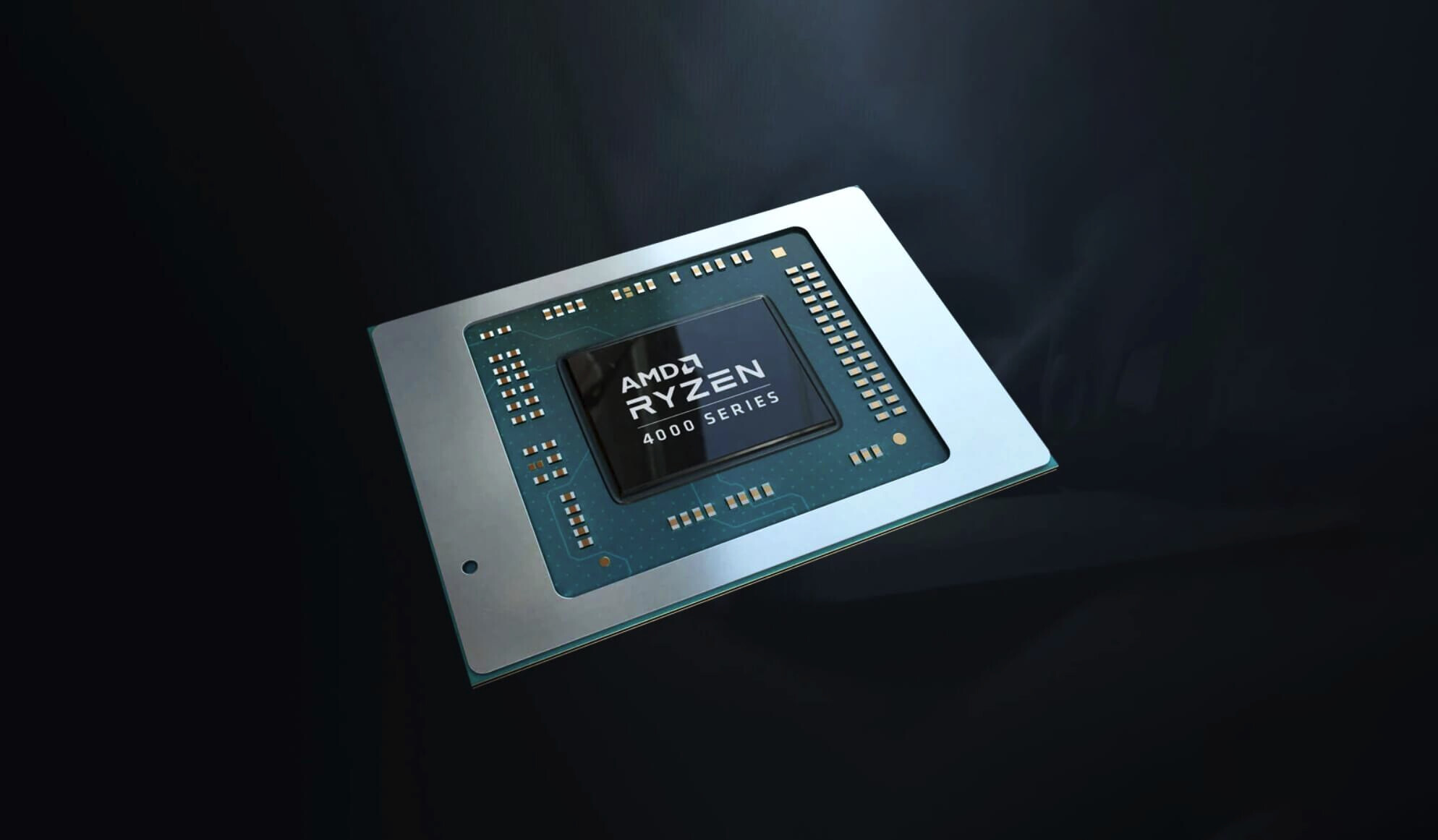
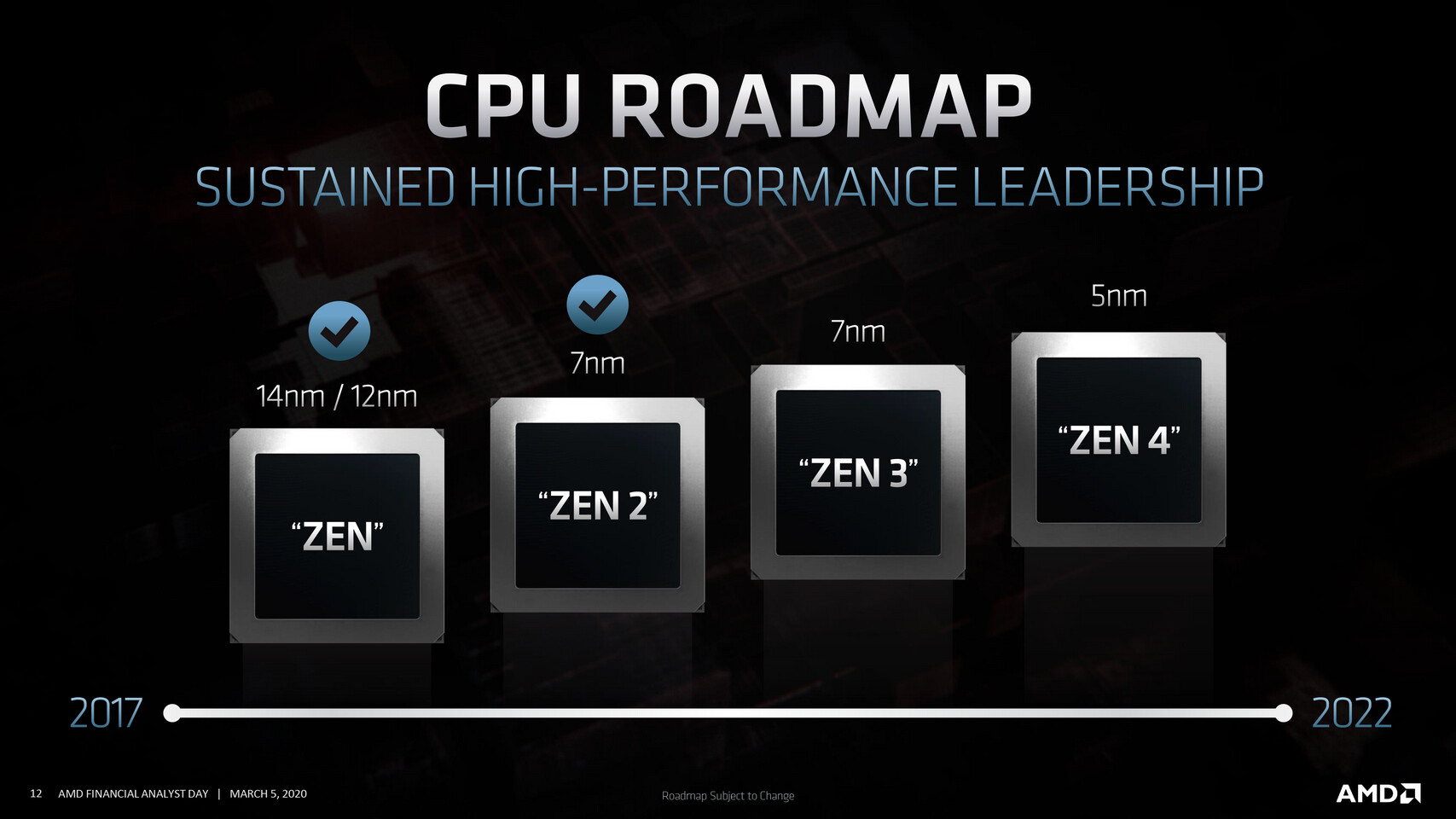
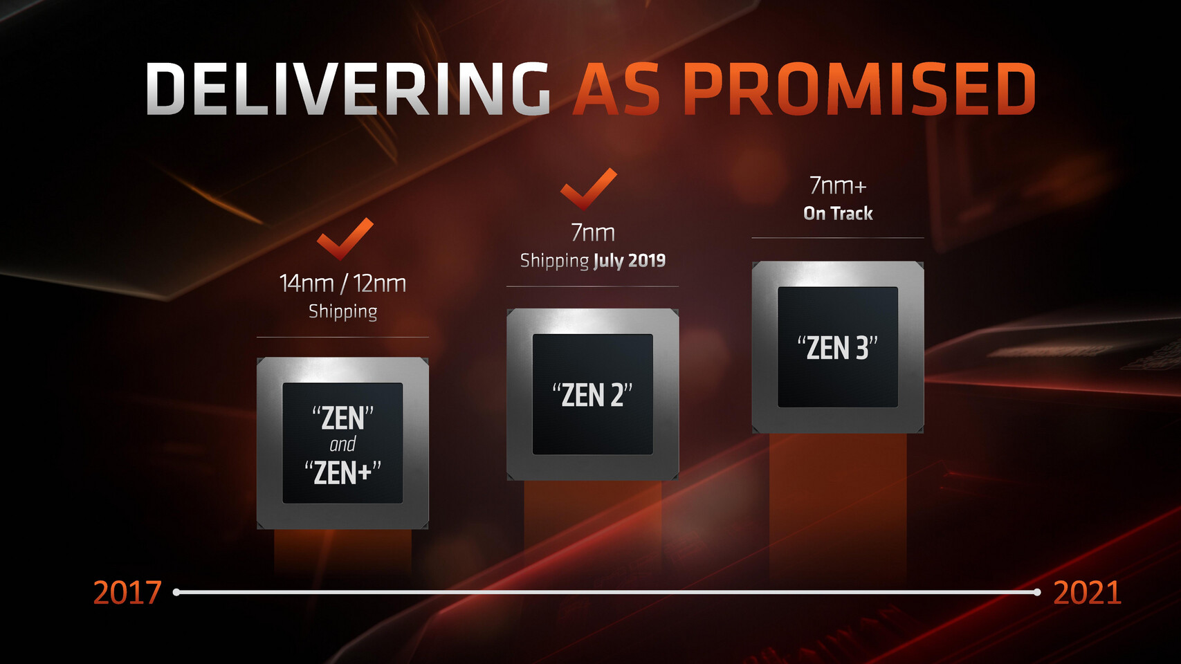
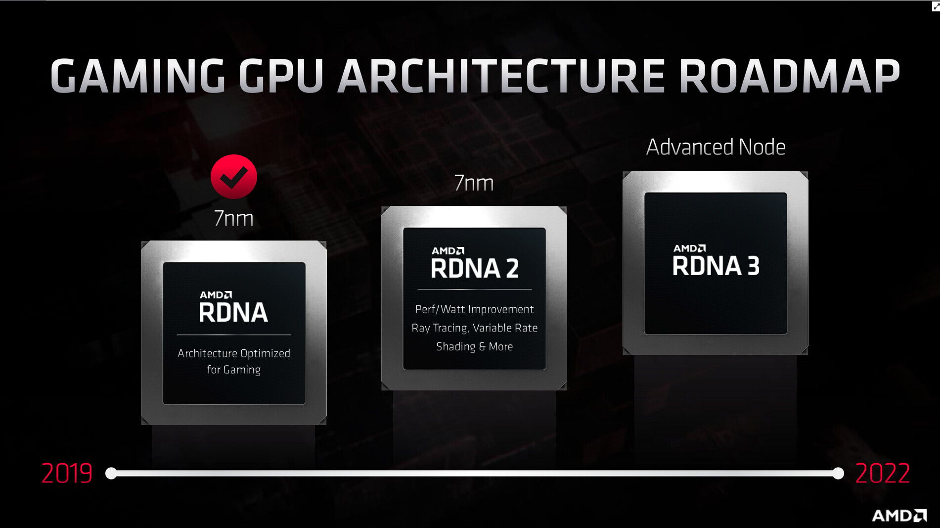
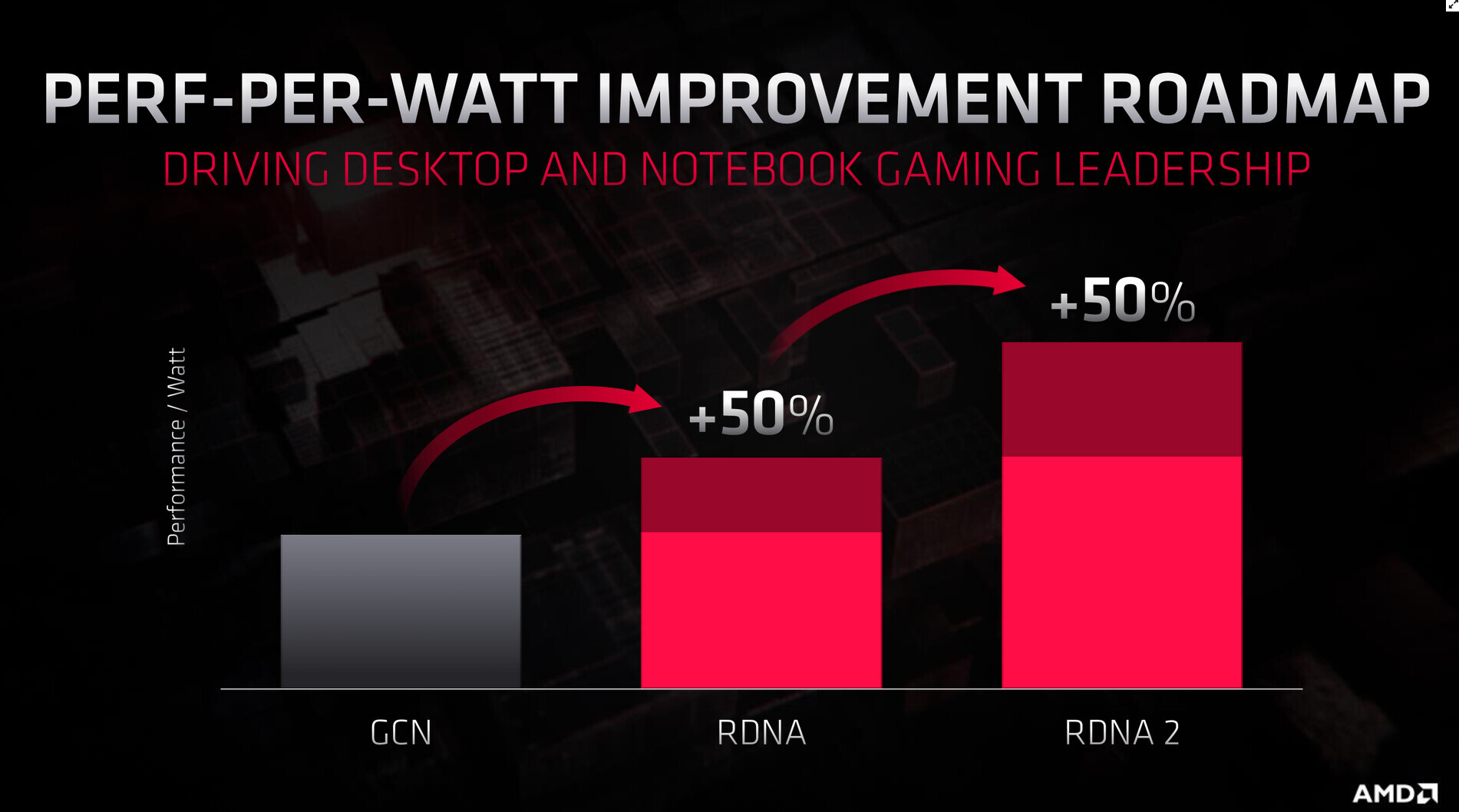
AMD "Renoir" Successor is "Cézanne," Powered by "Zen 3" and RDNA2

AMD's 7 nm "Renoir" silicon breathed life into the notebook processor market, by bringing 8-core/16-thread CPU performance into segments Intel reserved for 4-core/8-thread; and beat Intel in the iGPU performance front. 7 nm brought performance-Watt uplifts that spell serious competition for Intel across all notebook form factors, be it 15 W or 45 W. According to _rogame, who has a knack of getting far-out hardware rumors right, AMD has its successor on the drawing-board, and it's codenamed "Cézanne," after the French post-impressionist painter Paul Cézanne.

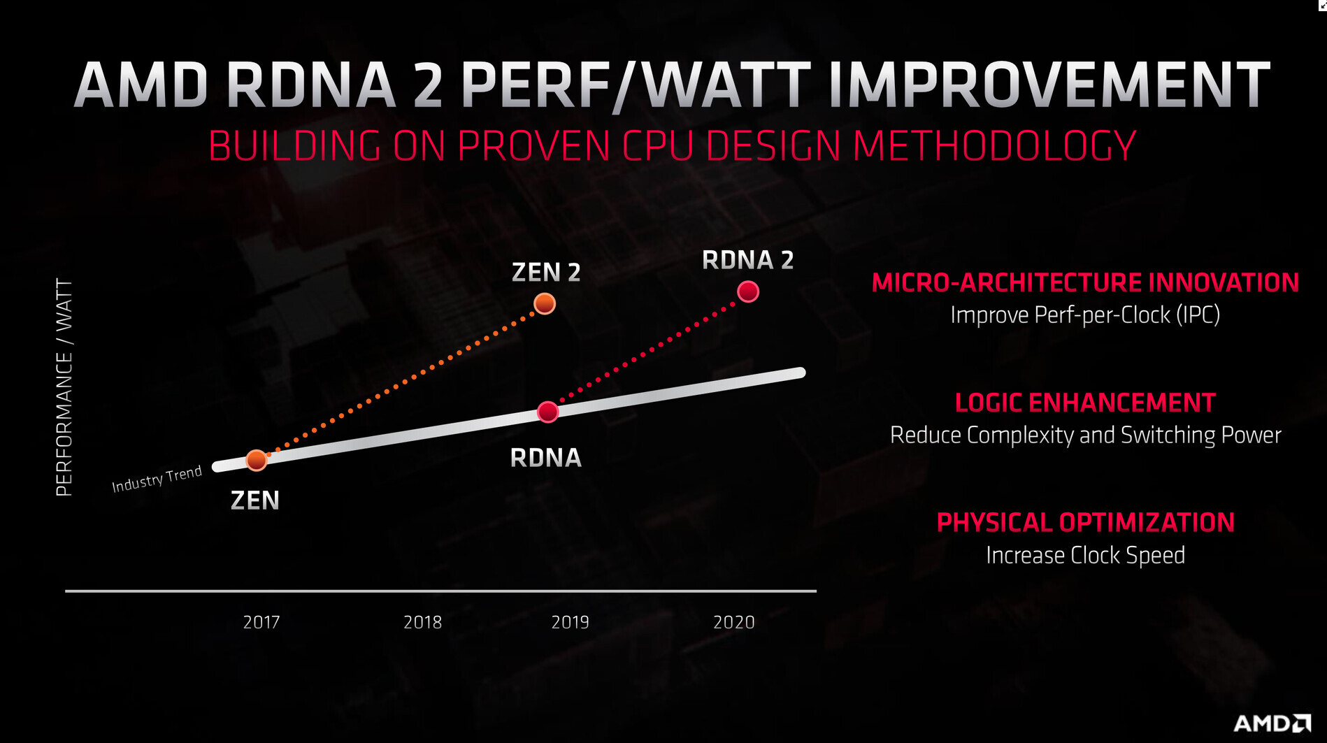
"Cézanne" could prove vital for AMD's foothold in the premium mobile computing segments as Intel is preparing to launch its 10 nm+ "Tiger Lake" processor soon, with advanced "Willow Cove" CPU cores, and Xe based integrated graphics. AMD plans to tap into its very latest IP. Although its core-count is not known, "Cézanne" will feature CPU cores based on the latest "Zen 3" microarchitecture. The iGPU will receive its biggest performance uplift in 3 generations, with an iGPU based on the cutting-edge RDNA2 graphics architecture that meets DirectX 12 Ultimate logo requirements.

NVIDIA is Secretly Working on a 5 nm Chip

According to the report of DigiTimes, which talked about TSMC's 5 nm silicon manufacturing node, they have reported that NVIDIA is also going to be a customer for it and they could use it in the near future. And that is very interesting information, knowing that these chips will not go in the next generation of GPUs. Why is that? Because we know that NVIDIA will utilize both TSMC and Samsung for their 7 nm manufacturing nodes for its next-generation Ampere GPUs that will end up in designs like GeForce RTX 3070 and RTX 3080 graphics cards. These designs are not what NVIDIA needs 5 nm for.

Being that NVIDIA already has a product in its pipeline that will satisfy the demand for the high-performance graphics market, maybe they are planning something that will end up being a surprise to everyone. No one knows what it is, however, the speculation (which you should take with a huge grain of salt) would be that NVIDIA is updating its Tegra SoC with the latest node. That Tegra SoC could be used in a range of mobile devices, like the Nintendo Switch, so could NVIDIA be preparing a new chip for Nintendo Switch 2?
NVIDIA Xavier SoC

AMD 35W "Artic" APU with High Nominal Clock Hints at "Renoir" Desktop Version

While AMD's 7 nm "Renoir" APU silicon is off busy disrupting the mobile processor market, AMD needs a socket AM4 desktop APU to challenge Intel's Core i5 and Core i7 chips that have iGPUs, and it's only natural for "Renoir" to reach the desktop platform at some point. PC enthusiast _rogame unearthed details of a 35-Watt TDP AMD APU codenamed "Artic," with a rather high 3.00 GHz nominal clock speed, which could hint at the possibility of this being a desktop part. The part in question also features an iGPU ticking at 1200 MHz, and DDR4-3200 memory.

AMD has released Renoir on the mobile platform at 15 W and 45 W power-envelopes. It has, in the past, similarly segmented its desktop APUs into 65 W and energy-efficient 35 W TDP parts, with the latter using lower clock speeds and aggressive power-management to hold on to its TDP. This chip could be the latter, a possible "Ryzen 3 4200GE" of sorts. _rogame mentions that the iGPU performance is a notch lower than the 6 CU "Renoir" parts such as the 4600H, while the CPU performance is higher than the 8-core/8-thread 4700U. Here's hoping we find out more soon.

Intel Gen12 Xe iGPU Could Match AMD's Vega-based iGPUs

Intel's first integrated graphics solution based on its ambitious new Xe graphics architecture, could match AMD's "Vega" architecture based iGPU solutions, such as the one found in its latest Ryzen 4000 series "Renoir" iGPUs, according to leaked 3DMark FireStrike numbers put out by @_rogame. Benchmark results of a prototype laptop based on Intel's "Tiger Lake-U" processor surfaced on the 3DMark database. This processor embeds Intel's Gen12 Xe iGPU solution, which is purported to offer significant performance gains over current Gen11 and Gen9.5 based iGPUs.

The prototype 2-core/4-thread "Tiger Lake-U" processor with Gen12 graphics yields a 3DMark FireStrike score of 2,196 points, with a graphics score of 2,467, and 6,488 points physics score. These scores are comparable to 8 CU Radeon Vega iGPU solutions. "Renoir" tops out at 8 CUs, but shores up performance to the 11 CU "Picasso" levels by other means. Besides tapping into the 7 nm process to increase engine clocks, improve the boosting algorithm, and modernizing the display- and multimedia engines; AMD's iGPU is largely based on the same 3-year old "Vega" architecture. Intel Gen12 Xe makes its debut with the "Tiger Lake" microarchitecture slated for 2021.

Apple's A12Z SoC Features the Same A12X Silicon

With an introduction of new iPad Pro tablets, Apple has brought another new silicon to its offerings in the form of A12Z SoC. Following the previous king in tablet space, the A12X SoC, Apple has decided to update its silicon and now there is another, more advanced stepping in form of an A12Z SoC. Thanks to the report from TechInsights, their analysis has shown that the new SoC used in Apple's devices is pretty much the same compared to the A12X SoC of last year, except the GPU used. Namely, the configuration of A12X is translated into the A12Z - there are four Apple Vortex and four Apple Tempest cores for the CPU. There is a 128-bit memory bus designed for LPDDR4X memory, the same as the A12X.

What is different, however, is the GPU cluster configuration. In A12X there was a cluster filled with 7 working and one disabled A12-gen GPU core. In A12Z SoC all of the 8 GPUs present are enabled and working, and they are also of the same A12 generation. The new SoC is even built using the same N7 7 nm manufacturing process from TSMC. While we don't know the silicon stepping revision of the A12Z, there aren't any new features besides the additional GPU core.
Apple A12Z Bionic

Huawei Moves 14 nm Silicon Orders from TSMC to SMIC

Huawei's subsidiary, HiSilicon, which designs the processors used in Huawei's smartphones and telecommunications equipment, has reportedly moved its silicon orders from Taiwan Semiconductor Manufacturing Company (TSMC) to Semiconductor Manufacturing International Corporation (SMIC), according to DigiTimes. Why Huawei decided to do is move all of the 14 nm orders from Taiwanese foundry to China's largest silicon manufacturing fab, is to give itself peace of mind if the plan of the US Government goes through to stop TSMC from supplying Huawei. At least for the mid-tier chips built using 14 nm node, Huawei would gain some peace as a Chinese fab is a safer choice given the current political situation.

When it comes to the high-end SoCs built on 7 nm, and 5 nm in the future, it is is still uncertain how will Huawei behave in this situation, meaning that if US cuts off TSMC's supply to Huawei, they will be forced to use SMIC's 7 nm-class N+1 node instead of anything from TSMC. Another option would be Samsung, but it is a question will Huawei put itself in risk to be dependant on another foreign company. The lack of 14 nm orders from Huawei will not be reflecting much on TSMC, because whenever someone decides to cut orders, another company takes up the manufacturing capactiy. For example, when Huawei cut its 5 nm orders, Apple absorbed by ordering more capacity. When Huawei also cut 7 nm orders, AMD and other big customers decided to order more, making the situation feel like there is a real fight for TSMC's capacity.
Silicon Wafer

Samsung to Deliver 3 nm Manufacturing Process in 2022 with Next-Generation Transistors

Samsung is determined in its plans to deliver the 3 nm silicon manufacturing process in the year 2022, and with it, there will be some major improvements to the transistor technology. We have already mentioned that Samsung is working on Gate-All-Around FET technology that will bring much better control of the transistor channel, preventing leakage at smaller nodes. However, today Samsung added a few more details about its upcoming Multi Bridge Channel FET technology for a 3 nm manufacturing process, simply called the MBCFET. Thanks to the report from Hardwareluxx, we have more details regarding the MBCFET technology and its characteristics.

Firstly, it is worth noting that MCBFET is a part of GAAFETs, meaning that the GAAFET is not one product, but rather a class of many based on its concepts. As far as the MCBFET performance goes, Samsung says that the technology will use 50% less power while delivering 30% more performance. There is going to be a big density gain as well, where Samsung predicts there will be around 45% less silicon space taken per one transistor. The comparison is made to an unspecified 7 nm process, possibly Samsung's process that uses FinFETs. The technology allows the stacking of transistors on top of each other, which makes it use inherently less space compared to regular FinFET. Being that MCBFET GAA transistors make its transistor width flexible, it means that the overall stacked transistor can be as wide as a designer needs it to be, adjusting for any scenario like low-power or high-performance.
Samsung GAA Samsung MBCFET

AMD 4th Gen Ryzen Desktop Processors to Launch Around September 2020

AMD's 4th generation Ryzen desktop processors are expected to launch around September 2020, sources in the motherboard industry tell DigiTimes. Codenamed "Vermeer," successor to "Matisse," these processors will be socket AM4 multi-chip modules of up to two CPU complex dies based on the "Zen 3" microarchitecture, combined with an I/O controller die. The "Zen 3" chiplets are expected to be fabricated on a newer 7 nm-class process by TSMC, either N7P or N7+. The biggest design change with "Zen 3" is the doing away of CCX arrangement of CPU cores, with each chiplet holding a common block of cores sharing a last-level cache. This, along with clock speed headroom gains from the new node are expected to yield generational price-performance increases.

The "Zen 2" based 8-core "Renoir" die is also expected to make its socket AM4 debut within 2020, succeeding the "Picasso" based quad-core Ryzen 3000-series APUs. This is a particularly important product for AMD, as it is expected to compete with Intel's 10th generation Core i5 6-core/12-thread processors in terms of pricing, while offering more cores (8-core/16-thread) and a faster iGPU. The 4th gen Ryzen socket AM4 processor lineup will launch alongside AMD's 600-series motherboard chipset, with forwards- and backwards-compatibility (i.e., "Vermeer" and "Renoir" working with older chipsets, and older AM4 processors working on 600-series chipset motherboards). AMD was originally expected to unveil these processors at the 2020 Computex trade-show in June, but Computex itself is rescheduled to late-September.

SMIC 7nm-class N+1 Foundry Node Going Live by Q4-2020

China's state-backed SMIC (Semiconductor Manufacturing International Corporation) has set an ambitious target of Q4-2020 for its 7 nanometer-class N+1 foundry node to go live, achieving "small scale production," according to a cnTechPost report. The company has a lot of weight on its shoulders as geopolitical hostility between the U.S. and China threatens to derail the country's plans to dominate 5G technology markets around the world. The SMIC N+1 node is designed to improve performance by 20%, reduce chip power consumption by 57%, reduce logic area by 63%, and reduce SoC area by 55%, in comparison to the SMIC's 14 nm FinFET node, Chinese press reports citing a statement from SMIC's co-CEO Dr. Liang Mengsong.

Dr. Liang confirmed that the N+1 7 nm node and its immediate successor will not use EUV lithography. N+1 will receive a refinement in the form of N+2, with modest chip power consumption improvement goals compared to N+1. This is similar to SMIC's 12 nm FinFET node being a refinement of its 14 nm FinFET node. Later down its lifecycle, once the company has got a handle of its EUV lithography equipment, N+2 could receive various photomasks, including a switch to EUV at scale.

DDR5 Arrives at 4800 MT/s Speeds, First SoCs this Year

Cadence, a fabless semiconductor company focusing on the development of IP solutions and IC design and verification tools, today posted an update regarding their development efforts for the 5th generation of DDR memory which is giving us some insights into the development of a new standard. The new DDR5 standard is supposed to bring better speeds and lower voltages while being more power-efficient. In the Cadence's blog called Breakfast Bytes, one of Cadence's memory experts talked about developments of the new standards and how they are developing the IP for the upcoming SoC solutions. Even though JEDEC, a company developing memory standards, hasn't officially published DDR5 standard specifications, Cadence is working closely with them to ensure that they stay on track and be the first on the market to deliver IP for the new standard.

Marc Greenberg, a Cadence expert for memory solutions was sharing his thoughts in the blog about the DDR5 and how it is progressing. Firstly, he notes that DDR5 is going to feature 4800 MT/s speeds at first. The initial speeds will improve throughout the 12 months when the data transfer rate will increase in the same fashion we have seen with previous generation DDR standards. Mr. Greenberg also shared that the goals of DDR5 are to have larger memory dies while managing latency challenges, same speed DRAM core as DDR4 with a higher speed I/O. He also noted that the goal of the new standard is not the bandwidth, but rather capacity - there should be 24Gb of memory per die initially, while later it should go up to 32Gb. That will allow for 256 GB DIMMs, where each byte can be accessed under 100 ns, making for a very responsive system. Mr. Greenberg also added that this is the year of DDR5, as Cadence is receiving a lot of orders for their 7 nm IP which should go in production systems this year.
Cadence DDR5

U.S. Government Tightens Screws on Huawei's Global Chip Supply from TSMC

The U.S. government announced advanced measures that make it harder for foreign companies, such as Taiwan's TSMC, to supply chips to Chinese telecom hardware giant Huawei. Foreign companies that use American chipmaking equipment, are required to obtain a license from the U.S. before supplying certain chips to Huawei. Sources comment that the new rule was tailor-made to curb TSMC fabricating smartphone SoCs for Huawei's HiSilicon subsidiary.

Mainland Chinese semiconductor companies are still behind Samsung and TSMC in 7 nm-class fab technologies, forcing HiSilicon to source from the latter. 7 nm fabrication is a key requirement for SoCs and modem chips capable of 5G. The high data transceiving rates of 5G requires a certain amount of compute power that can fit into smartphone-level power-envelopes only with the help of 7 nm, at least for premium smartphone form-factors. Same applies to 5G infrastructure equipment. This is hence perceived as a means for the U.S. to clamp brakes on Huawei's plans of playing a big role in 5G tech rollouts around the world, buying western 5G tech suppliers such as Nokia time to catch up. Huawei has been a flashpoint for a bitter political spat between the U.S. and China, with the Chinese press even threatening that the matter could hamper medical supplies to the U.S. to fight the COVID-19 pandemic.

TSMC N5P 5nm Node Offers 84-87% Transistor Density Gain Over Current 7nm Node

A WikiChip analysis of TSMC's next-generation 5 nanometer N5P silicon fabrication node estimates a massive 84-87% increase in transistor densities on offer compared to the company's first commercial 7 nm-class node, the N7 (7 nm DUV). The report estimates an 87% transistor-density increase, even though TSMC's own figure is slightly modest, at 84%. TSMC N5P node is expected to commence production later this year. Its precursor, TSMC N5, began risk production earlier this year, with production on the node commencing in April or May, unless derailed by the COVID-19 pandemic. The N5P node provides transistor densities of an estimated 171.3 million transistors per mm² die area, compared to 91.2 mTr/mm² of N7. Apple is expected to be the node's biggest customer in 2020, with the company building its A14-series SoC on it.

Sony Reveals PS5 Hardware: RDNA2 Raytracing, 16 GB GDDR6, 6 GB/s SSD, 2304 GPU Cores

Sony in a YouTube stream keynote by PlayStation 5 lead system architect Mark Cerny, detailed the upcoming entertainment system's hardware. There are three key areas where the company has invested heavily in driving forward the platform by "balancing revolutionary and evolutionary" technologies. A key design focus with PlayStation 5 is storage. Cerny elaborated on how past generations of the PlayStation guided game developers' art direction as the low bandwidths and latencies of optical discs and HDDs posed crippling latencies arising out of mechanical seeks, resulting in infinitesimally lower data transfer rates than what the media is capable of in best case scenario (seeking a block of data from its outermost sectors). SSD was the #1 most requested hardware feature by game developers during the development of PS5, and Sony responded with something special.

Each PlayStation 5 ships with a PCI-Express 4.0 x4 SSD with a flash controller that has been designed in-house by Sony. The controller features 12 flash channels, and is capable of at least 5.5 GB/s transfer speeds. When you factor in the exponential gains in access time, Sony expects the SSD to provide a 100x boost in effective storage sub-system performance, resulting in practically no load times.

AMD "Renoir" Die Shot Pictured

Here is the first die visualization of AMD's new "Renoir" processor. Having made its debut with Ryzen 4000 series mobile processors, "Renoir" succeeds a decade-long legacy of AMD APUs that combine CPUs with powerful iGPUs. AMD designed "Renoir" on TSMC's 7 nm silicon fabrication process. The die measures 156 mm², and has a transistor-count of 9.8 billion. The die shot reveals distinct areas that look like the processor's 8 CPU cores, a cluster of GPU compute units, the integrated memory controllers, southbridge, and PHYs for the chip's various I/O.

"Renoir" features 8 CPU cores based on the "Zen 2" microarchitecture, divided into two 4-core CCXs (CPU complexes). Unlike on 8-core chiplets meant for "Matisse" or "Rome" MCMs, the "Renoir" CCX only features 4 MB of shared L3 cache, probably because latencies to the memory controller are low enough. The L2 cache per core is unchanged at 512 KB. The "total cache" (L2 + L3 on silicon) adds up to 12 MB. The iGPU of "Renoir" is a hybrid between "Vega" and "Navi." The SIMD components are carried over from "Vega," while the display- and multimedia engines are from "Navi." The iGPU features 8 NGCUs that add up to 512 stream processors. Infinity Fabric covers much of the die area, connecting the various components on the die. AMD introduced a new dual-channel integrated memory controller that supports LPDDR4x at up to 4233 MHz, and standard DDR4 up to 3200 MHz.
AMD Renoir die AMD Renoir die annotation

Complete Hardware Specs Sheet of Xbox Series X Revealed

Microsoft just put out of the complete hardware specs-sheet of its next-generation Xbox Series X entertainment system. The list of hardware can go toe to toe with any modern gaming desktop, and even at its production scale, we're not sure if Microsoft can break-even at around $500, possibly counting on game and DLC sales to recover some of the costs and turn a profit. To begin with the semi-custom SoC at the heart of the beast, Microsoft partnered with AMD to deploy its current-generation "Zen 2" x86-64 CPU cores. Microsoft confirmed that the SoC will be built on the 7 nm "enhanced" process (very likely TSMC N7P). Its die-size is 360.45 mm².

The chip packs 8 "Zen 2" cores, with SMT enabling 16 logical processors, a humongous step up from the 8-core "Jaguar enhanced" CPU driving the Xbox One X. CPU clock speeds are somewhat vague. It points to 3.80 GHz nominal and 3.66 GHz with SMT enabled. Perhaps the console can toggle SMT somehow (possibly depending on whether a game requests it). There's no word on the CPU's cache sizes.

Xbox Series X Semi-custom SoC Features 320-bit Memory Interface, 10 GB or 20 GB Memory

Microsoft's upcoming Xbox Series X entertainment system is shaping up to be a technological monstrosity. Xbox group head at Microsoft, Phil Spencer, last revealed a picture of its semi-custom SoC back in January, by setting it as his Twitter display picture. Over the following weeks, many more technical details, such as the chip's 12 TFLOP/s combined compute power, would be let out. Spencer updated his display picture revealing a segment of the Xbox Series X mainboard with the SoC and memory chips surrounding it. The picture reveals the large SoC package in the center, surrounded on three sides by ten memory chips, possibly GDDR6, each with its own wiring to the SoC. This indicates that the SoC features a 320-bit wide memory interface.

As for the memory density, there's no way to tell. It could be 10 GB if those are 8 Gbit memory chips, or 20 GB if those are 16 Gbit. It boils down to which device the Xbox Series X the company wants to succeed. The Xbox One S features 8 GB of DDR3, while the spruced up Xbox One X features 12 GB of GDDR5. If the new Xbox Series X succeeds the latter, then it could very well feature 20 GB, more so given Microsoft's lofty design goals (4K UHD gaming with real-time ray-tracing). Microsoft leverages hUMA to use a common memory pool for both the CPU and GPU. Designed in collaboration with AMD on a TSMC 7 nm-class node (likely the N7P), the SoC features "Zen 2" CPU cores, and a GPU based on the RDNA2 graphics architecture.
Xbox Series X memory

TechPowerUp GPU-Z 2.30.0 Released

TechPowerUp today released the latest version of GPU-Z, the popular graphics subsystem information and diagnostic utility. Version 2.30.0 introduces several new feature- and stability updates, and adds support for new GPUs. To begin with, support is added for AMD Radeon RX 590 GME, Radeon Pro W5500, Pro V7350x2, FirePro 2260, and Instinct MI25 MxGPU; Intel UHD (Core i5-10210Y), and a rare GeForce GTS 450 Rev 2. TechPowerUp GPU-Z 2.30.0 introduces support for reporting hardware-accelerated GPU scheduling in Windows 10 20H1 in the Advanced tab. The tab now also has the ability to show WDDM 2.7, Shader Model 6.6, DirectX Mesh Shaders, and DXR tier 1.1. A workaround for the DirectML detection on Windows 10 19041 built has been added. Graphics driver registry path is now displayed in the General section of the Advanced tab.

In the Sensors tab, the NVIDIA VDDC sensor has been renamed to "GPU voltage," and AMD's "GPU only power draw" sensor to "GPU chip-only power draw" to clarify that the sensor only measures the power draw of the GPU package and not the whole graphics card. AMD "Renoir" based processors and their iGPUs now show up as 7 nm. Windows Basic Display driver now no longer reports its status as WHQL or Beta. A crash during DirectX 12 detection has been fixed.
TechPowerUp GPU-Z 2.23.0 main window
DOWNLOAD: TechPowerUp GPU-Z 2.30.0

The change-log follows.

AMD Sheds Light on the Missing "+" in "7nm" for Zen 3 and RDNA2 in its Latest Presentation

AMD at its Financial Analyst Day 2020 presentation made a major clarification about its silicon fabrication process. It was previously believed that the company's upcoming "Zen 3" CPU microarchitecture and RDNA2 graphics architectures were based on TSMC's N7+ (7 nm EUV) silicon fabrication process because AMD would mark the two as "7 nm+" in its marketing slides. Throughout its Financial Analyst Day presentation, however, AMD avoided using that marker, and resorted to an amorphous "7 nm" marker, prompting one of the financial analysts to seek a clarification. At the time, AMD responded that they were aligning their marketing with that of TSMC, and hence chose to use "7 nm" in its new slides.

It turns out that the next step to TSMC N7, the company's current-generation 7 nm DUV silicon fabrication node, isn't N7+ (7 nm EUV), but rather it has a nodelet along the way, which the foundry refers to as N7P. This is a generational refinement of N7, but does not use EUV lithography, which means it may not offer the 15-20 percent gains in transistor densities offered by N7+ over N7. AMD clarified that "7 nm+" in its past presentations did not intend to signify N7+, and that the "+" merely denoted an improvement over N7. At the same time, it won't specify whether "Zen 3" and RDNA2 are based on N7P or N7+, so the company doesn't rule out N7+, either. We'll probably learn more as we near the late-2020 launch of "Zen 3" as EPYC "Milan."
AMD CPU Roadmap Zen 3 Zen 4 AMD CPU Roadmap Zen 2 Zen 3

AMD RDNA2 Graphics Architecture Detailed, Offers +50% Perf-per-Watt over RDNA

With its 7 nm RDNA architecture that debuted in July 2019, AMD achieved a nearly 50% gain in performance/Watt over the previous "Vega" architecture. At its 2020 Financial Analyst Day event, AMD made a big disclosure: that its upcoming RDNA2 architecture will offer a similar 50% performance/Watt jump over RDNA. The new RDNA2 graphics architecture is expected to leverage 7 nm+ (7 nm EUV), which offers up to 18% transistor-density increase over 7 nm DUV, among other process-level improvements. AMD could tap into this to increase price-performance by serving up more compute units at existing price-points, running at higher clock speeds.

AMD has two key design goals with RDNA2 that helps it close the feature-set gap with NVIDIA: real-time ray-tracing, and variable-rate shading, both of which have been standardized by Microsoft under DirectX 12 DXR and VRS APIs. AMD announced that RDNA2 will feature dedicated ray-tracing hardware on die. On the software side, the hardware will leverage industry-standard DXR 1.1 API. The company is supplying RDNA2 to next-generation game console manufacturers such as Sony and Microsoft, so it's highly likely that AMD's approach to standardized ray-tracing will have more takers than NVIDIA's RTX ecosystem that tops up DXR feature-sets with its own RTX feature-set.
AMD GPU Architecture Roadmap RDNA2 RDNA3 AMD RDNA2 Efficiency Roadmap AMD RDNA2 Performance per Watt AMD RDNA2 Raytracing

AMD Announces the CDNA and CDNA2 Compute GPU Architectures

AMD at its 2020 Financial Analyst Day event unveiled its upcoming CDNA GPU-based compute accelerator architecture. CDNA will complement the company's graphics-oriented RDNA architecture. While RDNA powers the company's Radeon Pro and Radeon RX client- and enterprise graphics products, CDNA will power compute accelerators such as Radeon Instinct, etc. AMD is having to fork its graphics IP to RDNA and CDNA due to what it described as market-based product differentiation.

Data centers and HPCs using Radeon Instinct accelerators have no use for the GPU's actual graphics rendering capabilities. And so, at a silicon level, AMD is removing the raster graphics hardware, the display and multimedia engines, and other associated components that otherwise take up significant amounts of die area. In their place, AMD is adding fixed-function tensor compute hardware, similar to the tensor cores on certain NVIDIA GPUs.
AMD Datacenter GPU Roadmap CDNA CDNA2 AMD CDNA Architecture AMD Exascale Supercomputer

Ampere Computing Uncovers 80 Core "Cloud-Native" Arm Processor

Ampere Computing, a startup focusing on making HPC and processors from cloud applications based on Arm Instruction Set Architecture, today announced the release of a first 80 core "cloud-native" processor based on the Arm ISA. The new Ampere Altra CPU is the company's first 80 core CPU meant for hyper scalers like Amazon AWS, Microsoft Azure, and Google Cloud. Being built on TSMC's 7 nm semiconductor manufacturing process, the Altra is a CPU that is utilizing a monolithic die to achieve maximum performance. Using Arm's v8.2+ instruction set, the CPU is using the Neoverse N1 platform as its core, to be ready for any data center workload needed. It also borrows a few security features from v8.3 and v8.5, namely the hardware mitigations of speculative attacks.

When it comes to the core itself, the CPU is running at 3.0 GHz frequency and has some very interesting specifications. The design of the core is such that it is 4-wide superscalar Out of Order Execution (OoOE), which Ampere refers to as "aggressive" meaning that there is a lot of data throughput going on. The cache levels are structured in a way that there is 64 KB of L1D and L1I cache per core, along with 1 MB of L2 cache per core as well. For system-level cache, there is 32 MB of L3 available to the SoC. All of the caches have Error-correcting code (ECC) built-in, giving the CPU a much-needed feature. There are two 128-bit wide Single Instruction Multiple Data (SIMD) units, which are there to do parallel processing if needed. There is no mention if they implement Arm's Scalable Vector Extensions (SVE) or not.

TSMC and Broadcom Enhance the CoWoS Platform with World's First 2X Reticle Size Interposer

TSMC today announced it has collaborated with Broadcom on enhancing the Chip-on-Wafer-on-Substrate (CoWoS ) platform to support the industry's first and largest 2X reticle size interposer. With an area of approximately 1,700mm2, this next generation CoWoS interposer technology significantly boosts computing power for advanced HPC systems by supporting more SoCs as well as being ready to support TSMC's next-generation five-nanometer (N5) process technology.

This new generation CoWoS technology can accommodate multiple logic system-on-chip (SoC) dies, and up to 6 cubes of high-bandwidth memory (HBM), offering as much as 96 GB of memory. It also provides bandwidth of up to 2.7 terabytes per second, 2.7 times faster than TSMC's previously offered CoWoS solution in 2016. With higher memory capacity and bandwidth, this CoWoS solution is well-suited for memory-intensive workloads such as deep learning, as well as workloads for 5G networking, power-efficient datacenters, and more. In addition to offering additional area to increase compute, I/O, and HBM integration, this enhanced CoWoS technology provides greater design flexibility and yield for complex ASIC designs in advanced process nodes.

AMD Gives Itself Massive Cost-cutting Headroom with the Chiplet Design

At its 2020 IEEE ISSCC keynote, AMD presented two slides that detail the extent of cost savings yielded by its bold decision to embrace the MCM (multi-chip module) approach to not just its enterprise and HEDT processors, but also its mainstream desktop ones. By confining only those components that tangibly benefit from cutting-edge silicon fabrication processes, namely the CPU cores, while letting other components sit on relatively inexpensive 12 nm, AMD is able to maximize its 7 nm foundry allocation, by making it produce small 8-core CCDs (CPU complex dies), which add up to AMD's target core-counts. With this approach, AMD is able to cram up to 16 cores onto its AM4 desktop socket using two chiplets, and up to 64 cores using eight chiplets on its SP3r3 and sTRX4 sockets.

In the slides below, AMD compares the cost of its current 7 nm + 12 nm MCM approach to a hypothetical monolithic die it would have had to build on 7 nm (including the I/O components). The slides suggest that the cost of a single-chiplet "Matisse" MCM (eg: Ryzen 7 3700X) is about 40% less than that of the double-chiplet "Matisse" (eg: Ryzen 9 3950X). Had AMD opted to build a monolithic 7 nm die that had 8 cores and all the I/O components of the I/O die, such a die would cost roughly 50% more than the current 1x CCD + IOD solution. On the other hand, a monolithic 7 nm die with 16 cores and I/O components would cost 125% more. AMD hence enjoys a massive headroom for cost-cutting. Prices of the flagship 3950X can be close to halved (from its current $749 MSRP), and AMD can turn up the heat on Intel's upcoming Core i9-10900K by significantly lowering price of its 12-core 3900X from its current $499 MSRP. The company will also enjoy more price-cutting headroom for its 6-core Ryzen 5 SKUs than it did with previous-generation Ryzen 5 parts based on monolithic dies.

Samsung Electronics Begins Mass Production at New EUV Manufacturing Line

Samsung Electronics, a world leader in advanced semiconductor technology, today announced that its new cutting-edge semiconductor fabrication line in Hwaseong, Korea, has begun mass production.

The facility, V1, is Samsung's first semiconductor production line dedicated to the extreme ultraviolet (EUV) lithography technology and produces chips using process node of 7 nanometer (nm) and below. The V1 line broke ground in February 2018, and began test wafer production in the second half of 2019. Its first products will be delivered to customers in the first quarter.

AMD Introduces Radeon Pro W5500 Professional Graphics Card

AMD today announced the AMD Radeon Pro W5500 workstation graphics card, delivering the performance and advanced features demanded by today's Design & Manufacturing and Architecture, Engineering & Construction (AEC) professionals. AMD also announced the AMD Radeon Pro W5500M GPU, designed and optimized to power next-generation, high-performance professional mobile workstations. Today's design and engineering workforce pushes the boundaries of professional design applications. These increasingly mobile professionals often use multiple graphics-intensive applications simultaneously and require no-compromise performance to visualize, review and interact with their designs in real time.

AMD Radeon Pro W5500 graphics harness the high-performance, power-efficient AMD RDNA architecture, 7 nm process technology, high-speed GDDR6 memory, high-bandwidth PCI Express 4.0 support and advanced software features. Expanding the AMD family of high-performance professional graphics products, they offer outstanding performance in real-world applications, rock-solid stability and superb energy efficiency. In addition, the AMD Radeon Pro W5500 graphics card delivers incredible multitasking performance even in demanding situations, such as allowing professionals to continue developing their designs while rendering a visualization in the background.
Return to Keyword Browsing
Apr 25th, 2024 22:34 EDT change timezone

New Forum Posts

Popular Reviews

Controversial News Posts