News Posts matching #GLOBALFOUNDRIES

Return to Keyword Browsing

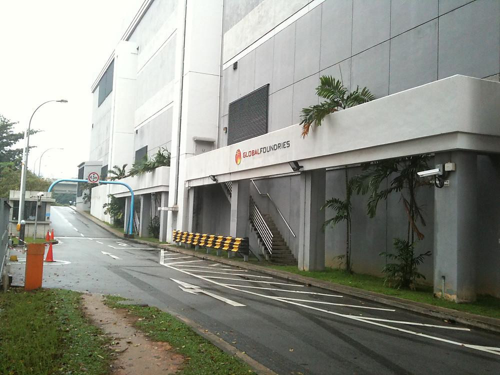
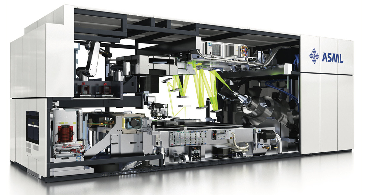
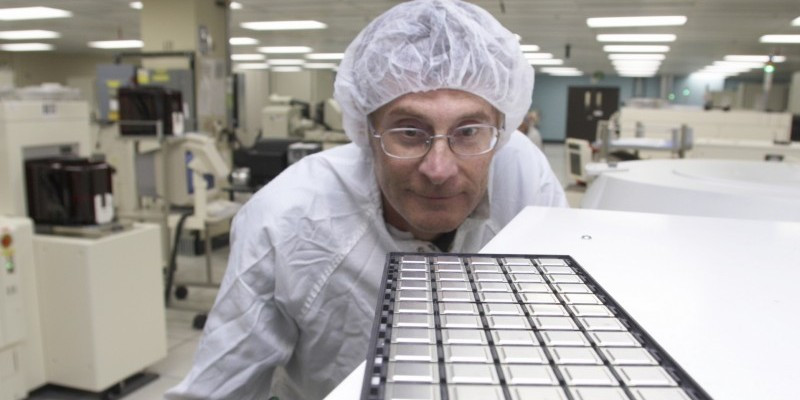
GLOBALFOUNDRIES Ceases Operations in its Chengdu Fab

GLOBALFOUNDRIES ceased all operations in its joint-venture fab in Chengdu, China. The fab opened its doors in 2018, and was supposed to mass-produce 300 mm wafers on the 22FDX technology in a 65,000 square meter facility. The company's Chinese partner, the Chengdu Municipality, had at the time boasted of investments into the fab peaking at $10 billion. The two had also announced $2 billion in initial design wins.

GloFo's announcement to cease operations and possibly withdraw from Chengdu comes hot on the heals of a separate announcement bolstering its mainland US based facilities up to US-DoD specs for secure manufacturing, a sign that the company will scale up investment into US-based facilities. GloFo's foreshadowed withdrawal from manufacturing in China is part of the ongoing "tech war" between the US and China, with the US getting American (and West-aligned) tech companies to pull manufacturing out of China, the biggest casualties of which is Huawei.

Did GlobalFoundries Give Up 7nm to Chase Silicon Photonics Manufacturing?

A Forbes report provides a fascinating peek into something that could explain GlobalFoundries stalling its 7 nm-class silicon fabrication plans, and shedding much of its offshore foundry bulk, other than just fiscal prudence. Apparently, the company has been making moves in silicon photonics, benefiting from few of the 16,000+ patents and other forms of IP it inherited from the IBM Microelectronics business acquisition from 2015. In particular, GlobalFoundries appears interested in high-bandwidth networking physical-layer applications that involve photonics and fiber-optics.

GlobalFoundries has reportedly been engaging with customers in the telecom- and data-center industries since 2016 in offering medium-range networking physical-layer solution, providing 40 Gbps bandwidths over distances of up to 10 km (without repeaters in the middle). In 2017, it partnered with Ayar Labs to develop an optical I/O chip. This solution combines Ayar's optical CMOS I/O tech with GloFo's 45 nm CMOS process to 10x the bandwidth at 1/5th the power of a copper-based I/O. By 2018, the combine qualified a platform that can push up to 100 Gbps per wavelength, and up to 800 Gbps on the client-side. By 2019, the combine developed a supercomputing chiplet co-packed with an Intel silicon as part of DARPA's PIPES (Photonics in Package for Extreme Scalability) project. With network bandwidth demand on an exponential rise with the advent of 5G, I guess you can say that the future for GloFo's silicon photonics business looks bright.

Everspin Technologies and GLOBALFOUNDRIES Extend MRAM Joint Development Agreement to 12nm

Everspin Technologies, Inc., the world's leading developer and manufacturer of Magnetoresistive RAM (MRAM), today announced an amendment of its Spin-transfer Torque (STT-MRAM) joint development agreement (JDA) with GLOBALFOUNDRIES (GF ), the world's leading specialty foundry. Everspin and GF have been partners on 40 nm, 28 nm, and 22 nm STT-MRAM development and manufacturing processes and have now updated their agreement to set the terms for a future project on an advanced 12 nm FinFET MRAM solution. Everspin is in production of discrete STT-MRAM solutions on 40 and 28 nm, including its award winning 1 Gb DDR4 device. GF recently announced it has achieved initial production of embedded MRAM (eMRAM) on its 22FDX platform.

GLOBALFOUNDRIES and GlobalWafers Sign MOU to Increase Capacity, Supply of 300mm SOI Wafers

GLOBALFOUNDRIES (GF ), the world's leading specialty foundry, and GlobalWafers Co., Ltd. (GWC), one of the top three silicon wafer manufacturers in the world, today announced they have signed a memorandum of understanding (MOU) to develop a long-term supply agreement for 300 mm silicon-on-insulator (SOI) wafers.

GWC is one of the world's leading manufacturers of 200 mm SOI wafers, and has a long and ongoing relationship with GF for supplying 200 mm SOI wafers. GWC also manufactures 300 mm SOI wafers, and under the anticipated supply agreement, GWC and GF will collaborate closely to significantly expand GWC's 300 mm SOI wafer manufacturing capacity.

Intel Rumored to be Courting GlobalFoundries for Some CPU Manufacturing

With its own silicon fabrication facilities pushed to their capacity limits, Intel is looking for third-party semiconductor foundries to share some of its supply load, and according to a WCCFTech report, its latest partner could be GlobalFoundries, which has a 14 nm-class fab in Upstate New York. If it goes through, the possible Intel-GloFo deal could see contract manufacturing commence within 2020.

GloFo's fab offers 14 nm FinFET and 12LPP, a refinement that's marketed as 12 nm. According to the report, Intel could use GloFo for manufacturing CPU dies, specifically its entry-level chips such as Core i3, Pentium, and Celeron. Intel is also known to shed its own manufacturing workload by contracting foundries for 14 nm core-logic (chipsets). In a bid to maximize 14 nm fab allocation for its CPUs, Intel also started making some of its 300-series chipsets on the older 22 nm process, which goes to show the company's appetite for 14 nm.

GLOBALFOUNDRIES and SiFive to Deliver Next Level of High Bandwidth Memory on 12LP

GLOBALFOUNDRIES (GF ) and SiFive, Inc. announced today at GLOBALFOUNDRIES Technology Conference (GTC) in Taiwan that they are working to extend high DRAM performance levels with High Bandwidth Memory (HBM2E) on GF's recently announced 12LP+ FinFET solution, with 2.5D packaging design services to enable fast time-to-market for Artificial Intelligence (AI) applications.

In order to achieve the capacity and bandwidth for data-intensive AI training applications, system designers are challenged with squeezing more bandwidth into a smaller area while maintaining a reasonable power profile. SiFive's customizable high bandwidth memory interface on GF's 12LP platform and 12LP+ solution will enable easy integration of high bandwidth memory into a single System-on-Chip (SoC) solutions to deliver fast, power-efficient data processing for AI applications in the computing and wired infrastructure markets.

GLOBALFOUNDRIES and TSMC Announce Resolution of Global Disputes Through Patent Cross-Licensing

GLOBALFOUNDRIES (GF) and TSMC today announced they are dismissing all litigation between them as well as those that involve any of their customers. The companies have agreed to a broad life-of-patents cross-license to each other's worldwide existing semiconductor patents as well as those patents that will be filed during the next ten years as both companies continue to invest significantly in semiconductor research and development. This resolution guarantees GF and TSMC freedom to operate and ensures that their respective customers will continue to have access to each foundry's complete array of technologies and services.

"We are pleased to have quickly reached this settlement that acknowledges the strength of our respective intellectual property. Today's announcement enables both of our companies to focus on innovation and to better serve our clients around the world," said Thomas Caulfield, CEO of GF. "This agreement between GF and TSMC secures GF's ability to grow and is a win for the entire semiconductor industry which is at the core of today's global economy."

GLOBALFOUNDRIES Introduces 12LP+ FinFET Solution for Cloud and Edge AI Applications

GLOBALFOUNDRIES (GF), the world's leading specialty foundry, announced today at its Global Technology Conference the availability of 12LP+, an innovative new solution for AI training and inference applications. 12LP+ offers chip designers a best-in-class combination of performance, power and area, along with a set of key new features, a mature design and production ecosystem, cost-efficient development and fast time-to-market for high-growth cloud and edge AI applications.

Derived from GF's existing 12nm Leading Performance (12LP) platform, GF's new 12LP+ provides either a 20% increase in performance or a 40% reduction in power requirements over the base 12LP platform, plus a 15% improvement in logic area scaling. A key feature is a high-speed, low-power 0.5 V SRAM bit cell that supports the fast, power-efficient shuttling of data between processors and memory, an important requirement for AI applications in the computing and wired infrastructure markets.

Globalfoundries Files Patent-infringement Lawsuits Against TSMC in the U.S. and Germany

GLOBALFOUNDRIES (GF), the world's leading specialty foundry based in the United States, today filed multiple lawsuits in the U.S. and Germany alleging that semiconductor manufacturing technologies used by Taiwan Semiconductor Manufacturing Company Ltd. (TSMC) infringe 16 GF patents. The lawsuits were filed today in the U.S. International Trade Commission (ITC), the U.S. Federal District Courts in the Districts of Delaware and the Western District of Texas, and the Regional Courts of Dusseldorf and Mannheim in Germany.

In filing the lawsuits, GF seeks orders that will prevent semiconductors produced with the infringing technology by Taiwan-based TSMC, the dominant semiconductor manufacturer, from being imported into the U.S. and Germany. These lawsuits require GF to name certain major customers of TSMC and downstream electronics companies, who, in most cases, are the actual importers of the products that incorporate the infringing TSMC technology. GF also seeks significant damages from TSMC based on TSMC's unlawful use of GF's proprietary technology in its tens of billions of dollars of sales.

GlobalFoundries and ON Semi Partner to Transfer Ownership of East Fishkill NY 300mm Fab

ON Semiconductor Corporation and GLOBALFOUNDRIES today announced that they have entered into a definitive agreement for ON Semiconductor to acquire a 300 mm fab located in East Fishkill, New York. The total consideration for the acquisition is $430 million, of which $100 million has been paid at signing of the definitive agreement, and $330 million will be paid at the end of 2022, after which ON Semiconductor will gain full operational control of the fab, and the site's employees will transition to ON Semiconductor. Completion of the transaction is subject to regulatory approval and other customary closing conditions.

The agreement allows ON Semiconductor to increase its 300 mm production at the East Fishkill fab over several years, and allows for GLOBALFOUNDRIES to transition its numerous technologies to the company's three other at-scale 300 mm sites. Under the terms of the agreement, GLOBALFOUNDRIES will manufacture 300 mm wafers for ON Semiconductor until the end of 2022. First production of 300 mm wafers for ON Semiconductor is expected to start in 2020.

GlobalFoundries to Sell its Singapore-based Fab 3E to Vanguard

GlobalFoundries has decided to exit the MEMS (microelectromechanical systems) manufacturing business by selling off its Fab 3E, located in Singapore. The foundry will be acquired lock stock and barrel by Vanguard International Semiconductor (VIS). GlobalFoundries earns USD $236 million from this sale. The transfer of operations is scheduled to take place on 31st December, 2019. Fab 3E has an installed capacity of producing 35,000 200-mm wafers per month, and specializes in MEMS and analog/mixed signal chips. Under the terms of sale, Vanguard also stands to obtain GlobalFoundries' MEMS-related IP and workforce for this facility, which continues its employment after transition. Vanguard also inherits GloFo's clientele for products made at this facility.

AMD Updates Wafer Supply Agreement with GlobalFoundries to Free Itself of "7nm Tax"

AMD in its Q4-2018 Earnings Report disclosed that it has amended its Wafer Supply Agreement (WSA) with GlobalFoundries that frees it from paying a "7 nanometer tax." Under the older version of WSA, AMD would have had to pay a penalty to GlobalFoundries if it sourced processors from any other semiconductor foundry. The company got preferential pricing in return for the exclusivity. With GlobalFoundries discontinuing development of cutting-edge processes such as 7 nm and 5 nm, it makes sense for AMD to seek out other foundry partners, such as TSMC, and an amendment to the WSA was needed. With this amendment in place, AMD can go ahead and source 7 nm dies from TSMC without paying penalties to GlobalFoundries (GloFo).

With its "Zen 2" microarchitecture, AMD is going big on multi-chip modules, in which only those components that can tangibly benefit from the switch to the 7 nm node, namely the CPU cores, would be built on 7 nm dies, called "CPU chiplets," while components that don't need the miniaturization just yet, such as the processor's memory controller, PCIe root-complex, etc., will be built on separate dies called "I/O controllers." These dies will continue to be 14 nm, and likely supplied by GloFo. Final packaging of 7 nm CPU chiplets from TSMC, and 14 nm I/O controllers from GloFo, will happen at GloFo's facilities in China or Malaysia. AMD in its amendment committed to purchasing 14 nm and 12 nm chips from GloFo between 2019 and 2021, which means the MCM approach to processors is here to stay.

GLOBALFOUNDRIES Introduces Avera Semi

GLOBALFOUNDRIES today announced the establishment of Avera Semiconductor LLC, a wholly owned subsidiary dedicated to providing custom silicon solutions for a broad range of applications. Avera Semi will leverage deep ties with GF to deliver ASIC offerings on 14/12nm and more mature technologies while providing clients new capabilities and access to alternate foundry processes at 7nm and beyond.

Avera Semi is built upon an unrivaled legacy of ASIC expertise, tapping into a world-class team that has executed more than 2,000 complex designs in its 25-year history. With more than 850 employees, annual revenues in excess of $500 million, and over $3 billion in 14nm designs in execution, Avera Semi is well positioned to serve clients developing products across a wide range of markets, including wired and wireless networking, data centers and storage, artificial intelligence and machine learning, and aerospace and defense.

GLOBALFOUNDRIES and Chengdu Realign Joint Venture Strategy

GLOBALFOUNDRIES and the Chengdu municipality signed an amendment to their investment and cooperation agreement today. Based on market condition changes, GF's recently announced renewed focus on differentiated offerings, and discussions with potential clients, the partners have decided to bypass the original phase one investment in mainstream process technology (180/130nm). It is also agreed that the project timeline will be adapted to better align capacity to meet China-based demand for differentiated offerings including GF's industry leading 22FDX technology.

With more than $2 billion of design wins and more than 50 client designs, GF's 22FDX technology is demonstrating traction as the industry's leading platform for power-optimized chips across a broad range of high-growth applications such as automotive, 5G connectivity and the Internet of Things (IoT). GF's Chinese clients are beginning to adopt the technology at GF's advanced manufacturing site in Dresden, Germany, including seven customers and more than nine products in various stages of manufacturing ramp.

"We have a long-term relationship with GF and the 22FDX with its low power is very suitable for our various products, including AI and security," said Min Li, CEO of Rockchip. "Once we achieve the right level of readiness, we look forward to ramping our production closer to home in China."

Analyst Firm Susquehanna: "Intel Lost its Manufacturing Leadership"

Intel was once the shining star in the semiconductor manufacturing industry, with a perfectly integrated, vertical product design and manufacturing scheme. Intel was one of the few companies in the world to be able to both develop its architectures and gear their manufacturing facilities to their design characteristics, ensuring a perfect marriage of design and manufacturing. However, not all is rosy on that field, as we've seen; AMD itself also was a fully integrated company, but decided to spin-off its manufacturing arm so as to survive - thus creating GLOBALFOUNDRIES.But Intel was seen as many as the leader in semiconductor manufacturing, always at the cutting edge of - well - Moore's Law, named after Intel's founding father Gordon Moore. Now, Mehdi Hosseini, an analyst with Susquehanna, has gone on to say that the blue giant has effectively lost its semiconductor leadership. And it has, in a way, even if its 10 nm (which is in development hell, so to speak) is technically more advanced than some 7 nm implementations waiting to be delivered to market by its competitors. However, there's one area where Intel will stop being able to claim leadership: manufacturing techniques involving EUV (Extreme UltraViolet).

AMD Fast-tracks 7nm "Navi" GPU to Late-2018 Alongside "Zen 2" CPU

AMD is unique in the world of computing as the only company with both high-performance CPU and GPU products. For the past several years we have been executing our multi-generational leadership product and architectural roadmap. Just in the last 18 months, we successfully introduced and ramped our strongest set of products in more than a decade and our business has grown dramatically as we gained market share across the PC, gaming and datacenter markets.

The industry is at a significant inflection point as the pace of Moore's Law slows while the demand for computing and graphics performance continues to grow. This trend is fueling significant shifts throughout the industry and creating new opportunities for companies that can successfully bring together architectural, packaging, system and software innovations with leading-edge process technologies. That is why at AMD we have invested heavily in our architecture and product roadmaps, while also making the strategic decision to bet big on the 7nm process node. While it is still too early to provide more details on the architectural and product advances we have in store with our next wave of products, it is the right time to provide more detail on the flexible foundry sourcing strategy we put in place several years ago.

AMD Chip Manufacturing to Lay Solely With TSMC On, After 7 nm - And Why It's not a Decision, but a Necessity

It's been a tumultuous few days for AMD, as the company has seen Jim Anderson, Computing and Graphics Group leader after the departure of Raja Koduri, leave the company, at a time of soaring share value for the company (hitting $25.26 and leaving short positions well, short, by $2.67 billion.) However, there's one particular piece of news that is most relevant for the company: Globalfoundries' announcement to stop all ongoing development on the 7 nm node.

This is particularly important for a variety of reasons. The most important one is this: Globalfoundries' inability to execute on the 7 nm node leaves AMD fully free to procure chips and technology from competing foundries. If you remember, AMD's spin-off of GlobalFoundries left the former with the short end of the stick, having to cater to GlobalFoundries' special pricing, and paying for the privilege of accessing other foundries' inventories. Of course, the Wafer Supply Agreement (WSA) that is in place will have to be amended - again - but the fact is this: AMD wants 7 nm products, and GlobalFoundries can't provide.
To the forumites: this piece is marked as an editorial

GlobalFoundries Puts its 7 nm Program on Hold Indefinitely

GLOBALFOUNDRIES today announced an important step in its transformation, continuing the trajectory launched with the appointment of Tom Caulfield as CEO earlier this year. In line with the strategic direction Caulfield has articulated, GF is reshaping its technology portfolio to intensify its focus on delivering truly differentiated offerings for clients in high-growth markets.

GF is realigning its leading-edge FinFET roadmap to serve the next wave of clients that will adopt the technology in the coming years. The company will shift development resources to make its 14/12nm FinFET platform more relevant to these clients, delivering a range of innovative IP and features including RF, embedded memory, low power and more. To support this transition, GF is putting its 7nm FinFET program on hold indefinitely and restructuring its research and development teams to support its enhanced portfolio initiatives. This will require a workforce reduction, however a significant number of top technologists will be redeployed on 14/12nm FinFET derivatives and other differentiated offerings.

GLOBALFOUNDRIES Surpasses $2 Billion in Design Win Revenue on 22FDX Technology

GLOBALFOUNDRIES today announced that the company's 22nm FD-SOI (22FDX ) technology has delivered more than two billion dollars of client design win revenue. With more than 50 total client designs, 22FDX is proving to be the industry's leading platform for power-optimized chips across a broad range of high-growth applications such as automotive, 5G connectivity and the Internet of Things (IoT).

For clients who need significant reductions in power and die size relative to a traditional bulk CMOS process, 22FDX offers the industry's lowest operating voltage, delivering up to 500MHz frequencies at only 0.4 volts. The technology also delivers efficient single-chip integration of RF, transceiver, baseband, processor, and power management components, providing an unparalleled combination of high performance RF and mmWave functionality with low-power, high density logic for devices that require long-lasting battery life, increased processing capability, and connectivity.

"At Synaptics, as we expand upon our industry-leading mobile and PC businesses to include delivering new and innovative products that address the booming IoT market, we require the best available technologies to enable us to deliver top-notch solutions including voice and multimedia processing capabilities for our customers," said Rick Bergman, President and CEO at Synaptics. "GF's 22FDX technology delivers a potent mix of low static and dynamic power along with excellent performance to give us a great platform for our world-class products."

Challenges With 7 nm, 5 nm EUV Technologies Could Lead to Delays In Process' TTM

Semiconductor manufacturers have been historically bullish when it comes to the introduction of new manufacturing technologies. Intel, AMD (and then Globalfoundries), TSMC, all are companies who thrive in investors' confidence: they want to paint the prettiest picture they can in terms of advancements and research leadership, because that's what attracts investment, and increased share value, and thus, increased funds to actually reach those optimistic goals.

However, we've seen in recent years how mighty Intel itself has fallen prey to unforeseen complications when it comes to advancements of its manufacturing processes, which saw us go from a "tick-tock" cadence of new architecture - new manufacturing process, to the introduction of 14 nm ++ processes. And as Intel, Globalfoundries and TSMC race towards sub 7-nm manufacturing processes with 250 mm wafers and EUV usage, things aren't getting as rosy as the ultraviolet moniker would make us believe.

GLOBALFOUNDRIES Appoints Industry Veteran Tom Caulfield as New CEO

After more than four years as chief executive officer of GLOBALFOUNDRIES, Sanjay Jha will hand over the company's top position to Dr. Thomas Caulfield, senior vice president and general manager and a highly-respected industry veteran.

Caulfield joined GF in 2014 following a successful career with an impressive track record of results spanning engineering, management, operational leadership and global executive experience with leading technology companies including 17 years at IBM in a variety of senior leadership roles. During his tenure at GF, he successfully built and ramped the company's new 14nm production facility in upstate New York, the most advanced foundry facility and one of the largest public-private partnerships in the United States.

Globalfoundries: 7 nm to Enable up to 2.7x Smaller Dies, 5 GHz CPUs

Globalfoundries' Chief Technical Officer, Gary Patton, talked about the future he believes can be possible in future manufacturing processes, calling for particular attention towards the next step in the ladder at 7 nm. Apparently, the 7 nm process at Globalfoundries has received a shot in the arm from the integration of ex IBM engineering specialists (remember that IBM practically paid Globalfoundries to take its manufacturing division of its hands), and the company now expects better than foreseen technical specs and achievements of its 7 nm process.

While a move from 14 nm to 7 nm was expected to provide, at the very best, a halving in the actual size of a chip manufactured in 7 nm compared to 14 nm, Gary Patton is now saying that the are should actually be reduced by up to 2.7 times the original size. To put that into perspective, AMD's 1000 series processors on the Zeppelin die and 14 nm process, which come in at 213 mm² for the full, 8-core design, could be brought down to just 80 mm² instead. AMD could potentially use up that extra die space to either build in some overprovisioning, should the process still be in its infancy and yields need a small boost; or cram it with double the amount of cores and other architectural improvements, and still have chips that are smaller than the original Zen dies.

AMD To Change Suppliers for Vega 20 GPUs on 7nm, HBM2 Packaging for Vega 11

AMD's RX Vega supply has seen exceedingly limited quantities available since launch. This has been due to a number of reasons, though the two foremost that have been reported are: increased demand from cryptocurrency miners, who are looking towards maximizing their single node hashrate density through Vega's promising mining capabilities; and yield issues with AMD's Vega 10 HBM2 packaging partner, Advanced Semiconductor Engineering (ASE). It's expected that chip yield for Vega 10 is also lower per se, due to it having a 484 mm² die, which is more prone to defects than a smaller one, thus reducing the amount of fully-enabled GPUs.

AMD's production partner, GlobalFoundries, has historically been at the center of considerations on AMD's yield problems. That GlobalFoundries is seemingly doing a good job with Ryzen may not be much to say: those chips have incredibly small die sizes (192 mm²) for their number of cores. It seems that Global Foundries only hits problems with increased die sizes and complexity (which is, unfortunately for AMD, where it matters most).

GLOBALFOUNDRIES on Track to Deliver Leading-Performance 7nm FinFET Technology

GLOBALFOUNDRIES today announced the availability of its 7nm Leading-Performance (7LP) FinFET semiconductor technology, delivering a 40 percent generational performance boost to meet the needs of applications such as premium mobile processors, cloud servers and networking infrastructure. Design kits are available now, and the first customer products based on 7LP are expected to launch in the first half of 2018, with volume production ramping in the second half of 2018.

In September 2016, GF announced plans to develop its own 7nm FinFET technology leveraging the company's unmatched heritage of manufacturing high-performance chips. Thanks to additional improvements at both the transistor and process levels, the 7LP technology is exceeding initial performance targets and expected to deliver greater than 40 percent more processing power and twice the area scaling than the previous 14nm FinFET technology. The technology is now ready for customer designs at the company's leading-edge Fab 8 facility in Saratoga County, N.Y.

"Our 7nm FinFET technology development is on track and we are seeing strong customer traction, with multiple product tapeouts planned in 2018," said Gregg Bartlett, senior vice president of the CMOS Business Unit at GF. "And, while driving to commercialize 7nm, we are actively developing next-generation technologies at 5nm and beyond to ensure our customers have access to a world-class roadmap at the leading edge."

IBM Research Alliance Builds New Transistor for 5 nm Technology

IBM, its Research Alliance partners GLOBALFOUNDRIES and Samsung, and equipment suppliers have developed an industry-first process to build silicon nanosheet transistors that will enable 5 nanometer (nm) chips. The details of the process will be presented at the 2017 Symposia on VLSI Technology and Circuits conference in Kyoto, Japan. In less than two years since developing a 7 nm test node chip with 20 billion transistors, scientists have paved the way for 30 billion switches on a fingernail-sized chip.

The resulting increase in performance will help accelerate cognitive computing, the Internet of Things (IoT), and other data-intensive applications delivered in the cloud. The power savings could also mean that the batteries in smartphones and other mobile products could last two to three times longer than today's devices, before needing to be charged.
Return to Keyword Browsing
Apr 18th, 2024 18:08 EDT change timezone

New Forum Posts

Popular Reviews

Controversial News Posts