News Posts matching #GLOBALFOUNDRIES

Return to Keyword Browsing

AMD to Continue Working With TSMC, GLOBALFOUNDRIES on 7 nm Ryzen

In the Q&A section of their 2017 Financial Analyst Day, AMD CEO Lisa Su answered an enquiry from a Deutsche-bank questioner regarding the company's aggressive 7 nm plan for their roadmap, on which AMD seems to be balancing its process shrinkage outlook for the foreseeable future. AMD will be developing their next Zen architecture revisions on 7 nm, alongside a push for 7 nm on their next-generation (or is that next-next generation?) Navi architecture. This means al of AMD's products, consumer, enterprise, and graphics, will be eventually built on this node. This is particularly interesting considering AMD's position with GLOBALFOUNDRIES, with which AMD has already had many amendments to their Wafer Supply Agreement, a remain of AMD's silicon production division spin-off, the latest of which runs from 2016 to 2020.

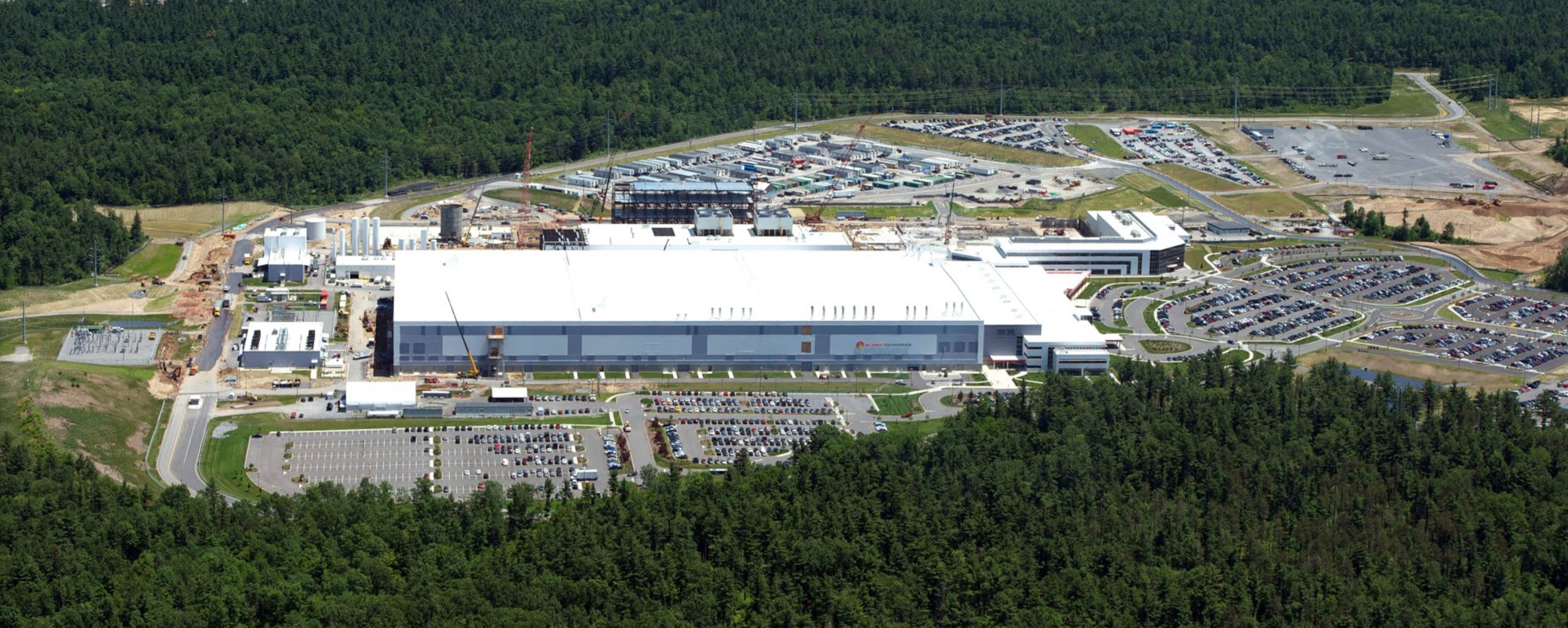
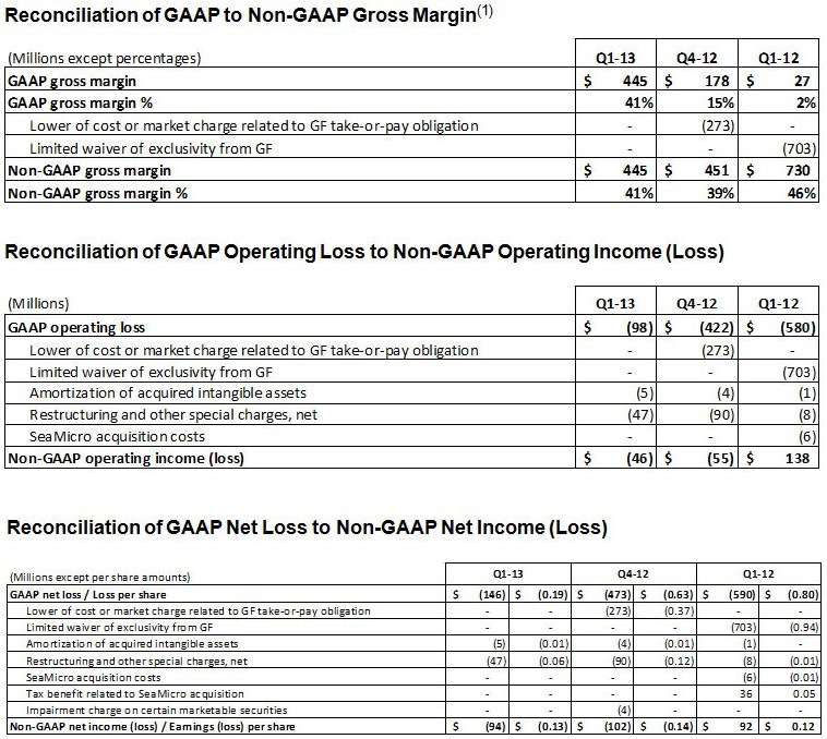
As it is, AMD has to pay GLOBALFOUNDRIES for its wafer orders that go to other silicon producers (in this case, TSMC), in a quarterly basis since the beginning of 2017, based on the volume of certain wafers purchased from another wafer foundry. In addition, AMD has annual wafer purchase targets from 2016 through the end of 2020, fixed wafer prices for 2016, and a framework for yearly wafer pricing in this amendment, so the company is still bleeding money to GLOBALFOUNDRIES. However, AMD is making the correct decision in this instance, I'd wager, considering GLOBALFOUNDRIES' known difficulties in delivering their process nodes absent of quirks.

GLOBALFOUNDRIES Cutting Staff Through Earlier Retirements

It would seem business is not as usual for GLOBALFOUNDRIES, which started as the spin-off from AMD's manufacturing arm way back on March 2, 2009. Blaming the capricious chip market's fluctuations, the company is looking to divest longtime employees in all three of its U.S. semiconductor manufacturing plants, including Essex Junction, which it acquired from IBM in 2015 by... receiving a $1.5 billion payment from the company. And as part of the deal, GLOBALFOUNDRIES agreed to be IBM's exclusive provider of semiconductor chips through 2025.

"We go through these ebbs and flows," Spokesman Jim Keller said Wednesday. "Right now we're at a point where some customers delayed their orders. We're in a period where we don't have as much business." The "voluntary separation" program is part of a larger cost cutting initiative that will look for other efficiency savings as well, though "layoffs are also a possibility". Keller would not say how many of GLOBALFOUNDRIES' 2,800 employees at Essex Junction are eligible for the early retirement program. Most of the workers eligible are in "support roles," such as administrative, sales or finance.

Rambus Introduces High Bandwidth Memory PHY on GlobalFoundries FX-14

Rambus Inc. today announced the availability of its High Bandwidth Memory (HBM) Gen2 PHY developed for GLOBALFOUNDRIES high-performance FX-14 ASIC Platform. Built on the GLOBALFOUNDRIES 14nm FinFET (14LPP) process technology, the Rambus HBM PHY is aimed at networking and data center applications and designed for systems that require low latency and high bandwidth memory. This PHY is fully compliant with the JEDEC HBM2 standard and supports data rates up to 2000 Mbps per data pin, enabling a total bandwidth of 256 GB/s to meet the needs of today's most data-intensive tasks.

"Data center needs are continuously changing and we are at the forefront of delivering memory interface technology designed to meet today's most demanding workloads," said Luc Seraphin, senior vice president and general manager of the Rambus Memory and Interfaces division. "Through our collaboration with GLOBALFOUNDRIES, we are delivering a comprehensive and robust solution for high-performance data center and networking applications. Our HBM offering will allow data center solution developers to bring high performance memory closer to the CPU, thus reducing latency and improving the system throughput."

AMD Reports Fourth Quarter and Annual 2016 Financial Results

AMD (NASDAQ: AMD) today announced revenue for the fourth quarter of 2016 of $1.11 billion, operating loss of $3 million and net loss of $51 million, or $0.06 per share. Non-GAAP(1) operating income was $26 million, non-GAAP(1) net loss was $8 million and non-GAAP(1) loss per share was $0.01.

"We met our strategic objectives in 2016, successfully executing our product roadmaps, regaining share in key markets, strengthening our financial foundation, and delivering annual revenue growth," said Dr. Lisa Su, AMD president and CEO. "As we enter 2017, we are well positioned and on-track to deliver our strongest set of high-performance computing and graphics products in more than a decade."

AMD's Q3 2016 Earnings Call - Revenue is Up, Debt is Down

AMD today released their earnings call for 3Q 2016, giving us some interesting tidbits in regards to their financial robustness. The balance of AMD's economics seems to be pending towards better execution, and, coeteris paribus, a much better outlook for the coming quarters, after the monumental missteps in the past that almost threw AMD under the proverbial bus. Reception for the results seems to be a tangled mess, however, with some sides claiming that AMD beat expectations, while others prefer to draw attention to AMD's 2% stock decline since the report was outed.

AMD posted revenue of $1,307 million, up 27% sequentially and 23% year-over-year. This revenue was distributed unevenly through AMD's divisions, though. "Computing and Graphics" segment revenue was $472 million, up 9% from Q2 2016, primarily due to increased GPU sales (where Polaris picked up the grunt of the work, being responsible for 50% of AMD's GPU revenue), offset by lower sales of client desktop processors and chipsets; whereas "Enterprise, Embedded and Semi-Custom" segment revenue was $835 million, up 41% sequentially, primarily due to record semi-custom SoC sales (such as those found in Microsoft's XBOX One and Sony's PS4 and upcoming PS4 Pro).

GLOBALFOUNDRIES Announces its 7 nm FinFET Technology

GLOBALFOUNDRIES today announced plans to deliver a new leading-edge 7nm FinFET semiconductor technology that will offer the ultimate in performance for the next era of computing applications. This technology provides more processing power for data centers, networking, premium mobile processors, and deep learning applications.

GLOBALFOUNDRIES' new 7nm FinFET technology is expected to deliver more than twice the logic density and a 30 percent performance boost compared to today's 16/14nm foundry FinFET offerings. The platform is based on an industry-standard FinFET transistor architecture and optical lithography, with EUV compatibility at key levels. This approach will accelerate the production ramp through significant re-use of tools and processes from the company's 14nm FinFET technology, which is currently in volume production at its Fab 8 campus in Saratoga County, N.Y. GLOBALFOUNDRIES plans to make an additional mutli-billion dollar investment in Fab 8 to enable development and production for 7nm FinFET.

"The industry is converging on 7nm FinFET as the next long-lived node, which represents a unique opportunity for GLOBALFOUNDRIES to compete at the leading edge," said GLOBALFOUNDRIES CEO Sanjay Jha. "We are well positioned to deliver a differentiated 7nm FinFET technology by tapping our years of experience manufacturing high-performance chips, the talent and know-how of our former IBM Microelectronics colleagues and the world-class R&D pipeline from our research alliance. No other foundry can match this legacy of manufacturing high-performance chips."

GlobalFoundries Announces its 12 nm FD-SOI Silicon Fabrication Node

GLOBALFOUNDRIES today unveiled a new 12nm FD-SOI semiconductor technology, extending its leadership position by offering the industry's first multi-node FD-SOI roadmap. Building on the success of its 22FDXTM offering, the company's next-generation 12FDXTM platform is designed to enable the intelligent systems of tomorrow across a range of applications, from mobile computing and 5G connectivity to artificial intelligence and autonomous vehicles.

As the world becomes more and more integrated through billions of connected devices, many emerging applications demand a new approach to semiconductor innovation. The chips that make these applications possible are evolving into mini-systems, with increased integration of intelligent components including wireless connectivity, non-volatile memory, and power management-all while driving ultra-low power consumption. GLOBALFOUNDRIES' new 12FDX technology is specifically architected to deliver these unprecedented levels of system integration, design flexibility, and power scaling.

AMD Announces Amendment to Wafer Supply Agreement With GLOBALFOUNDRIES

AMD announced that it has entered into a long-term amendment to its Wafer Supply Agreement (WSA) with GLOBALFOUNDRIES Inc. (GF) for the period from Jan. 1, 2016 to Dec. 31, 2020. "The five-year amendment further strengthens our strategic manufacturing relationship with GLOBALFOUNDRIES while providing AMD with increased flexibility to build our high-performance product roadmap with additional foundries in the 14 nm and 7 nm technology nodes," said Dr. Lisa Su, AMD president and CEO. "Our goal is for AMD to have continued access to leading-edge foundry process technologies enabling us to build multiple generations of great products for years to come."

GLOBALFOUNDRIES' Fab 8 in Malta, N.Y. is playing a significant role in providing leading-edge capacity for AMD's graphics and processor products, including the recently launched AMD Radeon Polaris GPUs and upcoming "Zen"-based processors.

GlobalFoundries to Skip 10 nm and Jump Straight to 7 nm

Silicon fabrication company GlobalFoundries is reportedly planning to skip development of the 10 nanometer (nm) process, and is aiming to jump straight to 7 nm. The company currently operates a 14 nm FinFET node. In 2015 the company acquired semiconductor manufacturing assets from IBM, and is using them to fast-track its development. When it's ready, the 7 nm node will offer both optical and EUV (extreme ultra-violet) lithography. Driving the EUV product is an IBM 3300 EUV fabricator at the company's advanced patterning center, in its Albany, New York fab.

GLOBALFOUNDRIES Achieves 14nm FinFET Technology Success for Next-Gen AMD Product

GLOBALFOUNDRIES today announced it has demonstrated silicon success on the first AMD (NASDAQ: AMD) products using GLOBALFOUNDRIES' most advanced 14nm FinFET process technology. As a result of this milestone, GLOBALFOUNDRIES' silicon-proven technology is planned to be integrated into multiple AMD products that address the growing need for high-performance, power-efficient compute and graphics technologies across a broad set of applications, from personal computers to data centers to immersive computing devices.

AMD has taped out multiple products using GLOBALFOUNDRIES' 14nm Low Power Plus (14LPP) process technology and is currently conducting validation work on 14LPP production samples. Today's announcement represents another significant milestone towards reaching full production readiness of GLOBALFOUNDRIES' 14LPP process technology, which will reach high-volume production in 2016. The 14LPP platform taps the benefits of three-dimensional, fully-depleted FinFET transistors to enable customers like AMD to deliver more processing power in a smaller footprint for applications that demand the ultimate in performance.

GLOBALFOUNDRIES Launches Industry's First 22nm FD-SOI Technology Platform

GLOBALFOUNDRIES today launched a new semiconductor technology developed specifically to meet the ultra-low-power requirements of the next generation of connected devices. The "22FDX" platform delivers FinFET-like performance and energy-efficiency at a cost comparable to 28 nm planar technologies, providing an optimal solution for the rapidly evolving mainstream mobile, Internet-of-Things (IoT), RF connectivity and networking markets.

While some applications require the ultimate performance of three-dimensional FinFET transistors, most wireless devices need a better balance of performance, power consumption and cost. 22FDX provides the best path for cost-sensitive applications by leveraging the industry's first 22nm two-dimensional, fully-depleted silicon-on-insulator (FD-SOI) technology. It offers industry's lowest operating voltage at 0.4 volt, enabling ultra-low dynamic power consumption, less thermal impact, and smaller end-product form-factors. The 22FDX platform delivers a 20 percent smaller die size and 10 percent fewer masks than 28nm, as well as nearly 50 percent fewer immersion lithography layers than foundry FinFET.

"The 22FDX platform enables our customers to deliver differentiated products with the best balance of power, performance and cost," said Sanjay Jha, chief executive officer of GLOBALFOUNDRIES. "In an industry first, 22FDX provides real-time system software control of transistor characteristics: the system designer can dynamically balance power, performance, and leakage. Additionally, for RF and analog integration, the platform delivers best scaling combined with highest energy efficiency."

GLOBALFOUNDRIES Completes Acquisition of IBM Microelectronics Business

GLOBALFOUNDRIES today announced that it has completed its acquisition of IBM's Microelectronics business. With the acquisition, GLOBALFOUNDRIES gains differentiated technologies to enhance its product offerings in key growth markets, from mobility and Internet of Things (IoT) to Big Data and high-performance computing. The deal strengthens the company's workforce, adding decades of experience and expertise in semiconductor development, device expertise, design, and manufacturing. And the addition of more than 16,000 patents and applications makes GLOBALFOUNDRIES the holder of one of the largest semiconductor patent portfolios in the world.

"Today we have significantly enhanced our technology development capabilities and reinforce our long-term commitment to investing in R&D for technology leadership," said Sanjay Jha, chief executive officer of GLOBALFOUNDRIES. "We have added world-class technologists and differentiated technologies, such as RF and ASIC, to meet our customers' needs and accelerate our progress toward becoming a foundry powerhouse." Through the addition of some of the brightest and most innovative scientists and engineers in the semiconductor industry, GLOBALFOUNDRIES solidifies its path to advanced process technologies at 10 nm, 7 nm, and beyond.

GLOBALFOUNDRIES To Acquire IBM's Microelectronics Business

IBM and GLOBALFOUNDRIES today announced that they have signed a Definitive Agreement under which GLOBALFOUNDRIES plans to acquire IBM's global commercial semiconductor technology business, including intellectual property, world-class technologists and technologies related to IBM Microelectronics, subject to completion of applicable regulatory reviews. GLOBALFOUNDRIES will also become IBM's exclusive server processor semiconductor technology provider for 22 nanometer (nm), 14 nm and 10 nm semiconductors for the next 10 years.

The Agreement, once closed, enables IBM to further focus on fundamental semiconductor research and the development of future cloud, mobile, big data analytics, and secure transaction-optimized systems. IBM continues its previously announced $3 billion investment over five years for semiconductor technology research to lead in the next generation of computing. GLOBALFOUNDRIES will have primary access to the research that results from this investment through joint collaboration at the Colleges of Nanoscale Science and Engineering (CNSE), SUNY Polytechnic Institute, in Albany, N.Y.

GLOBALFOUNDRIES Names Tom Caulfield as GM of its New York Fab

GLOBALFOUNDRIES, a leading provider of advanced semiconductor manufacturing technology, today appointed Dr. Thomas Caulfield as senior vice president and general manager of the company's latest leading-edge 300mm semiconductor wafer manufacturing facility (Fab 8), located in Saratoga County, NY. Caulfield, an accomplished industry leader with more than 20 years of technical and global executive experience, will lead the operations, expansion and ramp of semiconductor manufacturing production at Fab 8, where GLOBALFOUNDRIES supports customers on the world's most advanced semiconductor manufacturing technology platforms including 28 nanometer (nm), 20 nm, and the recently announced 14 nm FinFET platform.

"We are expanding our Fab 8 manufacturing campus, strengthening strategic partnerships, and deepening customer relationships so we can offer our customers leading-edge technology and a more flexible and cost-effective way of doing business," said GLOBALFOUNDRIES CEO Sanjay Jha. "Tom is a proven and respected industry leader with more than two decades of semiconductor technology and manufacturing experience and we are excited to have him join our team to drive the next phase of growth at Fab 8."

Toshiba Joins GLOBALSOLUTIONS Ecosystem as Worldwide ASIC Partner

GLOBALFOUNDRIES today announced that Toshiba Corporation will join the company's GLOBALSOLUTIONS ecosystem of partners. As a worldwide ASIC partner, Toshiba will enable its Fit Fast Structured Array (FFSA) and ASIC solutions based upon GLOBALFOUNDRIES' technologies and services for customers across the globe. The agreement includes participation on multi-project wafer (MPW) runs and production wafers covering the whole portfolio of GLOBALFOUNDRIES technologies, including leading-edge process nodes.

Initially, the partnership will focus on implementations of Toshiba's FFSAs manufactured with GLOBALFOUNDRIES' 65nm and 40nm low-power process technologies, with 28nm arrays to follow. Toshiba's FFSA products-including libraries and intellectual property (IP)-allow customers to reduce development time and costs by customizing existing base wafers, choosing from a number of design platforms at GLOBALFOUNDRIES. For higher-volume applications, customers can work with Toshiba's libraries to develop fully custom system-on-chips (SoCs). With an initial product completed, customers can then leverage the embedded FFSA technology to provide quick-turn derivative products, with much lower development costs.

Samsung and GLOBALFOUNDRIES to Deliver Multi-Sourced 14 nm FinFET Offering

Samsung Electronics Co., Ltd. and GLOBALFOUNDRIES today announced a new strategic collaboration to deliver global capacity for 14 nanometer (nm) FinFET process technology. For the first time, the industry's most advanced 14 nm FinFET technology will be available at both Samsung and GLOBALFOUNDRIES, giving customers the assurance of supply that can only come from true design compatibility at multiple sources across the globe.

The new collaboration will leverage the companies' worldwide leading-edge semiconductor manufacturing capabilities, with volume production at Samsung's fabs in Hwaseong, Korea and Austin, Texas, as well as GLOBALFOUNDRIES' fab in Saratoga, New York.

AMD Amends Wafer Supply Agreement With GLOBALFOUNDRIES

AMD today announced that it amended its Wafer Supply Agreement (WSA) with GLOBALFOUNDRIES Inc. for 2014. Under the terms of the amendment, AMD and GLOBALFOUNDRIES agreed on purchase commitments for 2014 and established fixed pricing and other terms of the WSA which apply to products AMD will purchase from GLOBALFOUNDRIES.

Under this amendment AMD expects to pay GLOBALFOUNDRIES approximately $1.2 billion in 2014. These purchases contemplate AMD's current PC market expectations and the manufacturing of certain Graphics Processor Units (GPUs) and semi-custom game console products at GLOBALFOUNDRIES in 2014. The 2014 amendment does not impact AMD's 2014 financial goals including gross margin.

Toshiba to Collaborate with GLOBALFOUNDRIES on FFSA Manufacturing

Toshiba Corporation today announced that the company will collaborate with GLOBALFOUNDRIES in the manufacture of Toshiba's FFSA (Fit Fast Structured Array) products. Toshiba will expand its FFSA business through production at GLOBALFOUNDRIES's fabs. Initial products will be manufactured using GLOBALFOUNDRIES 65nm-LPe and 40nm-LP processes, with plans to extend the collaboration to the company's 28nm High-K Metal Gate (HKMG) technology.

Toshiba's FFSA products, developed in collaboration with BaySand Inc. of the U.S., can be configured simply by customizing the design of a few metal layers. This customization process secures a much shorter development turn-around-time than with conventional ASIC devices, and satisfies increasing market needs for high performance, high specifications and low power technologies. At a time of ever-shorter product life cycles, time available for development is at a premium, and solutions that meet demand and allow tweaking of the specifications until just before the start of trial production increase the freedom and flexibility of developers.

GLOBALFOUNDRIES Announces New Chief Executive to Lead Next Phase of Growth

Building on the successful track record of its first five years in the semiconductor industry and its continued commitment to build out its global network of manufacturing facilities, GLOBALFOUNDRIES announced today, from its new offices in Silicon Valley, Sanjay Jha has been appointed as the company's new Chief Executive Officer. Jha has served as CEO of Motorola Mobility Inc. and as the COO of Qualcomm Inc.

Ajit Manocha, who served as an advisor to the company's shareholder prior to being appointed CEO of GLOBALFOUNDRIES in mid-2011, will return to that role and will work closely with Jha on his transition.

Micron Technology Appoints Rajan Rajgopal as Vice President of Quality

Micron Technology, Inc. (Nasdaq:MU), today announced that the company has named Rajan Rajgopal, vice president of Quality. Rajgopal will be responsible for overseeing all aspects of Micron's quality systems including manufacturing, customer program management and product ramps. He brings more than 25 years of experience to Micron and most recently served as the vice president of Global Quality and Customer Enablement for GLOBALFOUNDRIES in Singapore.

"Micron continues to evolve as a memory business driven by systems-level solutions, and quality plays a heightened role in serving our valued customers," said Micron President Mark Adams. "We are excited to have Rajan join our team and leverage his experience in serving our customers in an increasingly diversified set of application segments."

RockChip Builds SoCs on GlobalFoundries' 28 nm HKMG Process

GLOBALFOUNDRIES and Fuzhou Rockchip Electronics Co., Ltd. today announced that Rockchip's next-generation mobile processors are ramping to production on GLOBALFOUNDRIES' 28 nm High-K Metal Gate (HKMG) process technology. Based on a multi-core ARM Cortex-A9 design, the RK3188 and RK3168 chips are optimized for tomorrow's high-performance, low-cost tablets that require long-lasting battery life (see product specifications in annex).

The combination of Rockchip's design and GLOBALFOUNDRIES' 28 nm HKMG process technology resulted in a mainstream tablet System-on-Chip (SoC) capable of operating at up to 1.8 GHz performance, while still maintaining the power efficiency expected by mobile device users. The chips began sampling to OEMs in early 2013 and are now ramping to support a wide range of manufacturers.

GLOBALFOUNDRIES Accelerates Adoption of 20nm-LPM and 14nm-XM FinFET Processes

At next week's 50th Design Automation Conference (DAC) in Austin, Texas, GLOBALFOUNDRIES will unveil a comprehensive set of certified design flows to support its most advanced manufacturing processes. The flows, jointly developed with the leading EDA providers, offer robust support for implementing designs in the company's 20nm low power process and its leading-edge 14nm-XM FinFET process. Working closely with Cadence Design Systems, Mentor Graphics and Synopsys, GLOBALFOUNDRIES has developed the flows to address the most pressing design challenges, including support for analog/mixed signal (AMS) design, and advanced digital designs, both with demonstration of the impact of double patterning on the flow.

The GLOBALFOUNDRIES design flows work with its process design kits (PDKs) to provide real examples that demonstrate the entire flow. The user can download the design database, the PDK, detailed documentation and multi-vendor scripts to learn how to set up and use the GLOBALFOUNDRIES design flow. The flows use open source examples and provide the customer with working, executable and customizable flows.

Globalfoundries and Infineon Collaborate for 40 nm Embedded Flash Process

Infineon Technologies and GLOBALFOUNDRIES Inc. today announced a joint technology development and production agreement for 40 nanometer (nm) embedded flash (eFlash) process technology. The cooperation will focus on technology development based on Infineon's eFlash cell design and manufacturing of automotive and security microcontrollers (MCUs) with 40nm process structures. Production of the next generation 40nm eFlash MCUs will take place at different GLOBALFOUNDRIES sites, initially in Singapore with subsequent transfer to its site in Dresden, Germany.

"Next generation embedded Flash microcontrollers with 40nm process structures will further enhance our competitive strength in the automotive as well as chip card and security markets," says Arunjai Mittal, Member of the Management Board of Infineon Technologies. "We trust in GLOBALFOUNDRIES with their excellent manufacturing background and sites on different continents to fulfill Infineon's stringent quality, infrastructure security and business continuity requirements."

AMD Reports 2013 First Quarter Results

AMD (NYSE:AMD) today announced revenue for the first quarter of 2013 of $1.09 billion, an operating loss of $98 million and a net loss of $146 million, or $0.19 per share. The company reported a non-GAAP operating loss of $46 million and a non-GAAP net loss of $94 million, or $0.13 per share.

"Our first quarter results reflect our disciplined operational execution in a difficult market environment," said Rory Read, AMD president and CEO. "We have largely completed our restructuring and are now focused on delivering a powerful set of new products that will accelerate our business in 2013. We will continue to diversify our portfolio and attack high-growth markets like dense server, ultra low-power client, embedded and semi-custom solutions to create the foundation for sustainable financial returns."

Hybrid Memory Cube Consortium Finalizes Specifications

More than 100 developer and adopter members of the Hybrid Memory Cube Consortium (HMCC) today announced they've reached consensus for the global standard that will deliver a much-anticipated, disruptive memory computing solution. Developed in only 17 months, the final specification marks the turning point for designers in a wide range of segments-from networking and high-performance computing, to industrial and beyond-to begin designing Hybrid Memory Cube (HMC) technology into future products.

A major breakthrough with HMC is the long-awaited utilization of advanced technologies to combine highperformance logic with state-of-the-art DRAM. With this first HMC milestone reached so quickly, consortium members have elected to extend their collaborative effort to achieve agreement on the next generation of HMC interface standards.
Return to Keyword Browsing
Apr 26th, 2024 07:44 EDT change timezone

New Forum Posts

Popular Reviews

Controversial News Posts