News Posts matching #HBM2

Return to Keyword Browsing

Huawei Aims to Develop Homegrown HBM Memory Amidst US Sanctions

According to The Information, in a strategic maneuver to circumvent the constraints imposed by US sanctions, Huawei is accelerating efforts to establish domestic production capabilities for High Bandwidth Memory (HBM) within China. This move addresses the limitations that have hampered the company's advancements in AI and high-performance computing (HPC) sectors. HBM technology plays a pivotal role in enhancing the performance of AI and HPC processors by mitigating memory bandwidth bottlenecks. Recognizing its significance, Huawei has assembled a consortium comprising memory manufacturers backed by the Chinese government and prominent semiconductor companies like Fujian Jinhua Integrated Circuit. This consortium is focused on advancing HBM2 memory technology, which is crucial for Huawei's Ascend-series processors for AI applications.

Huawei's initiative comes at a time when the company faces challenges in accessing HBM from external sources, impacting the availability of its AI processors in the market. Despite facing obstacles such as international regulations restricting the sale of advanced chipmaking equipment to China, Huawei's efforts underscore China's broader push for self-sufficiency in critical technologies essential for AI and supercomputing. By investing in domestic HBM production, Huawei aims to secure a stable supply chain for these vital components, reducing reliance on external suppliers. This strategic shift not only demonstrates Huawei's resilience in navigating geopolitical challenges but also highlights China's determination to strengthen its technological independence in the face of external pressures. As the global tech landscape continues to evolve, Huawei's move to develop homegrown HBM memory could have far-reaching implications for China's AI and HPC capabilities, positioning the country as a significant player in the memory field.

Manufacturers Anticipate Completion of NVIDIA's HBM3e Verification by 1Q24; HBM4 Expected to Launch in 2026

TrendForce's latest research into the HBM market indicates that NVIDIA plans to diversify its HBM suppliers for more robust and efficient supply chain management. Samsung's HBM3 (24 GB) is anticipated to complete verification with NVIDIA by December this year. The progress of HBM3e, as outlined in the timeline below, shows that Micron provided its 8hi (24 GB) samples to NVIDIA by the end of July, SK hynix in mid-August, and Samsung in early October.

Given the intricacy of the HBM verification process—estimated to take two quarters—TrendForce expects that some manufacturers might learn preliminary HBM3e results by the end of 2023. However, it's generally anticipated that major manufacturers will have definite results by 1Q24. Notably, the outcomes will influence NVIDIA's procurement decisions for 2024, as final evaluations are still underway.

Samsung Electronics Holds Memory Tech Day 2023 Unveiling New Innovations To Lead the Hyperscale AI Era

Samsung Electronics Co., Ltd., a world leader in advanced memory technology, today held its annual Memory Tech Day, showcasing industry-first innovations and new memory products to accelerate technological advancements across future applications—including the cloud, edge devices and automotive vehicles.

Attended by about 600 customers, partners and industry experts, the event served as a platform for Samsung executives to expand on the company's vision for "Memory Reimagined," covering long-term plans to continue its memory technology leadership, outlook on market trends and sustainability goals. The company also presented new product innovations such as the HBM3E Shinebolt, LPDDR5X CAMM2 and Detachable AutoSSD.

Samsung Notes: HBM4 Memory is Coming in 2025 with New Assembly and Bonding Technology

According to the editorial blog post published on the Samsung blog by SangJoon Hwang, Executive Vice President and Head of the DRAM Product & Technology Team at Samsung Electronics, we have information that High-Bandwidth Memory 4 (HBM4) is coming in 2025. In the recent timeline of HBM development, we saw the first appearance of HBM memory in 2015 with the AMD Radeon R9 Fury X. The second-generation HBM2 appeared with NVIDIA Tesla P100 in 2016, and the third-generation HBM3 saw the light of the day with NVIDIA Hopper GH100 GPU in 2022. Currently, Samsung has developed 9.8 Gbps HBM3E memory, which will start sampling to customers soon.

However, Samsung is more ambitious with development timelines this time, and the company expects to announce HBM4 in 2025, possibly with commercial products in the same calendar year. Interestingly, the HBM4 memory will have some technology optimized for high thermal properties, such as non-conductive film (NCF) assembly and hybrid copper bonding (HCB). The NCF is a polymer layer that enhances the stability of micro bumps and TSVs in the chip, so memory solder bump dies are protected from shock. Hybrid copper bonding is an advanced semiconductor packaging method that creates direct copper-to-copper connections between semiconductor components, enabling high-density, 3D-like packaging. It offers high I/O density, enhanced bandwidth, and improved power efficiency. It uses a copper layer as a conductor and oxide insulator instead of regular micro bumps to increase the connection density needed for HBM-like structures.

Winbond Introduces Innovative CUBE Architecture for Powerful Edge AI Devices

Winbond Electronics Corporation, a leading global supplier of semiconductor memory solutions, has unveiled a powerful enabling technology for affordable Edge AI computing in mainstream use cases. The Company's new customized ultra-bandwidth elements (CUBE) enable memory technology to be optimized for seamless performance running generative AI on hybrid edge/cloud applications.

CUBE enhances the performance of front-end 3D structures such as chip on wafer (CoW) and wafer on wafer (WoW), as well as back-end 2.5D/3D chip on Si-interposer on substrate and fan-out solutions. Designed to meet the growing demands of edge AI computing devices, it is compatible with memory density from 256 Mb to 8 Gb with a single die, and it can also be 3D stacked to enhance bandwidth while reducing data transfer power consumption.

Suppliers Amp Up Production, HBM Bit Supply Projected to Soar by 105% in 2024

TrendForce highlights in its latest report that memory suppliers are boosting their production capacity in response to escalating orders from NVIDIA and CSPs for their in-house designed chips. These efforts include the expansion of TSV production lines to increase HBM output. Forecasts based on current production plans from suppliers indicate a remarkable 105% annual increase in HBM bit supply by 2024. However, due to the time required for TSV expansion, which encompasses equipment delivery and testing (9 to 12 months), the majority of HBM capacity is expected to materialize by 2Q24.

TrendForce analysis indicates that 2023 to 2024 will be pivotal years for AI development, triggering substantial demand for AI Training chips and thereby boosting HBM utilization. However, as the focus pivots to Inference, the annual growth rate for AI Training chips and HBM is expected to taper off slightly. The imminent boom in HBM production has presented suppliers with a difficult situation: they will need to strike a balance between meeting customer demand to expand market share and avoiding a surplus due to overproduction. Another concern is the potential risk of overbooking, as buyers, anticipating an HBM shortage, might inflate their demand.

New AI Accelerator Chips Boost HBM3 and HBM3e to Dominate 2024 Market

TrendForce reports that the HBM (High Bandwidth Memory) market's dominant product for 2023 is HBM2e, employed by the NVIDIA A100/A800, AMD MI200, and most CSPs' (Cloud Service Providers) self-developed accelerator chips. As the demand for AI accelerator chips evolves, manufacturers plan to introduce new HBM3e products in 2024, with HBM3 and HBM3e expected to become mainstream in the market next year.

The distinctions between HBM generations primarily lie in their speed. The industry experienced a proliferation of confusing names when transitioning to the HBM3 generation. TrendForce clarifies that the so-called HBM3 in the current market should be subdivided into two categories based on speed. One category includes HBM3 running at speeds between 5.6 to 6.4 Gbps, while the other features the 8 Gbps HBM3e, which also goes by several names including HBM3P, HBM3A, HBM3+, and HBM3 Gen2.

BBCube 3D Could be the Future of Stacked DRAM

Scientists at the Tokyo Institute of Technology have developed a new type of stacked or 3D DRAM that the researchers call Bumpless Build Cube 3D or BBCube 3D, which relies on Through Silicon Vias or TSVs to connect the DRAM dies. This is a different approach to HBM which relies on micro bumps to connect the layers together and the Japanese scientists are saying that their bumpless wafer-on-wafer solution should allow not only for an easier manufacturing process, but more importantly, improved cooling, as the TSVs can channel the heat from the DRAM dies down into whatever substrate the BBCube 3D stack is finally mounted onto.

If that wasn't enough, the researchers believe that BBCube 3D will be able to deliver higher speeds than HBM courtesy of a combination of the TSVs being relatively short and "high-density signal parallelism". BBCube 3D is expected to deliver up to a 32 fold increase in bandwidth compared to DDR5 memory and a four fold increase compared to HBM2E memory, while at the same time, drawing less power. The research paper goes into a lot more details for those interested at taking a closer look at this potentially revolutionary shift in DRAM assembly. However, the question that remains unanswered is if this will end up as a real world product some time in the near future, which is all based on how manufacturable BBCube 3D memory will be.

NVIDIA Allegedly Preparing H100 GPU with 94 and 64 GB Memory

NVIDIA's compute and AI-oriented H100 GPU is supposedly getting an upgrade. The H100 GPU is NVIDIA's most powerful offering and comes in a few different flavors: H100 PCIe, H100 SXM, and H100 NVL (a duo of two GPUs). Currently, the H100 GPU comes with 80 GB of HBM2E, both in the PCIe and SXM5 version of the card. A notable exception if the H100 NVL, which comes with 188 GB of HBM3, but that is for two cards, making it 94 GB per each. However, we could see NVIDIA enable 94 and 64 GB options for the H100 accelerator soon, as the latest PCI ID Repository shows.

According to the PCI ID Repository listing, two messages are posted: "Kindly help to add H100 SXM5 64 GB into 2337." and "Kindly help to add H100 SXM5 94 GB into 2339." These two messages indicate that NVIDIA could prepare its H100 in more variations. In September 2022, we saw NVIDIA prepare an H100 variation with 120 GB of memory, but that still isn't official. These PCIe IDs could just come from engineering samples that NVIDIA is testing in the labs, and these cards could never appear on any market. So, we have to wait and see how it plays out.

Major CSPs Aggressively Constructing AI Servers and Boosting Demand for AI Chips and HBM, Advanced Packaging Capacity Forecasted to Surge 30~40%

TrendForce reports that explosive growth in generative AI applications like chatbots has spurred significant expansion in AI server development in 2023. Major CSPs including Microsoft, Google, AWS, as well as Chinese enterprises like Baidu and ByteDance, have invested heavily in high-end AI servers to continuously train and optimize their AI models. This reliance on high-end AI servers necessitates the use of high-end AI chips, which in turn will not only drive up demand for HBM during 2023~2024, but is also expected to boost growth in advanced packaging capacity by 30~40% in 2024.

TrendForce highlights that to augment the computational efficiency of AI servers and enhance memory transmission bandwidth, leading AI chip makers such as Nvidia, AMD, and Intel have opted to incorporate HBM. Presently, Nvidia's A100 and H100 chips each boast up to 80 GB of HBM2e and HBM3. In its latest integrated CPU and GPU, the Grace Hopper Superchip, Nvidia expanded a single chip's HBM capacity by 20%, hitting a mark of 96 GB. AMD's MI300 also uses HBM3, with the MI300A capacity remaining at 128 GB like its predecessor, while the more advanced MI300X has ramped up to 192 GB, marking a 50% increase. Google is expected to broaden its partnership with Broadcom in late 2023 to produce the AISC AI accelerator chip TPU, which will also incorporate HBM memory, in order to extend AI infrastructure.

Intel Launches 4th Gen Xeon Scalable Processors, Max Series CPUs and GPUs

Intel today marked one of the most important product launches in company history with the unveiling of 4th Gen Intel Xeon Scalable processors (code-named Sapphire Rapids), the Intel Xeon CPU Max Series (code-named Sapphire Rapids HBM) and the Intel Data Center GPU Max Series (code-named Ponte Vecchio), delivering for its customers a leap in data center performance, efficiency, security and new capabilities for AI, the cloud, the network and edge, and the world's most powerful supercomputers.

Working alongside its customers and partners with 4th Gen Xeon, Intel is delivering differentiated solutions and systems at scale to tackle their biggest computing challenges. Intel's unique approach to providing purpose-built, workload-first acceleration and highly optimized software tuned for specific workloads enables the company to deliver the right performance at the right power for optimal overall total cost of ownership. Additionally, as Intel's most sustainable data center processors, 4th Gen Xeon processors deliver customers a range of features for managing power and performance, making the optimal use of CPU resources to help achieve their sustainability goals.

Samsung Develops GDDR6W Memory Standard: Double the Bandwidth and Density of GDDR6 Through Packaging Innovations

As advanced graphics and display technologies develop, they are blurring the lines between metaverse and our everyday experience. Much of this important shift is being made possible by the advancement of memory solutions designed for graphics products. One of the biggest challenges for improving virtual reality is taking the complexities of real-world objects and environments and recreating them in a virtual space. Doing so requires massive memory and increased computing power. At the same time, the benefits of creating more true-to-life metaverse will be far reaching, including real-life simulations of complicated scenarios and more, sparking innovation across a number of industries.

This is the central idea behind one of the most popular concepts in virtual reality: digital twin. A digital twin is a virtual representation of an object or space. Updated in real-time in accordance with the actual environment, a digital twin spans the lifecycle of its source and uses simulation, machine learning and reasoning to help decision-making. While until recently this was not feasible proposition due to limitations on data processing and transference, digital twins are now gaining traction thanks to availability of high bandwidth technologies.

Intel Delivers Leading AI Performance Results on MLPerf v2.1 Industry Benchmark for DL Training

Today, MLCommons published results of its industry AI performance benchmark in which both the 4th Generation Intel Xeon Scalable processor (code-named Sapphire Rapids) and Habana Gaudi 2 dedicated deep learning accelerator logged impressive training results.


"I'm proud of our team's continued progress since we last submitted leadership results on MLPerf in June. Intel's 4th gen Xeon Scalable processor and Gaudi 2 AI accelerator support a wide array of AI functions and deliver leadership performance for customers who require deep learning training and large-scale workloads." Sandra Rivera, Intel executive vice president and general manager of the Datacenter and AI Group

NVIDIA Could Launch Hopper H100 PCIe GPU with 120 GB Memory

NVIDIA's high-performance computing hardware stack is now equipped with the top-of-the-line Hopper H100 GPU. It features 16896 or 14592 CUDA cores, developing if it comes in SXM5 of PCIe variant, with the former being more powerful. Both variants come with a 5120-bit interface, with the SXM5 version using HBM3 memory running at 3.0 Gbps speed and the PCIe version using HBM2E memory running at 2.0 Gbps. Both versions use the same capacity capped at 80 GBs. However, that could soon change with the latest rumor suggesting that NVIDIA could be preparing a PCIe version of Hopper H100 GPU with 120 GBs of an unknown type of memory installed.

According to the Chinese website "s-ss.cc" the 120 GB variant of the H100 PCIe card will feature an entire GH100 chip with everything unlocked. As the site suggests, this version will improve memory capacity and performance over the regular H100 PCIe SKU. With HPC workloads increasing in size and complexity, more significant memory allocation is needed for better performance. With the recent advances in Large Language Models (LLMs), AI workloads use trillions of parameters for tranining, most of which is done on GPUs like NVIDIA H100.

Intel Meteor Lake, HBM2E-enabled Sapphire Rapids, and Ponte Vecchio Pictured

Intel has allowed the media to get a closer look at the next generation of silicon that will power millions of systems in years to come during its private Vision event. PC Watch, a Japanese tech media, managed to get some shots of the upcoming Meteor Lake, Sapphire Rapids, and Ponte Vecchio processors. Starting with Meteor Lake, Intel has displayed two packages for this processor family. The first one is the ultra-compact, high-density UP9 package used for highly compact mobile systems, and it is made out of silicon with minimal packaging to save space. The second one is a traditional design with more oversized packaging, designed for typical laptop/notebook configurations.

Intel Details Ponte Vecchio Accelerator: 63 Tiles, 600 Watt TDP, and Lots of Bandwidth

During the International Solid-State Circuits Conference (ISSCC) 2022, Intel gave us a more significant look at its upcoming Ponte Vecchio HPC accelerator and how it operates. So far, Intel convinced us that the company created Ponte Vecchio out of 47 tiles glued together in one package. However, the ISSCC presentation shows that the accelerator is structured rather interestingly. There are 63 tiles in total, where 16 are reserved for compute, eight are used for RAMBO cache, two are Foveros base tiles, two represent Xe-Link tiles, eight are HBM2E tiles, and EMIB connection takes up 11 tiles. This totals for about 47 tiles. However, an additional 16 thermal tiles used in Ponte Vecchio regulate the massive TDP output of this accelerator.

What is interesting is that Intel gave away details of the RAMBO cache. This novel SRAM technology uses four banks of 3.75 MB groups total of 15 MB per tile. They are connected to the fabric at 1.3 TB/s connection per chip. In contrast, compute tiles are connected at 2.6 TB/s speeds to the chip fabric. With eight RAMBO cache tiles, we get an additional 120 MB SRAM present. The base tile is a 646 mm² die manufactured in Intel 7 semiconductor process and contains 17 layers. It includes a memory controller, the Fully Integrated Voltage Regulators (FIVR), power management, 16-lane PCIe 5.0 connection, and CXL interface. The entire area of Ponte Vecchio is rather impressive, as 47 active tiles take up 2,330 mm², whereas when we include thermal dies, the total area jumps to 3,100 mm². And, of course, the entire package is much larger at 4,844 mm², connected to the system with 4,468 pins.

JEDEC Publishes HBM3 Update to High Bandwidth Memory (HBM) Standard

JEDEC Solid State Technology Association, the global leader in the development of standards for the microelectronics industry, today announced the publication of the next version of its High Bandwidth Memory (HBM) DRAM standard: JESD238 HBM3, available for download from the JEDEC website. HBM3 is an innovative approach to raising the data processing rate used in applications where higher bandwidth, lower power consumption and capacity per area are essential to a solution's market success, including graphics processing and high-performance computing and servers.

XFX BC-160 Mining Card Based on "Navi 12" Sells in China for $2,000

XFX started selling the AMD BC-160 cryptocurrency mining card based on the AMD "Navi 12" silicon. The card is available on AliExpress for $2,000. The "Navi 12," if you recall, is an MCM mobile GPU that AMD developed exclusively for the 2019 MacBook Pro. It combined an RDNA-based GPU die with up to 16 GB of HBM2 across a 2048-bit wide interface. Built on the 7 nm node, the GPU die of "Navi 12" on the BC-160 is configured with 36 compute units (2,304 stream processors), and 8 GB of HBM2 across the full 2048-bit memory bus.

The card uses a blower-type cooling solution, and is rated with 150 W of typical board power, with a claimed 69.5 Mh/s (ETH). Drivers are provided for Linux, and mining software supported include Team Red Miner and Phoenix Miner. The card features a PCI-Express 4.0 x16 interface, its driver supports systems with up to 12 of these installed. A marketing slide sheds light on the nomenclature AMD is using for its mining cards. The "BC" in BC-160 represents "blockchain compute," the "1" stands for generation, in this case, first generation; and "60" represents hashrate-class with ETH.

NVIDIA CMP 170HX Mining Card Tested, Based on GA100 GPU SKU

NVIDIA's Crypto Mining (CMP) series of graphics cards are made to work only for one purpose: mining cryptocurrency coins. Hence, their functionality is somewhat limited, and they can not be used for gaming as regular GPUs can. Today, Linus Tech Tips got ahold of NVIDIA's CMP 170HX mining card, which is not listed on the company website. According to the source, the card runs on NVIDIA's GA100-105F GPU, a version based on the regular GA100 SXM design used in data-center applications. Unlike its bigger brother, the GA100-105F SKU is a cut-down design with 4480 CUDA cores and 8 GB of HBM2E memory. The complete design has 6912 cores and 40/80 GB HBM2E memory configurations.

As far as the reason for choosing 8 GB HBM2E memory goes, we know that the Ethereum DAG file is under 5 GB, so the 8 GB memory buffer is sufficient for mining any coin out there. It is powered by an 8-pin CPU power connector and draws about 250 Watts of power. It can be adjusted to 200 Watts while retaining the 165 MH/s hash rate for Ethereum. This reference design is manufactured by NVIDIA and has no active cooling, as it is meant to be cooled in high-density server racks. Only a colossal heatsink is attached, meaning that the cooling needs to come from a third party. As far as pricing is concerned, Linus managed to get this card for $5000, making it a costly mining option.
More images follow...

Intel's Sapphire Rapids Xeons to Feature up to 64 GB of HBM2e Memory

During the Supercomputing (SC) 21 event, Intel has disclosed additional information regarding the company's upcoming Xeon server processor lineup, codenamed Sapphire Rapids. One of the central areas of improvement for the new processor generation is the core architecture based on Golden Cove, the same core found in Alder Lake processors for consumers. However, the only difference between the Golden Cove variant found in Alder Lake and Sapphire Rapids is the amount of L2 (level two) cache. With Alder Lake, Intel equipped each core with 1.25 MB of its L2 cache. However, with Sapphire Rapids, each core receives a 2 MB bank.

One of the most exciting things about the processors, confirmed by Intel today, is the inclusion of High-Bandwidth Memory (HBM). These processors operate with eight memory channels carrying DDR5 memory and offer PCIe Gen5 IO expansion. Intel has confirmed that Sapphire Rapids Xeons will feature up to 64 GB of HBM2E memory, including a few operating modes. The first is a simple HBM caching mode, where the HBM memory acts as a buffer for the installed DDR5. This method is transparent to software and allows easy usage. The second method is Flat Mode, which means that both DDR5 and HBM are used as contiguous address spaces. And finally, there exists an HBM-only mode that utilizes the HBM2E modules as the only system memory, and applications fit inside it. This has numerous benefits, primarily drawn from HBM's performance and reduced latency.

Xilinx Launches Alveo U55C, Its Most Powerful Accelerator Card Ever

Xilinx, Inc., the leader in adaptive computing, today at the SC21 supercomputing conference introduced the Alveo U55C data center accelerator card and a new standards-based, API-driven clustering solution for deploying FPGAs at massive scale. The Alveo U55C accelerator brings superior performance-per-watt to high performance computing (HPC) and database workloads and easily scales through the Xilinx HPC clustering solution.

Purpose-built for HPC and big data workloads, the new Alveo U55C card is the company's most powerful Alveo accelerator card ever, offering the highest compute density and HBM capacity in the Alveo accelerator portfolio. Together with the new Xilinx RoCE v2-based clustering solution, a broad spectrum of customers with large-scale compute workloads can now implement powerful FPGA-based HPC clustering using their existing data center infrastructure and network.

AMD BC-160 Cryptocurrency Mining Card Surfaces with 72 MH/s in ETH

VideoCardz has recently published pictures of a rumored AMD BC-160 (Blockchain Compute) mining card designed by XFX China and featuring a Navi 12 GPU. The card supposedly features 8 GB of HBM2 memory along with 2304 Stream Processors however a memory speed of 4 Gbps is also listed which is not currently available casting doubt on the legitimacy of this rumor. We did report on rumors in March that pointed to AMD releasing Navi 10/12 headless cryptocurrency mining cards so this could still be true.

The only existing product featuring the Navi 12 GPU is the Apple-exclusive AMD Radeon Pro 5600M which features 256 more Stream Processors at 2560. The BC-160 card was pictured in a mining cluster where it reached performance levels of 72 Mh/s in Etash with a TGP of 150 W. The card features two 8-pin power connectors and should offer performance around 25% faster than the Navi 10 Radeon RX 5700 XT. We are unsure if this is a real product or how much it might cost so take these rumors with a healthy dose of skepticism.

Synopsys Accelerates Multi-Die Designs with Industry's First Complete HBM3 IP and Verification Solutions

Synopsys, Inc. today announced the industry's first complete HBM3 IP solution, including controller, PHY, and verification IP for 2.5D multi-die package systems. HBM3 technology helps designers meet essential high-bandwidth and low-power memory requirements for system-on-chip (SoC) designs targeting high-performance computing, AI and graphics applications. Synopsys' DesignWare HBM3 Controller and PHY IP, built on silicon-proven HBM2E IP, leverage Synopsys' interposer expertise to provide a low-risk solution that enables high memory bandwidth at up to 921 GB/s.

The Synopsys verification solution, including Verification IP with built-in coverage and verification plans, off-the-shelf HBM3 memory models for ZeBu emulation, and HAPS prototyping system, accelerates verification from HBM3 IP to SoCs. To accelerate development of HBM3 system designs, Synopsys' 3DIC Compiler multi-die design platform provides a fully integrated architectural exploration, implementation and system-level analysis solution.

NVIDIA Launches A100 PCIe-Based Accelerator with 80 GB HBM2E Memory

During this year's ISC 2021 event, as a part of the company's exhibition portfolio, NVIDIA has decided to launch an updated version of the A100 accelerator. A couple of months ago, in November, NVIDIA launched an 80 GB HBM2E version of the A100 accelerator, on the SXM2 proprietary form-factor. Today, we are getting the same upgraded GPU in the more standard dual-slot PCIe type of card. Featuring a GA100 GPU built on TSMC's 7 nm process, this SKU has 6192 CUDA cores present. To pair with the beefy amount of computing, the GPU needs appropriate memory. This time, there is as much as 80 GB of HBM2E memory. The memory achieves a bandwidth of 2039 GB/s, with memory dies running at an effective speed of 3186 Gbps. An important note is that the TDP of the GPU has been lowered to 250 Watts, compared to the 400 Watt SXM2 solution.

To pair with the new upgrade, NVIDIA made another announcement today and that is an enterprise version of Microsoft's DirectStorage, called NVIDIA GPUDirect Storage. It represents a way of allowing applications to access the massive memory pool built on the GPU, with 80 GB of super-fast HBM2E memory.

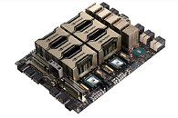
NVIDIA and Global Partners Launch New HGX A100 Systems to Accelerate Industrial AI and HPC

NVIDIA today announced it is turbocharging the NVIDIA HGX AI supercomputing platform with new technologies that fuse AI with high performance computing, making supercomputing more useful to a growing number of industries.

To accelerate the new era of industrial AI and HPC, NVIDIA has added three key technologies to its HGX platform: the NVIDIA A100 80 GB PCIe GPU, NVIDIA NDR 400G InfiniBand networking, and NVIDIA Magnum IO GPUDirect Storage software. Together, they provide the extreme performance to enable industrial HPC innovation.
Return to Keyword Browsing
Apr 29th, 2024 12:54 EDT change timezone

New Forum Posts

Popular Reviews

Controversial News Posts