News Posts matching #HBM2

Return to Keyword Browsing

NVIDIA Details "Pascal" Some More at GTC Japan

NVIDIA revealed more details of its upcoming "Pascal" GPU architecture at the Japanese edition of the Graphics Technology Conference. The architecture will be designed to nearly double performance/Watt over the current "Maxwell" architecture, by implementing the latest tech. This begins with stacked HBM2 (high-bandwidth memory 2). The top "Pascal" based product will feature four 4-gigabyte HBM2 stacks, totaling 16 GB of memory. The combined memory bandwidth for the chip will be 1 TB/s. Internally, bandwidths can touch as high as 2 TB/s. The chip itself will support up to 32 GB of memory, and so enterprise variants (Quadro, Tesla), could max out the capacity. The consumer GeForce variant is expected to serve up 16 GB.

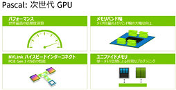
It's also becoming clear that NVIDIA will build its "Pascal" chips on the 16 nanometer FinFET process (AMD will build its next-gen chips on more advanced 14 nm process). NVIDIA is innovating a new interconnect called NVLink, which will change the way the company has been building dual-GPU graphics cards. Currently, dual-GPU cards are essentially two graphics cards on a common PCB, with PCIe bandwidth from the slot shared by a bridge-chip, and an internal SLI bridge connecting the two GPUs. With NVLink, the two GPUs will be interconnected with an 80 GB/s bi-directional data path, letting each GPU directly address memory controlled by the other. This should greatly improve memory management in games that take advantage of newer APIs such as DirectX 12 and Vulkan; and prime the graphics card for higher display resolutions. NVIDIA is expected to launch its first "Pascal" based products in the first half of 2016.

NVIDIA GP100 Silicon Moves to Testing Phase

NVIDIA's next-generation flagship graphics processor, codenamed "GP100," has reportedly graduated to testing phase. That is when a limited batch of completed chips are sent from the foundry partner to NVIDIA for testing and evaluation. The chips tripped speed-traps on changeover airports, on their way to NVIDIA. 3DCenter.org predicts that the GP100, based on the company's "Pascal" GPU architecture, will feature no less than 17 billion transistors, and will be built on the 16 nm FinFET+ node at TSMC. The GP100 will feature an HBM2 memory interface. HBM2 allows you to cram up to 32 GB of memory. The flagship product based on GP100 could feature about 16 GB of memory. NVIDIA's design goal could be to squeeze out anywhere between 60-90% higher performance than the current-generation flagship GTX TITAN-X.

NVIDIA "Pascal" GPUs to be Built on 16 nm TSMC FinFET Node

NVIDIA's next-generation GPUs, based on the company's "Pascal" architecture, will be reportedly built on the 16 nanometer FinFET node at TSMC, and not the previously reported 14 nm FinFET node at Samsung. Talks of foundry partnership between NVIDIA and Samsung didn't succeed, and the GPU maker decided to revert to TSMC. The "Pascal" family of GPUs will see NVIDIA adopt HBM2 (high-bandwidth memory 2), with stacked DRAM chips sitting alongside the GPU die, on a multi-chip module, similar to AMD's pioneering "Fiji" GPU. Rival AMD, on the other hand, could build its next-generation GCNxt GPUs on 14 nm FinFET process being refined by GlobalFoundries.

AMD Details Exascale Heterogenous Processor (EHP) for Supercomputers

AMD published a paper with the IEEE for a new high-density computing device concept, which it calls the Exascale Heterogenous Processor or (EHP). It may be a similar acronym to APU (accelerated processing unit), but is both similar and different to it in many ways, which make it suitable for high-density supercomputing nodes. The EHP is a chip that has quite a bit in common with the recently launched "Fiji" GPU, that drives the company's flagship Radeon R9 Fury X graphics card.

The EHP is a combination of a main die, housing a large number of CPU cores, a large GPGPU unit, and an interposer, which connects the main die to 32 GB of HBM2 memory that's on-package, and is used as both main-memory and memory for the integrated GPGPU unit, without memory partitioning, using hUMA (heterogeneous unified memory access). The CPU component consists of 32 cores likely based on the "Zen" micro-architecture, using eight "Zen" quad-core subunits. There's no word on the CU (compute unit) count of the GPGPU core. The EHP in itself will be highly scalable. AMD hopes to get a working sample of this chip out by 2016-17.

NVIDIA Tapes Out "Pascal" Based GP100 Silicon

Sources tell 3DCenter.org that NVIDIA has successfully taped out its next big silicon based on its upcoming "Pascal" GPU architecture, codenamed GP100. A successor to GM200, this chip will be the precursor to several others based on this architecture. A tape-out means that the company has successfully made a tiny quantity of working prototypes for internal testing and further development. It's usually seen as a major milestone in a product development cycle.

With "Pascal," NVIDIA will pole-vault HBM1, which is making its debut with AMD's "Fiji" silicon; and jump straight to HBM2, which will allow SKU designers to cram up to 32 GB of video memory. 3DCenter.org speculates that GP100 could feature anywhere between 4,500 to 6,000 CUDA cores. The chip will be built on TSMC's upcoming 16 nanometer silicon fab process, which will finally hit the road by 2016. The GP100, and its companion performance-segment silicon, the GP104 (successor to GM204), are expected to launch between Q2 and Q3, 2016.

AMD to Skip 20 nm, Jump Straight to 14 nm with "Arctic Islands" GPU Family

AMD's next-generation GPU family, which it plans to launch some time in 2016, codenamed "Arctic Islands," will see the company skip the 20 nanometer silicon fab process from 28 nm, and jump straight to 14 nm FinFET. Whether the company will stick with TSMC, which is seeing crippling hurdles to implement its 20 nm node for GPU vendors; or hire a new fab, remains to be seen. Intel and Samsung are currently the only fabs with 14 nm nodes that have attained production capacity. Intel is manufacturing its Core "Broadwell" CPUs, while Samsung is manufacturing its Exynos 7 (refresh) SoCs. Intel's joint-venture with Micron Technology, IMFlash, is manufacturing NAND flash chips on 14 nm.

Named after islands in the Arctic circle, and a possible hint at the low TDP of the chips, benefiting from 14 nm, "Arctic Islands" will be led by "Greenland," a large GPU that will implement the company's most advanced stream processor design, and implement HBM2 memory, which offers 57% higher memory bandwidth at just 48% the power consumption of GDDR5. Korean memory manufacturer SK Hynix is ready with its HBM2 chip designs.
Return to Keyword Browsing
Apr 29th, 2024 13:32 EDT change timezone

New Forum Posts

Popular Reviews

Controversial News Posts