News Posts matching #HBM2

Return to Keyword Browsing

Rambus Introduces High Bandwidth Memory PHY on GlobalFoundries FX-14

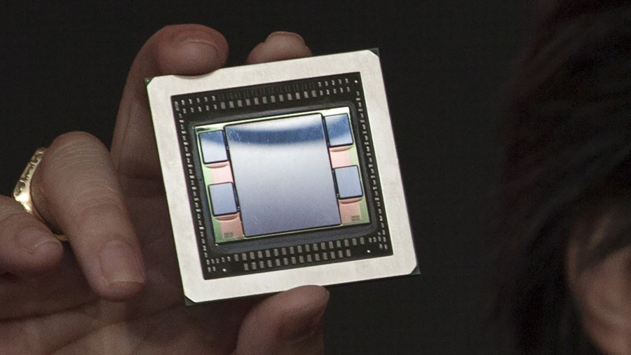
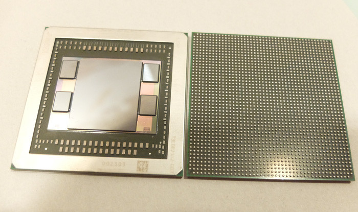
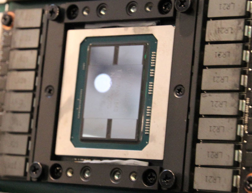
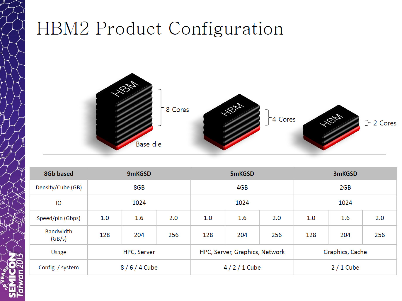
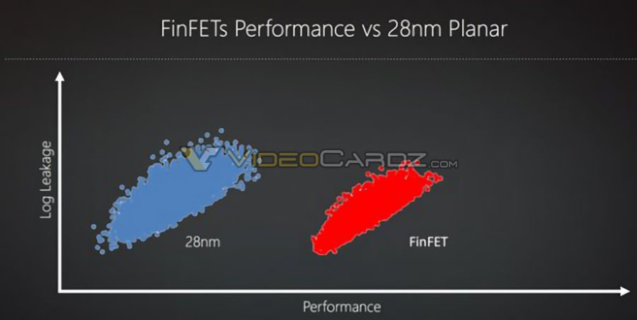
Rambus Inc. today announced the availability of its High Bandwidth Memory (HBM) Gen2 PHY developed for GLOBALFOUNDRIES high-performance FX-14 ASIC Platform. Built on the GLOBALFOUNDRIES 14nm FinFET (14LPP) process technology, the Rambus HBM PHY is aimed at networking and data center applications and designed for systems that require low latency and high bandwidth memory. This PHY is fully compliant with the JEDEC HBM2 standard and supports data rates up to 2000 Mbps per data pin, enabling a total bandwidth of 256 GB/s to meet the needs of today's most data-intensive tasks.

"Data center needs are continuously changing and we are at the forefront of delivering memory interface technology designed to meet today's most demanding workloads," said Luc Seraphin, senior vice president and general manager of the Rambus Memory and Interfaces division. "Through our collaboration with GLOBALFOUNDRIES, we are delivering a comprehensive and robust solution for high-performance data center and networking applications. Our HBM offering will allow data center solution developers to bring high performance memory closer to the CPU, thus reducing latency and improving the system throughput."

AMD VEGA Cube is a Coffee Mug-sized Contraption with 100 TFLOP/s Compute Power

AMD VEGA Cube (working name), is an unannounced product by the company, which could see the light of the day as a Radeon Instinct deep-learning GPGPU solution. This [grande] coffee mug-sized contraption is four GPU subunit boards making up four sides of a cube (well, cuboid), with two sides making up the air channel, likely with space for a compound heatsink or liquid-cooling block, drawing heat from the GPUs lining the inner walls of the cube. The combined compute power of the VEGA Cube, hence, is 100 TFLOP/s (FP16), or 50 TFLOP/s (FP32, single-precision).

Each GPU board is similar in function to NVIDIA's Tesla P100 NVLink board. It has the GPU, VRM, and a high-speed interconnect. The GPUs here in question could be VEGA 10, a multi-chip module with a 25 TFLOP/s (FP16, 12.5 TFLOP/s FP32) GPU die, and 8 GB of HBM2 memory. There are four such GPU boards facing each other. AMD could deploy its much talked about NVLink-alternative, the GMI Coherent Data Fabric, which enables a 100 GB/s data path between neighboring GPUs. It remains to be seen if AMD makes an actual Radeon Instinct product out of this, or of it will remain a really groovy proof of concept.

AMD "Vega" Demoed in Sonoma, California

AMD's next-generation high-end graphics card, based on the "Vega" architecture, was showcased at an event in Sonoma CA, earlier this week. While the architecture is being debuted with the Radeon Instinct MI25 deep-learning accelerator, a prototype graphics card based on the silicon was exhibited by the company, showing Vulkan API gaming.

AMD was pretty tight-lipped about the specifications of this prototype, but two details appear to have slipped out. Apparently, the chip has a floating point performance of 25 TFLOP/s (FP16), and 12.5 TFLOP/s (FP32, single-precision). On paper, this is higher than the 11 TFLOP/s (FP32) of NVIDIA TITAN X Pascal. The other important specification that emerged is that the card features 8 GB of HBM2 memory, with a memory bandwidth of 512 GB/s. This, too, is higher than the 480 GB/s of the TITAN X Pascal. It remains to be seen which market-segment AMD targets with this card.

This article was updated on Dec 15 to accommodate AMD's request to remove all info regarding the demo system, the shown game and its performance, which has been put under NDA retroactively.

AMD Readies Radeon RX 490 for December?

A spectacular rumor doing rounds has AMD sign 2016 off with a new high-end graphics card launch. The company could launch the Radeon RX 490 by the end of the year, according to an Guru3D report. This SKU could either be based on the larger Vega 10 silicon, or be a dual-GPU on a stick graphics card based on a pair of Polaris 10 "Ellesmere" chips. The former seems more likely as multi-GPU support among recent AAA game launches is dwindling. Earlier this year, AMD inadvertently leaked the SKU name Radeon RX 490 on its website.

If the Radeon RX 490 is based on the Vega 10, then it could feature 4,096 stream processors based on the "Vega" architecture, 256 TMUs, 64 ROPs, and a 4096-bit HBM2 memory interface, holding 8 GB or 16 GB of memory, with a memory bandwidth of 512 GB/s. If instead it is a dual-GPU card based on Polaris 10, then you could be looking at 2x 2,304 stream processors, and 16 GB of GDDR5 memory across two 256-bit wide memory interfaces.

AMD Vega 10, Vega 20, and Vega 11 GPUs Detailed

AMD CTO, speaking at an investors event organized by Deutsche Bank, recently announced that the company's next-generation "Vega" GPUs, its first high-end parts in close to two years, will be launched in the first half of 2017. AMD is said to have made significant performance/Watt refinements with Vega, over its current "Polaris" architecture. VideoCardz posted probable specs of three parts based on the architecture.

AMD will begin the "Vega" architecture lineup with the Vega 10, an upper-performance segment part designed to disrupt NVIDIA's high-end lineup, with a performance positioning somewhere between the GP104 and GP102. This chip is expected to be endowed with 4,096 stream processors, with up to 24 TFLOP/s 16-bit (half-precision) floating point performance. It will feature 8-16 GB of HBM2 memory with up to 512 GB/s memory bandwidth. AMD is looking at typical board power (TBP) ratings around 225W.

Vega Not Before 2017: AMD to Investors

In a leaked presentation meant for its investors, AMD states that it expects to launch the "Vega" GPU architecture no sooner than 2017. The company plans to get it out within the first half of 2017. What makes this decision significant is that the company isn't planning on making bigger GPUs on its existing "Polaris" architecture, and its biggest product is the $249 Radeon RX 480. This leaves the company's discrete GPU lineup virtually untended at key price-points above, against NVIDIA's GeForce GTX 1070, GTX 1080, and TITAN X Pascal, at least for the next five months.

In the mean time, AMD could launch additional mobile SKUs based on the Polaris 10 and Polaris 11 chips. The reasons behind this slow-crawl could be many - AMD could be turning its chip-design resources to the various semi-custom SoCs it's working on, for Microsoft and Sony, with their next-generation game consoles; AMD Vega development could also be running in-sync with market availability of HBM2 memory. 2017 promises to be a hectic year for AMD, with launch of not just Vega, but also its "ZEN" CPU architecture, the "Summit Ridge" processor, and APUs based on the CPU micro-architecture.

Third-Generation HBM Could Enable Graphics Cards with 64GB Memory

One of the first drafts of the HBM3 specification reveals that the standard could enable graphics cards with up to 64 GB of video memory. The HBM2 memory, which is yet to make its consumer graphics debut, caps out at 32 GB, and the first-generation HBM, which released with the AMD Radeon Fury series, at just 4 GB.

What's more, HBM3 doubles bandwidth over HBM2, pushing up to 512 GB/s per stack. A 4096-bit HBM3 equipped GPU could have up to 2 TB/s (yes, terabytes per second) of memory bandwidth at its disposal. SK Hynix, one of the key proponents of the HBM standard, even claims that HBM3 will be both more energy-efficient and cost-effective than existing memory standards, for the performance on offer. Some of the first HBM3 implementations could come from the HPC industry, with consumer implementations including game consoles, graphics cards, TVs, etc., following later.

SK Hynix to Ship HBM2 Memory by Q3-2016

Korean memory and NAND flash giant SK Hynix announced that it will have HBM2 memory ready for order within Q3-2016 (July-September). The company will ship 4 gigabyte HBM2 stacks in the 4 Hi-stack (4-die stack) form-factor, in two speeds - 2.00 Gbps (256 GB/s per stack), bearing model number H5VR32ESM4H-20C; and 1.60 Gbps (204 GB/s per stack), bearing model number H5VR32ESM4H-12C. With four such stacks, graphics cards over a 4096-bit HBM2 interface, graphics cards with 16 GB of total memory can be built.

NVIDIA to Unveil GeForce GTX TITAN P at Gamescom

NVIDIA is preparing to launch its flagship graphics card based on the "Pascal" architecture, the so-called GeForce GTX TITAN P, at the 2016 Gamescom, held in Cologne, Germany, between 17-21 August. The card is expected to be based on the GP100 silicon, and could likely come in two variants - 16 GB and 12 GB. The two differ by memory bus width besides memory size. The 16 GB variant could feature four HBM2 stacks over a 4096-bit memory bus; while the 12 GB variant could feature three HBM2 stacks, and a 3072-bit bus. This approach by NVIDIA is identical to the way it carved out Tesla P100-based PCIe accelerators, based on this ASIC. The cards' TDP could be rated between 300-375W, drawing power from two 8-pin PCIe power connectors.

The GP100 and GTX TITAN P isn't the only high-end graphics card lineup targeted at gamers and PC enthusiasts, NVIDIA is also working the GP102 silicon, positioned between the GP104 and the GP100. This chip could lack FP64 CUDA cores found on the GP100 silicon, and feature up to 3,840 CUDA cores of the same kind found on the GP104. The GP102 is also expected to feature simpler 384-bit GDDR5X memory. NVIDIA could base the GTX 1080 Ti on this chip.

Microsoft XBOX Scorpio SoC Powered by "Polaris" and "Zen"

It looks like Microsoft will overpower Sony in the next round of the console wars, with a more powerful SoC on paper. The new XBOX "Scorpio" 4K Ultra HD game console will feature a custom-design SoC by AMD, which will combine not just a GPU based on the "Polaris" architecture, but also a CPU based on the "Zen" microarchitecture. This is significant because it sees a departure from using 8 smaller "Jaguar" CPU cores, and upshifts to stronger "Zen" ones. The chip could be built on the 14 nm process.

The SoC powering the XBOX Scorpio could feature a CPU component with eight "Zen" CPU cores, with SMT enabling 16 logical CPUs, and a "Polaris" GPU with 6 TFLOP/s of compute power. The combined compute power is expected to be close to 10 TFLOP/s. The Radeon RX 480, for instance features 5.84 TFLOP/s of power at its given clock speed. The CPU and GPU will likely share a common memory interface, belting out a memory bandwidth of 320 GB/s. The silicon muscle of this console should power 4K Ultra HD, 1080p @ 60 Hz HDR, and "good VR" solutions such as the Oculus Rift and HTC Vive. Games for the console could leverage DirectX 12.

AMD Pulls Radeon "Vega" Launch to October

In the wake of NVIDIA's GeForce GTX 1080 and GTX 1070 graphics cards, which if live up to their launch marketing, could render AMD's high-end lineup woefully outperformed, AMD reportedly decided to pull the launch of its next big silicon, Vega10, from its scheduled early-2017 launch, to October 2016. Vega10 is a successor to "Grenada," and will be built on the 5th generation Graphics CoreNext architecture (codenamed "Vega").

Vega10 will be a multi-chip module, and feature HBM2 memory. The 14 nm architecture will feature higher performance/Watt than even the upcoming "Polaris" architecture. "Vega10" isn't a successor to "Fiji," though. That honor is reserved for "Vega11." It is speculated that Vega10 will feature 4096 stream processors, and will power graphics cards that compete with the GTX 1080 and GTX 1070. Vega11, on the other hand, is expected to feature 6144 stream processors, and could take on the bigger GP100-based SKUs. Both Vega10 and Vega11 will feature 4096-bit HBM2 memory interfaces, but could differ in standard memory sizes (think 8 GB vs. 16 GB).

AMD's GPU Roadmap for 2016-18 Detailed

AMD finalized the GPU architecture roadmap running between 2016 and 2018. The company first detailed this at its Capsaicin Event in mid-March 2016. It sees the company's upcoming "Polaris" architecture, while making major architectural leaps over the current-generation, such as a 2.5-times performance/Watt uplift and driving the company's first 14 nanometer GPUs; being limited in its high-end graphics space presence. Polaris is rumored to drive graphics for Sony's upcoming 4K Ultra HD PlayStation, and as discrete GPUs, it will feature in only two chips - Polaris 10 "Ellesmere" and Polaris 11 "Baffin."

"Polaris" introduces several new features, such as HVEC (h.265) decode and encode hardware-acceleration, new display output standards such as DisplayPort 1.3 and HDMI 2.0; however, since neither Polaris 10 nor Polaris 11 are really "big" enthusiast chips that succeed the current "Fiji" silicon, will likely make do with current GDDR5/GDDR5X memory standards. That's not to say that Polaris 10 won't disrupt current performance-thru-enthusiast lineups, or even have the chops to take on NVIDIA's GP104. First-generation HBM limits the total memory amount to 4 GB over a 4096-bit path. Enthusiasts will have to wait until early-2017 for the introduction of the big-chip that succeeds "Fiji," which will not only leverage HBM2 to serve up vast amounts of super-fast memory; but also feature a slight architectural uplift. 2018 will see the introduction of its successor, codenamed "Navi," which features an even faster memory interface.

Upcoming AMD "Polaris" and "Vega" GPU Compute Unit Counts Surface

AMD's upcoming GPUs based on the "Polaris" and "Vega" architectures appear to be taking advantage of performance/Watt gains to keep stream processor counts low, and chips small, according to a VideoCardz analysis of curious-looking CompuBench entries. Assuming that a Graphics CoreNext (GCN) compute unit (CU) of the "Polaris" architecture, like the three versions of GCN before it, consists of 64 stream processors, AMD's Polaris 11 silicon, codenamed "Baffin," could feature over 1,024 stream processors, across 16 CUs; Polaris 10, codenamed "Ellesmere," could feature over 2,304 stream processors spread across over 36 CUs; and Vega 10 featuring 4,096 stream processors, spread across 64 CUs.

The "Baffin" silicon succeeds current generation "Curacao" silicon, driving mid-range graphics cards. It is expected to feature a 128-bit wide GDDR5 memory interface, holding 4 GB of memory. The "Ellesmere" silicon succeeds current-generation "Tonga" silicon, driving performance-segment SKUs. It could feature up to 8 GB of GDDR5(X) memory. These two chips could see the light of the day by mid-2016. The third chip out of AMD's stable, Vega 10, could succeed "Fiji," overcoming its biggest marketing shortcoming - 4 GB memory. Taking advantage of HBM2 interface, it could feature 16 GB of memory. It could launch some time in early-2017. AMD is claiming a massive 2.5X performance-per-Watt increase for "Polaris" over the current GCN 1.2 architecture, which drives the "Tonga" and "Fiji" chips, and so these stream processor counts could look deceptively insufficient.

NVIDIA Launches World's First Deep Learning Supercomputer

NVIDIA today unveiled the NVIDIA DGX-1, the world's first deep learning supercomputer to meet the unlimited computing demands of artificial intelligence. The NVIDIA DGX-1 is the first system designed specifically for deep learning -- it comes fully integrated with hardware, deep learning software and development tools for quick, easy deployment. It is a turnkey system that contains a new generation of GPU accelerators, delivering the equivalent throughput of 250 x86 servers.

The DGX-1 deep learning system enables researchers and data scientists to easily harness the power of GPU-accelerated computing to create a new class of intelligent machines that learn, see and perceive the world as humans do. It delivers unprecedented levels of computing power to drive next-generation AI applications, allowing researchers to dramatically reduce the time to train larger, more sophisticated deep neural networks.

Mid-range "Pascal" GPUs Stick to GDDR5-class Memory

At the NVIDIA Drive PX compute module unveiling, company CEO Jen-Hsun Huang gave us the first glimpse of a mid-range GPU based on the "Pascal" architecture. This chip looks a lot more conventional than the fancy HBM2-infused multi-chip module that's at the heart of the Tesla P100. Its package is a traditional green fiberglass substrate with a rectangular die at the center; and is surrounded by conventional-looking GDDR5-class memory chips (which could very well be GDDR5X). The Drive PX is a GPU-accelerated deep-learning box that NVIDIA is basing much of its self-driving car tech around; and uses a pair of these mid-range "Pascal" MXM boards.

NVIDIA Unveils the Tesla P100 HPC Board based on "Pascal" Architecture

NVIDIA unveiled the Tesla P100, the first product based on the company's "Pascal" GPU architecture. At its core is a swanky new multi-chip module, similar in its essential layout to the AMD "Fiji." A 15 billion-transistor GPU die sits on top of a silicon wafer, through which a 4096-bit wide HBM2 memory interface wires it to four 3D HBM2 stacks; and with the wafer sitting on the fiberglass substrate that's rooted into the PCB over a ball-grid array. With the GPU die, wafer, and memory dies put together, this package has a cumulative transistor count of 150 billion transistors. The GPU die is built on the 16 nm FinFET process, and is 600 mm² in area.

The P100 sits on top of a space-efficient PCB that looks less like a video card, and more like a compact module that can be tucked away into ultra-high density supercomputing cluster boxes, such as the new NVIDIA DGX-1. The P100 offers a double-precision (FP64) compute performance of 5.3 TFLOP/s, FP32 performance of 10.6 TFLOP/s, and FP16 performance of a whopping 21.2 TFLOP/s. The chip has registers as big as 14.2 MB, and an L2 cache of 4 MB. In addition to PCI-Express, each P100 chip will be equipped with NVLink, and in-house developed high-bandwidth interconnect by NVIDIA, with bandwidths as high as 80 GB/s per direction, 160 GB/s both directions. This allows extremely high-bandwidth paths between GPUs, so they could share memory and work more like single-GPUs. The P100 is already in volume production, with its target customers already having bought it all the way up to its OEM channel availability some time in Q1-2017.

AMD "Greenland" Vega10 Silicon Features 4096 Stream Processors?

The LinkedIn profile of an R&D manager at AMD discloses key details of the company's upcoming "Greenland" graphics processor, which is also codenamed Vega10. Slated for an early-2017 launch, according to AMD's GPU architecture roadmap, "Greenland" will be built on AMD's "Vega" GPU architecture, which succeeds even the "Polaris" architecture, which is slated for later this year.

The LinkedIn profile of Yu Zheng, an R&D manager at AMD (now redacted), screencaptured by 3DCenter.org, reveals the "shader processor" (stream processor) count of Vega10 to be 4,096. This may look identical to the SP count of "Fiji," but one must take into account "Greenland" being two generations of Graphics CoreNext tech ahead of "Fiji," and that the roadmap slide hints at HBM2 memory, which could be faster. One must take into account AMD's claims of a 2.5X leap in performance-per-Watt over the current architecture with Polaris, so Vega could only be even faster.

NVIDIA's Next Flagship Graphics Cards will be the GeForce X80 Series

With the GeForce GTX 900 series, NVIDIA has exhausted its GeForce GTX nomenclature, according to a sensational scoop from the rumor mill. Instead of going with the GTX 1000 series that has one digit too many, the company is turning the page on the GeForce GTX brand altogether. The company's next-generation high-end graphics card series will be the GeForce X80 series. Based on the performance-segment "GP104" and high-end "GP100" chips, the GeForce X80 series will consist of the performance-segment GeForce X80, the high-end GeForce X80 Ti, and the enthusiast-segment GeForce X80 TITAN.

Based on the "Pascal" architecture, the GP104 silicon is expected to feature as many as 4,096 CUDA cores. It will also feature 256 TMUs, 128 ROPs, and a GDDR5X memory interface, with 384 GB/s memory bandwidth. 6 GB could be the standard memory amount. Its texture- and pixel-fillrates are rated to be 33% higher than those of the GM200-based GeForce GTX TITAN X. The GP104 chip will be built on the 16 nm FinFET process. The TDP of this chip is rated at 175W.

AMD Unveils GPU Architecture Roadmap, "Polaris" to Skip HBM2 Memory?

Alongside its big Radeon Pro Duo flagship graphics card launch, AMD unveiled its GPU architecture roadmap that looks as far into the future as early-2018. By then, AMD will have launched as many as three new GPU architectures. It begins with the launch of its 4th generation Graphics CoreNext architecture, codenamed "Polaris," in mid-2016. Built on the 14 nm FinFET process, "Polaris" is expected to offer a whopping 2.5x increase in performance-per-Watt for AMD, compared to its current GCN 1.2 architecture on 28 nm.

Hot on Polaris' heels, in early-2017, AMD plans to launch the "Vega" GPU architecture. While this appears to offer a 50% increase in performance-per-Watt over Polaris, its highlight is HBM2 memory. Does this mean that AMD plans to skip HBM2 on Polaris, and stick to GDDR5X? Could AMD be opting for a similar approach to NVIDIA, by launching its performance-segment GPU first as an enthusiast product, giving it a free run on the markets till early-2017, and then launching a Vega-based big-chip with HBM2 memory, taking over as the enthusiast-segment product? Some time in early-2018, AMD will launch the "Navi" architecture, which appears to offer a 2.5x performance-per-Watt lead over Polaris, taking advantage of an even newer memory standard.

NVIDIA "GP104" Silicon to Feature GDDR5X Memory Interface

It looks like NVIDIA's next GPU architecture launch will play out much like its previous two generations - launching the second biggest chip first, as a well-priced "enthusiast" SKU that outperforms the previous-generation enthusiast product, and launching the biggest chip later, as the high-end enthusiast product. The second-biggest chip based on NVIDIA's upcoming "Pascal" architecture, the "GP104," which could let NVIDIA win crucial $550 and $350 price-points, will be a lean machine. NVIDIA will design the chip to keep manufacturing costs low enough to score big in price-performance, and a potential price-war with AMD.

As part of its efforts to keep GP104 as cost-effective as possible, NVIDIA could give exotic new tech such as HBM2 memory a skip, and go with GDDR5X. Implementing GDDR5X could be straightforward and cost-effective for NVIDIA, given that it's implemented the nearly-identical GDDR5 standard on three previous generations. The new standard will double densities, and one could expect NVIDIA to build its GP104-based products with 8 GB of standard memory amounts. GDDR5X breathed a new lease of life to GDDR5, which had seen its clock speeds plateau around 7 Gbps/pin. The new standard could come in speeds of up to 10 Gbps at first, and eventually 12 Gbps and 14 Gbps. NVIDIA could reserve HBM2 for its biggest "Pascal" chip, on which it could launch its next TITAN product.

SK Hynix to Ship 4GB HBM2 Stacks by Q3-2016

Korean DRAM and NAND flash giant SK Hynix will be ready to ship its 4 GB stacked second generation high-bandwidth memory (HBM2) chips from Q3, 2016. These packages will be made up of four 1 GB dies, with a bandwidth-per-pin of 1 Gbps, 1.6 Gbps, and 2 Gbps, working out to per-stack bandwidths of 128 GB/s, 204 GB/s, and 256 GB/s, respectively.

These chips will target applications such as graphics cards, network infrastructure, HPC, and servers. The company is also designing 8 GB stacks, made up of eight 1 GB dies. These stacks will be targeted at HPC and server applications. The company is also offering cost-effective 2 GB, 2-die stacks, for graphics cards. The cost-effective 2 GB, 2-die stacks could prove particularly important for the standard's competition against GDDR5X, particularly in mid-range and performance-segment graphics cards.

NVIDIA GP100 Silicon to Feature 4 TFLOPs DPFP Performance

NVIDIA's upcoming flagship GPU based on its next-generation "Pascal" architecture, codenamed GP100, is shaping up to be a number-crunching monster. According to a leaked slide by an NVIDIA research fellow, the company is designing the chip to serve up double-precision floating-point (DPFP) performance as high as 4 TFLOP/s, a 3-fold increase from the 1.31 TFLOP/s offered by the Tesla K20, based on the "Kepler" GK110 silicon.

The same slide also reveals single-precision floating-point (SPFP) performance to be as high as 12 TFLOP/s, four times that of the GK110, and nearly double that of the GM200. The slide also appears to settle the speculation on whether GP100 will use stacked HBM2 memory, or GDDR5X. Given the 1 TB/s memory bandwidth mentioned on the slide, we're inclined to hand it to stacked HBM2.

Samsung Begins Mass-Producing 4-Gigabyte HBM2 Memory Stacks

Samsung Electronics Co., Ltd., announced today that it has begun mass producing the industry's first 4-gigabyte (GB) DRAM package based on the second-generation High Bandwidth Memory (HBM2) interface, for use in high performance computing (HPC), advanced graphics and network systems, as well as enterprise servers. Samsung's new HBM solution will offer unprecedented DRAM performance - more than seven times faster than the current DRAM performance limit, allowing faster responsiveness for high-end computing tasks including parallel computing, graphics rendering and machine learning.

"By mass producing next-generation HBM2 DRAM, we can contribute much more to the rapid adoption of next-generation HPC systems by global IT companies," said Sewon Chun, senior vice president, Memory Marketing, Samsung Electronics. "Also, in using our 3D memory technology here, we can more proactively cope with the multifaceted needs of global IT, while at the same time strengthening the foundation for future growth of the DRAM market."

The newly introduced 4GB HBM2 DRAM, which uses Samsung's most efficient 20-nanometer process technology and advanced HBM chip design, satisfies the need for high performance, energy efficiency, reliability and small dimensions making it well suited for next-generation HPC systems and graphics cards.

4th Generation Graphics CoreNext Architecture Codenamed "Polaris"

The fourth generation of AMD Graphics CoreNext GPU architecture has been reportedly codenamed "Polaris" by the company. It makes its debut later this year in the company's "Arctic Islands" GPUs, built on Samsung's 14 nm FinFET node. According to the company, Polaris will provide a "historic leap in performance/Watt" for Radeon GPUs. Chips based on Polaris will feature improvements to not just the compute units, but will also come with generational improvements to pretty much every other component, including a new front-end, display controllers, and a new memory controller supporting HBM2.

AMD debuted its first generation GCN architecture with the Radeon HD 7000 series, notably the "Tahiti" silicon. Its second-generation, GCN 2.0, (reported in the press as GCN 1.1), debuted with the R9 290 series, notably the "Hawaii" silicon. The third-generation, GCN 3.0 (reported in the press as GCN 1.2), debuted with the R9 285, notably the "Tonga" silicon; making "Polaris" the fourth-generation. GCN 4.0 will form the core micro-architecture of the "Arctic Islands" family of GPUs, which make their debut in mid-2016.
Return to Keyword Browsing
Apr 26th, 2024 19:07 EDT change timezone

New Forum Posts

Popular Reviews

Controversial News Posts