News Posts matching #HBM2

Return to Keyword Browsing

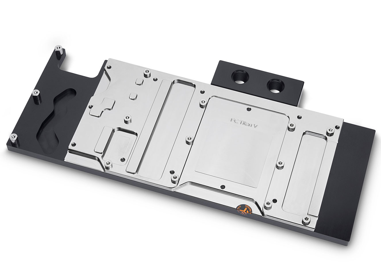
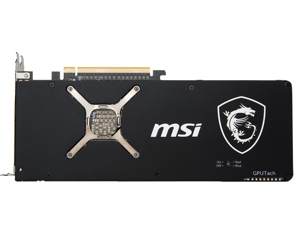
AMD 7nm "Vega" by December, Not a Die-shrink of "Vega 10"

AMD is reportedly prioritizing its first 7 nanometer silicon fabrication allocations to two chips - "Rome," and "Vega 20." Rome, as you'll recall, is the first CPU die based on the company's "Zen 2" architecture, which will build the company's 2nd generation EPYC enterprise processors. "Vega 20," on the other hand, could be the world's first 7 nm GPU.

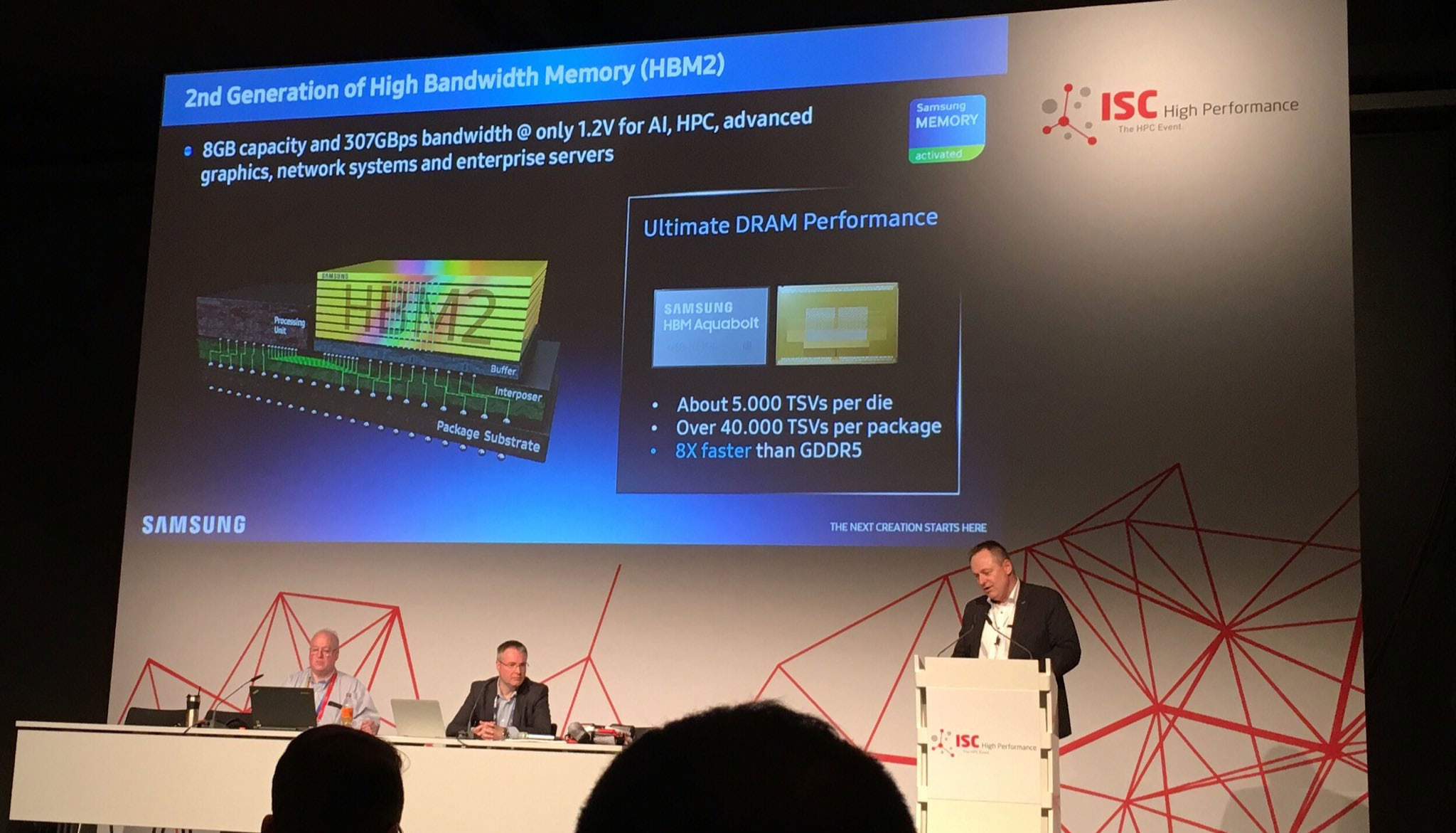
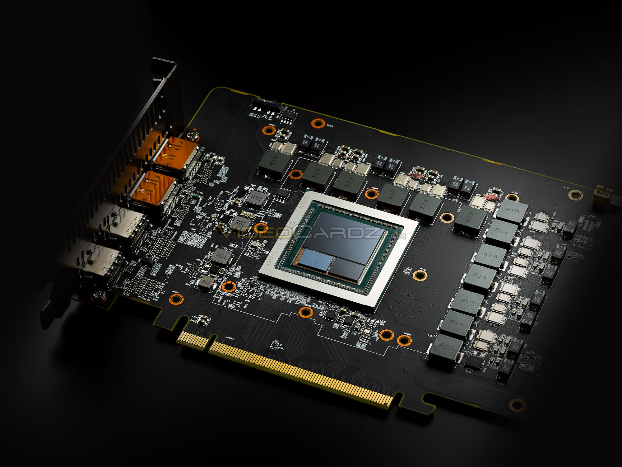
"Vega 20" is not a mere die-shrink of the "Vega 10" GPU die to the 7 nm node. For starters, it is flanked by four HBM2 memory stacks, confirming it will feature a wider memory interface, and support for up to 32 GB of memory. AMD at its Computex event confirmed that "Vega 20" will build Radeon Instinct and Radeon Pro graphics cards, and that it has no plans to bring it to the client-segment. That distinction will be reserved for "Navi," which could only debut in 2019, if not later.

AMD Radeon Pro WX 8200 Detailed

AMD is giving final touches to the new Radeon Pro WX 8200 professional graphics card. Launched over a year following the Radeon Pro WX 9100, the WX 8200 has a leaner feature-set, while continuing to be based on AMD's current IP. The card still uses the 14 nm "Vega 10" MCM, but with a core-config akin to that of the RX Vega 56. You get 56 NGCUs working out to 3,584 stream processors, 224 TMUs, 64 ROPs, and a 4096-bit wide HBM2 memory interface, handling 16 GB of memory on this card. The air-cooled card also has a leaner connectivity load-out, with just four mini-DisplayPort 1.4 connectors (the WX 9100 comes with six). Its 8-pin + 6-pin connectors are positioned at the rear-end to be SSI workstation-friendly. The card surfaced on CompuBench database, in which its performance numbers are only slightly behind those of the WX 9100, but significantly better than the "Polaris 20" based WX 7100. AMD is expected to launch this card at SIGGRAPH 2018.

AMD Vega 20 GPU Could Implement PCI-Express gen 4.0

The "Vega 20" silicon will be significantly different from the "Vega 10" which powers the company's current Radeon RX Vega series. AMD CEO Dr. Lisa Su unveiled the "Vega 20" silicon at the company's 2018 Computex event, revealing that the multi-chip module's 7 nm GPU die is surrounded by not two, but four HBM2 memory stacks, making up to 32 GB of memory. Another key specification is emerging thanks to the sharp eyes at ComputerBase.de - system bus.

A close inspection of the latest AMDGPU Linux driver includes PCI-Express link speed definitions for PCI-Express gen 4.0, which offers 256 Gbps of bandwidth per direction at x16 bus width, double that of PCI-Express gen 3.0. "Vega 20" got its first PCIe gen 4.0 support confirmation from a leak slide that surfaced around CES 2018. AMD "Vega" architecture slides from last year hinted at a Q3/Q4 launch of the first "Vega 20" based product. The same slide also hinted that the next-generation EPYC processor, which we know are "Zen 2" based and not "Zen+," could feature PCI-Express gen 4.0 root-complexes. Since EPYC chips are multi-chip modules, it could also hint at the likelihood of PCIe gen 4.0 on "Zen 2" based 3rd generation Ryzen processor family.

Samsung Doubles its HBM2 Output, May Still Fall Short of Demand

Samsung has reportedly doubled its manufacturing output of HBM2 (high-bandwidth memory 2) stacks. Despite this, the company may still fall short of the demand for HBM2, according to HPC expert Glenn K Lockwood, Tweeting from the ISC 2018, the annual HPC industry event held between 24th to 28th June in Frankfurt, where Samsung was talking about its 2nd generation "Aquabolt" HBM2 memory, which is up to 8 times faster than GDDR5, with up to 307 GB/s bandwidth from a single stack.

While HBM2 is uncommon on consumer graphics cards (barring AMD's flagship Radeon RX Vega series, and NVIDIA's TITAN V), the memory type is in high demand with HPC accelerators that are mostly GPU-based, such as AMD Radeon Instinct series, and NVIDIA Tesla. The HPC industry itself is riding the gold-rush of AI research based on deep-learning and neural-nets. FPGAs, chips that you can purpose-build for your applications, are the other class of devices soaking up HBM2 inventories. The result of high demand, coupled with high DRAM prices could mean HBM2 could still be too expensive for mainstream client applications.

AMD Radeon Vega 12 and Vega 20 Listed in Ashes Of The Singularity Database

Back at Computex, AMD showed a demo of their Vega 20 graphics processor, which is produced using a refined 7 nanometer process. We also reported that the chip has a twice-as-wide memory interface, effectively doubling memory bandwidth, and alsomaximum memory capacity. The smaller process promises improvements to power efficiency, which could let AMD run the chip at higher frequencies for more performance compared to the 14 nanometer process of existing Vega.

As indicated by AMD during Computex, the 7 nanometer Vega is a product targeted at High Performance Compute (HPC) applications, with no plans to release it for gaming. As they clarified later, the promise of "7 nanometer for gamers" is for Navi, which follows the Vega architecture. It's even more surprising to see AOTS results for a non-gaming card - my guess is that someone was curious how well it would do in gaming.

AMD "Vega 20" Optical-Shrunk GPU Surfaces in Linux Patches

AMD "Vega 20" is rumored to be an optical shrink of the current "Vega 10" GPU die to a newer process, either 12 nm, or 10 nm, or perhaps even 7 nm. Six new device IDs that point to "Vega 20" based products, surfaced on AMD's GPU drivers source code, with its latest commit made as recently as on 28th March. AMD "Vega 10" is a multi-chip module of a 14 nm GPU die, and two "10 nm-class" HBM2 memory stacks, sitting on a silicon interposer that facilitates high-density wiring between the three. In an effort to increase clock speeds, efficiency, or both, AMD could optically shrink the GPU die to a smaller silicon fabrication process, and carve out a new product line based on the resulting chip.

EK Releases Full-coverage Water Block for ASUS ROG Strix RX Vega Series

EK Water Blocks, the Slovenia-based premium computer liquid cooling gear manufacturer, is releasing EK-FC Radeon Vega Strix water blocks that are compatible with the ASUS ROG Strix RX VEGA64. This kind of efficient cooling will allow your high-end graphics card to reach higher boost clocks, thus providing more performance during gaming or other GPU intense tasks.

This water block directly cools the GPU, HBM2 memory, and VRM (voltage regulation module) as water flows directly over these critical areas thus allowing the graphics card and it's VRM to remain stable under high overclocks. EK-FC Radeon Vega Strix water block features a central inlet split-flow cooling engine design for best possible cooling performance, which also works flawlessly with reversed water flow without adversely affecting the cooling performance. This kind of efficient cooling will allow your high-end graphics card to reach higher boost clocks, thus providing more performance during gaming or other GPU intense tasks. Moreover, such design offers great hydraulic performance allowing this product to be used in liquid cooling systems using weaker water pumps.

Intel "Hades Canyon" NUC Armed with Vega M Plays Anything at 1080p

Intel's upcoming "Hades Canyon" NUC, the spiritual successor to the company's "Skull Canyon" NUC; will be one of the first commercial implementations of the "Kaby Lake-G" multi-chip module, which puts an AMD Radeon Vega M graphics part and a quad-core "Kaby Lake" die together on a package, along with 4 GB of HBM2 memory for the GPU, when they start shipping in Spring 2018, priced between $799-$999. Korean tech publication Playwares got its hands on one of these, and its testing suggests that it achieves the key design goal of Kaby Lake-G: to be able to play any of today's games at 1080p (with acceptable levels of eye-candy.)

Playwares put "Hades Canyon" through three of today's AAA game titles that take advantage of DirectX 12: "Rise of the Tomb Raider," "Tom Clancy's The Division," and "Total War: Warhammer 2." At default clocks, and 1080p resolution, "Rise of the Tomb Raider" puts out around 53 fps, with 45.36 fps (minimum, 99th percentile). When overclocked, the chip averages 59.11 fps, with 50.5 fps (minimum, 99th percentile). "The Division" averages 41.5 fps at default clocks, and 46.8 fps when overclocked. "Warhammer 2" is a lot more taxing on the chip - 27.3 fps average and 23 fps minimum at default clocks, and 30.1 average with 26 fps minimum, when overclocked. One has to take into account that the "Vega M" chip on the Core i7-8709G is significantly more powerful than the iGPU of AMD's Ryzen "Raven Ridge" APUs - 1536 stream processors, 96 TMUs, 32 ROPs, and 1024-bit HBM2 memory; versus 704 stream processors, 44 TMUs, 16 ROPs, and system memory share.

EK Unveils NVIDIA TITAN V Full-coverage Water-block

EK Water Blocks, the Slovenia-based premium computer liquid cooling gear manufacturer, is releasing water blocks for the most powerful PC GPU on the market to this day, the NVIDIA Titan V. The EK-FC Titan V full cover GPU water block will help you enjoy the full computing power of the Volta architecture based NVIDIA Titan V in a silent environment.

This water block directly cools the GPU, HBM2 memory, and VRM (voltage regulation module) as well! Water is channeled directly over these critical areas, thus allowing the graphics card and it's VRM to remain stable under high overclocks and to reach full boost clocks. EK-FC Titan V water block features a central inlet split-flow cooling engine design for best possible cooling performance, which also works flawlessly with reversed water flow without adversely affecting the cooling performance. Moreover, such design offers great hydraulic performance allowing this product to be used in liquid cooling systems using weaker water pumps.

Sapphire Launches Pulse Radeon RX Vega 56 Graphics Card

Sapphire over the weekend officially launched its cost-effective custom-design Radeon RX Vega 56 graphics card, the Pulse Radeon Vega 56 (model: 11276-02), which began appearing on European e-tailers late-January. The card combines a custom-design short-length PCB that's roughly the length of AMD's reference R9 Fury board; with a beefy custom-design cooling solution that features two large aluminium fin-stacks, ventilated by a pair of 100 mm double ball-bearing fans.

The card offers out of the box clock speeds of 1208 MHz core, 1512 MHz boost, and 800 MHz (1.60 GHz HBM2 effective) memory, against AMD reference clock speeds of 1138 MHz core and 1474 MHz boost. At its given clock, the memory bandwidth on offer is 409.6 GB/s. The "Vega 10" silicon is configured with 3,584 stream processors, 192 TMUs, and 64 ROPs. The card draws power from a pair of 8-pin PCIe power connectors, display outputs include three DisplayPort 1.4 and one HDMI 2.0. Sapphire intended for this SKU to ideally occupy a close-to-reference price-point, a notch below its Nitro+ series, however in the wake of the crypto-currency wave, market-forces will decide its retail price.

Intel Core i7-8705G with Vega M Obliterates 8th Gen Core + GeForce MX 150

It looks like Intel has achieved the design goals of its new Core i7-8705G multi-chip module, built in collaboration with AMD. Combining a 4-core/8-thread "Kaby Lake" CPU die with an AMD "Vega" GPU die that has its own 4 GB HBM2 memory stack, the ruthless duo put similarly-priced discrete GPU setups to rest, such as the combination of an 8th generation Core processor + NVIDIA GeForce MX 150. More importantly, entry-level discrete GPU combinations with high-end mobile CPUs have a similar power/thermal envelope as the i7-8705G MCM, but at significantly higher PCB footprint.

Dell implemented the Core i7-8705G on one of its latest XPS 15 2-in-1 models. The device was compared to an Acer Swift 3 (SF314-51), which combines a Core i5-8250U processor with GeForce MX 150 discrete graphics; and a Dell XPS 13 9370, which implements an 8th generation Core processor that has Intel's workhorse graphics core, the HD 620. The three devices squared off against each other at "Rise of the Tomb Raider" game benchmark. The i7-8705G averaged 35 frames per second (fps), while the MX 150 barely managed 24 fps. The HD 620 ran a bored intern's PowerPoint slideshow at 9 fps.

Intel Could Ditch AMD dGPU Die on Future Core G-series MCMs with "Arctic Sound"

Intel did the impossible in 2017, by collaborating with rival AMD after decades, on a product. The new Core i7-8000G series processors are multi-chip modules that combine quad-core "Kaby Lake" CPU dies with discrete AMD Radeon Vega GPU dies that have their own dedicated HBM2 stacks. With performance-segment notebooks and sleek AIO desktops building momentum for such products, Intel sees a future in building its own discrete GPUs, at least dies that can replace the AMD Radeon IP from its Core G-series processors.

With former AMD Graphics head Raja Koduri switching to Intel amidst rumors of the company investing in discrete GPUs of its own, details emerge of the company's future "Arctic Sound" and "Jupiter Sound" graphics IP, which point to the possibility of them being discrete GPU dies based on the Gen 12 and Gen 13 graphics architectures, respectively. According to Ashraf Eassa, a technology stock commentator with "The Motley Fool," both "Arctic Sound" and "Jupiter Sound" are discrete GPU dies that connect with Intel processor dies over EMIB, the company's proprietary high-density interconnect for multi-chip modules. It could be a long wait leading up to the two, since the company is still monetizing its Gen 9.5 architecture on 8th generation Core processors.

Samsung Starts Mass-producing 2.4 Gbps 8GB HBM2 Stacks

Samsung Electronics Co., Ltd., the world leader in advanced memory technology, today announced that it has started mass production of its 2nd-generation 8-gigabyte (GB) High Bandwidth Memory-2 (HBM2) with the fastest data transmission speed on the market today. The new solution, Aquabolt, which is the industry's first HBM2 to deliver a 2.4 gigabits-per-second (Gbps) data transfer speed per pin, should accelerate the expansion of supercomputing and the graphics card market.

"With our production of the first 2.4 Gbps 8 GB HBM2, we are further strengthening our technology leadership and market competitiveness," said Jaesoo Han, executive vice president, Memory Sales & Marketing team at Samsung Electronics. "We will continue to reinforce our command of the DRAM market by assuring a stable supply of HBM2 worldwide, in accordance with the timing of anticipated next-generation system launches by our customers."

NVIDIA Quadro GV100 Surfaces in Latest NVFlash Binary

NVIDIA could be giving final touches to its Quadro GV100 "Volta" professional graphics card, after the surprise late-2017 launch of the NVIDIA TITAN V. The card was found listed in the binary view of the latest version of NVFlash (v5.427.0), the most popular NVIDIA graphics card BIOS extraction and flashing utility. Since its feature-set upgrade to the TITAN Xp through newer drivers, NVIDIA has given the TITAN family of graphics cards a quasi-professional differentiation from its GeForce GTX family.

The Quadro family still has the most professional features, software certifications, and are sought after by big companies into graphics design, media, animation, architecture, resource exploration, etc. The Quadro GV100 could hence yet be more feature-rich than the TITAN V. With its GV100 silicon, NVIDIA is using a common ASIC and board design for its Tesla V100 PCIe add-in card variants, the TITAN V, and the Quadro GV100. While the company endowed the TITAN V with 12 GB of HBM2 memory using 3 out of 4 memory stacks the ASIC is capable of holding; there's an opportunity for NVIDIA to differentiate the Quadro GV100 by giving it that 4th memory stack, and 16 GB of total memory. You can download the latest version of NVFlash here.

Intel Core i7-8709G with Vega M Graphics Parsed by Futuremark SystemInfo

Ahead of its Q1-2018 launch after a CES reveal, Intel's Core i7-8709G multi-chip module (MCM) was picked up by Thai PC enthusiast and tech vlogger "TUM APISAK," revealing some of its first specifications as read by Futuremark SystemInfo, a hardware-detection component common to various Futuremark benchmark suites. The "Kaby Lake-G" MCM combines a quad-core "Kaby Lake" CPU die with an AMD Radeon "Vega M" graphics die that has a dedicated HBM2 memory stack on-package.

Futuremark SystemInfo puts out quite a few specs of the i7-8709G, beginning with its 4-core/8-thread CPU based on the "Kaby Lake" micro-architecture, which is clocked at 3.10 GHz with 3.90 GHz Turbo Boost; Radeon RX Vega M (694C:C0) graphics core with 4 GB of HBM2 memory across a 1024-bit memory bus; with its GPU engine running at 1.19 GHz, and memory at 800 MHz (204.8 GB/s memory bandwidth); although the core-config of the iGPU remains a mystery. We recommend you maximize the video below for legible details.

Intel Unveils Industry's First FPGA Integrated with HBM - Built for Acceleration

Intel today announced the availability of the Intel Stratix 10 MX FPGA, the industry's first field programmable gate array (FPGA) with integrated High Bandwidth Memory DRAM (HBM2). By integrating the FPGA and the HBM2, Intel Stratix 10 MX FPGAs offer up to 10 times the memory bandwidth when compared with standalone DDR memory solutions1. These bandwidth capabilities make Intel Stratix 10 MX FPGAs the essential multi-function accelerators for high-performance computing (HPC), data centers, network functions virtualization (NFV), and broadcast applications that require hardware accelerators to speed-up mass data movements and stream data pipeline frameworks.

In HPC environments, the ability to compress and decompress data before or after mass data movements is paramount. HBM2-based FPGAs can compress and accelerate larger data movements compared with stand-alone FPGAs. With High Performance Data Analytics (HPDA) environments, streaming data pipeline frameworks like Apache Kafka and Apache Spark Streaming require real-time hardware acceleration. Intel Stratix 10 MX FPGAs can simultaneously read/write data and encrypt/decrypt data in real-time without burdening the host CPU resources.

MSI Intros Radeon RX Vega 56 Air Boost Graphics Cards

MSI rolled out the Radeon RX Vega 56 Air Boost and Air Boost OC graphics cards. The two are based on the same board design as the RX Vega 64 Air Boost series the company launched last week. The quasi-custom design card combines an AMD reference-design PCB with a custom-design lateral-flow cooler by MSI that's similar in design to AMD's cost-effective reference cooler. Adding to its effectiveness is the heavily perforated rear I/O bracket.

The base model sticks to AMD reference clock speeds of 1156 MHz core and 1471 MHz boost; while the OC variant ships with 1181 MHz core and 1520 MHz boost. Both cards leave the HBM2 memory clock untouched at 800 MHz. The cards draw power from a pair of 8-pin PCIe power connectors; display outputs include an HDMI 2.0, and three DisplayPort 1.4 connectors. The base variant sells at USD $399, with the OC variant going for $439.

NVIDIA Titan V Achieves 82 MH/s in Ethereum Mining

"But how well does it mine?" This is one of the questions in the mind of many in the enthusiast community whenever a new GPU is launched. These are a fickle lot, to be sure; their primary interest is the power/performance ratio of any graphics card, which enables miners to maximize profits. Price/performance isn't much of a concern when users are confident they'll recoup the totality of their investment in the medium run - and sometimes even the short run, if recent changes in Ethereum pricing are any indication.

The folks at HotHardware have put an NVIDIA Titan V through its paces in Ethereum mining, eager to see this Volta-based chips' prowess in this type of workloads. Titan V reveals itself as a graphics card that achieves 69 MH/s at stock settings - and an even more impressive 82 MH/s when slightly overclocked. Overclocking methodology was simple - increase temperature and power targets for the Titan V, and then increase memory frequency until a bottleneck was found. And voila. The Titan V was happily churning out 82 MH/s in version 10.2 of the Claymore Miner - more than double the output of an RX Vega 64 and Titan Xp. Power consumption wasn't detailed in this test, and the Titan V would almost definitely consume more power than a Titan Xp - the chip is double the size - but when we take into account the fact that its TDP is the same, that it's built on a 12 nm process against the Titan Xp's 16 nm, and that it uses HBM2 memory instead of GDDR5X... Well, the differences likely aren't anything to write home about. But the performance is. I'll leave it over to our expert miners to say whether they'd invest in a Titan V for mining - all $2,999 of it.

Rambus Talks HBM3, DDR5 in Investor Meeting

Rambus, a company that has veered around the line of being an innovative company and a patent troll, has shed some more light on what can be expected from HBM3 memory (when it's finally available). In an investor meeting, representatives from the company shared details regarding HBM3's improvements over HBM2. Details are still scarce, but at least we know Rambus' expectations for the technology: double the memory bandwidth per stack when compared to HBM2 (4000 MB/s), and a more complex design, which leaves behind the 2.5D design due to increased height of the HBM3 memory stacks. An interesting thing to note is that Rambus is counting on HBM3 to be produced on 7 nm technologies. Considering the overall semiconductor manufacturing calendar for the 7 nm process, this should place HBM3 production in 2019, at the earliest.

HBM3 is also expected to bring much lower power consumption compared to HBM2, besides increasing memory density and bandwidth. However, the "complex design architectures" in the Rambus slides should give readers pause. HBM2 production has had some apparent troubles in reaching demand levels, with suspected lower yields than expected being the most likely culprit. Knowing the trouble AMD has had in successful packaging of HBM2 memory with the silicon interposer and its own GPUs, an even more complex implementation of HBM memory in HBM3 could likely signal some more troubles in that area - maybe not just for AMD, but for any other takers of the technology. Here's hoping AMD's woes were due only to one-off snags on their packaging partners' side, and doesn't spell trouble for HBM's implementation itself.

PowerColor Officially Launches Radeon RX Vega Red Devil Series

TUL Corporation, a leading and innovative manufacturer of AMD graphic cards since 1997, has launched a new PowerColor Red Devil RX VEGA 64 and Red Devil RX VEGA 56 and opened up a new generation of the graphics cards market. The VEGA series are for the extreme gamers looking for the highest resolutions, highest framerates in maximum video setting.

The PowerColor RX VEGA graphics are designed to deliver exhilarating performance in the latest DirectX 12 and Vulkan game titles. With a dedicated High-Bandwidth Cache, the VEGA utilizes HBM2, the latest in graphic memory technology, to provide incredible levels of power efficiency and memory performance. The Next-Gen Pixel Engine found in the Vega GPU is designed to boost shading performance more efficiently to bring the latest VR and extreme resolution games to life.

EK Water Blocks Announces Availability of the EK-MLC Phoenix

EK-MLC Phoenix is a Modular Liquid Cooling line of products and the next generation of improved All-In-One water cooling solutions. It is a new lineup of pre-filled products for liquid cooling, the 2nd generation of improved EK All-In-One products. Created for the market segment of customers who are unwilling to assemble a full custom loop or don't have enough time for maintenance of their PCs, but still insist on a high-end cooling solution. The most important feature of EK-MLC is the modular design and the ability to add multiple pre-filled water blocks in any order.

Modular Liquid Cooling line of products is designed around Quick Disconnect Couplings and it brings a modular approach to connecting and expanding the loop, giving you the freedom to decide which components you want to cool down. CPU cooling module and GPU cooling module can be connected to the radiator core module in any order, separately or together.

PowerColor Radeon RX Vega 64 Red Devil Available Soon, Overclocked, £590

It seems our wait for custom editions of AMD's RX Vega graphics cards is coming to an end. "Better late than never" is what they always say; however, AMD and its AIB partners have to know that this kind of wait can sap customer enthusiasm for a product. It's not enough that customers waited around two years for Vega to come to fruition; we've also had to wait some additional months (not weeks), for an actual custom-design graphics card. Vega's exotic design with HBM2 memory means that these graphics cards' availability would fall prey not only to Vega GPU yields, but also to HBM2 memory availability.

Additionally, Vega has been vulnerable to packaging of HBM2 and the GPU as well, with various factories providing different levels of quality in the finished product. This introduced some unexpected variance in the finished products - making the creation of cooling designs that could cope with all the design discrepancies more difficult.

Intel Announces "Coffee Lake" + AMD "Vega" Multi-chip Modules

Rumors of the unthinkable silicon collaboration between Intel and AMD are true, as Intel announced its first multi-chip module (MCM), which combines a 14 nm Core "Coffee Lake-H" CPU die, with a specialized 14 nm GPU die by AMD, based on the "Vega" architecture. This GPU die has its own HBM2 memory stack over a 1024-bit wide memory bus. Unlike on the AMD "Vega 10" and "Fiji" MCMs, in which a silicon interposer is used to connect the GPU die to the memory stacks, Intel deployed the Embedded Multi-Die Interconnect Bridge (EMIB), a high-density substrate-level wiring. The CPU and GPU dies talk to each other over PCI-Express gen 3.0, wired through the package substrate.

This multi-chip module, with a tiny Z-height, significantly reduces the board footprint of the CPU + discrete graphics implementation, when compared to having separate CPU and GPU packages with the GPU having discrete GDDR memory chips, and enables a new breed of ultra portable notebooks that pack a solid graphics muscle. The MCM should enable devices as thin as 11 mm. The specifications of the CPU and dGPU dies remain under the wraps. The first devices with these MCMs will launch by Q1 2018.
A video presentation follows.

AMD to Build 2nd Gen. Ryzen and Radeon Vega on GloFo 12nm

Not to be held back by silicon fabrication process limitations like in the past, AMD will build its second-generation Ryzen CPUs and Radeon Vega GPUs on the new 12 nanometer LP (low power) FinFET process by GlobalFoundries. From the looks of it, "2nd generation Ryzen" doesn't seem to be the same as "Zen2" (a micro-architectural advancement due to be built on the 7 nm process), and is more likely an optical shrink of existing 14 nm IP to the 12 nm process, giving AMD the headroom to increase yields, and clock speeds across the board. The 12 nm switch allows AMD to roll out a new "generation" of Ryzen processors as early as the first half of 2018.

The "Vega 10" silicon could be another key piece of AMD IP on the receiving end of an optical shrink to 12 nm, which will give AMD much needed power savings, letting it increase clock speeds, and probably implement faster standards of HBM2 memory, such as 2.00 GT/s. AMD will likely label this shrunk down silicon "Vega 20." There's also the possibility of AMD building a bigger new GPUs altogether. In 2019, the company will give its CPU and GPU lineups major micro-architectural upgrades, and the switch to the 7 nm node. The new "Zen2" micro-architecture with IPC increases and new ISA instruction-sets, will be launched on the CPU side, and the new "Navi" graphics architecture will take center-stage.

BIOSTAR Announces Racing B350 Motherboards and Radeon RX Vega 56 Graphics Card

BIOSTAR recently released the RADEON RX VEGA 56, which is a must-have for miners with the ability to crank out crazy hash rates for mining, while gamers can expect high performance graphics processor power with the same graphics card. Combined with the BIOSTAR RACING B350 series, which continues to be popular amongst gamers with its price-performance and gaming features, these make up for a great solution for mining during the day and gaming at night.

The Vega 56 has hash rate/power draw ratio that puts it in a class by its own, surpassing that of the RX 580, which was previously the graphics card of choice for mining. With the hype surrounding its mining capabilities, lets not forget that Vega 56 is a top-of-the-line graphics card that includes 56 compute units, 21/10.5 TFLOPS with 8GB of 2048-bit High Bandwidth Memory (HBM2) for performance gaming that gives you the best graphics possible.
Return to Keyword Browsing
May 10th, 2024 22:54 EDT change timezone

New Forum Posts

Popular Reviews

Controversial News Posts