News Posts matching #HBM

Return to Keyword Browsing

Penguin Solutions Unveils Industry's First Photonics-Based HBM-Class Memory Appliance

Penguin Solutions, Inc. (Nasdaq: PENG), the AI Factory Platform Company, today unveiled the MemoryAI Photonic Appliance, the industry's first photonics-based HBM-class memory appliance designed to overcome GPU memory capacity constraints for agentic AI workloads. Using silicon photonics, the appliance is built to enable CPUs and GPUs to transparently share memory at high bandwidth memory (HBM)-class data rates. Penguin is showcasing the appliance at SC26 in Chicago, alongside its underlying MemoryAI Photonic Memory Module, the world's first silicon photonics (SiPh) memory module designed to deliver HBM-class performance, built on the Marvell Photonic Fabric technology platform.

HBM provides the high-speed data access GPUs need for token generation that is essential to running agentic workloads. However, localized ultra-fast HBM technology must sit within millimeters of the GPU, so its capacity is limited by package size and silicon I/O constraints. These limitations can create data bottlenecks that leave GPUs underutilized, contributing to the growing AI memory wall.



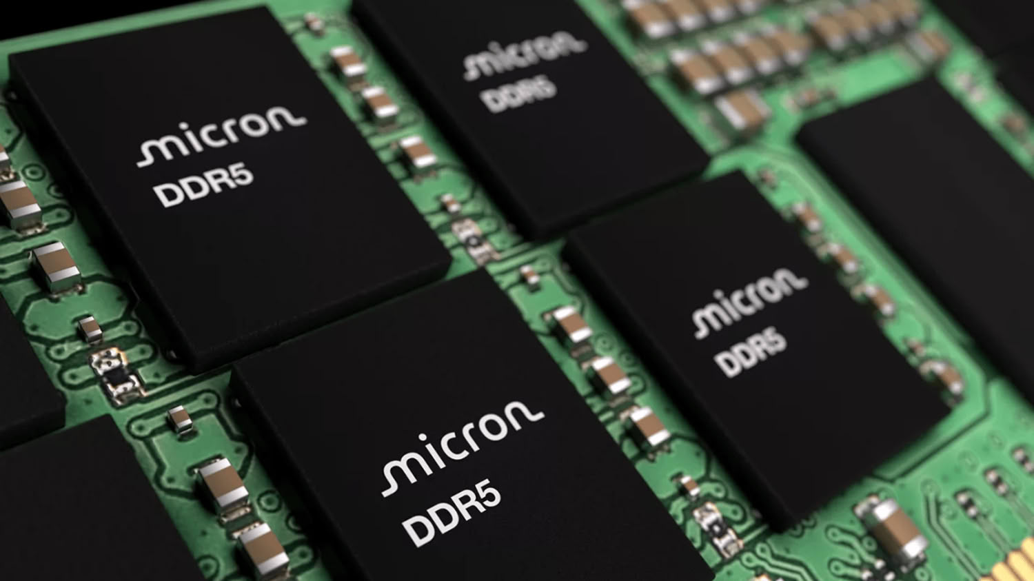
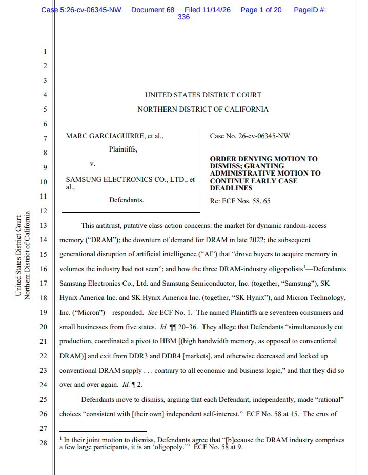
Samsung, SK hynix, and Micron Fail to Get DRAM Antitrust Suit Dismissed

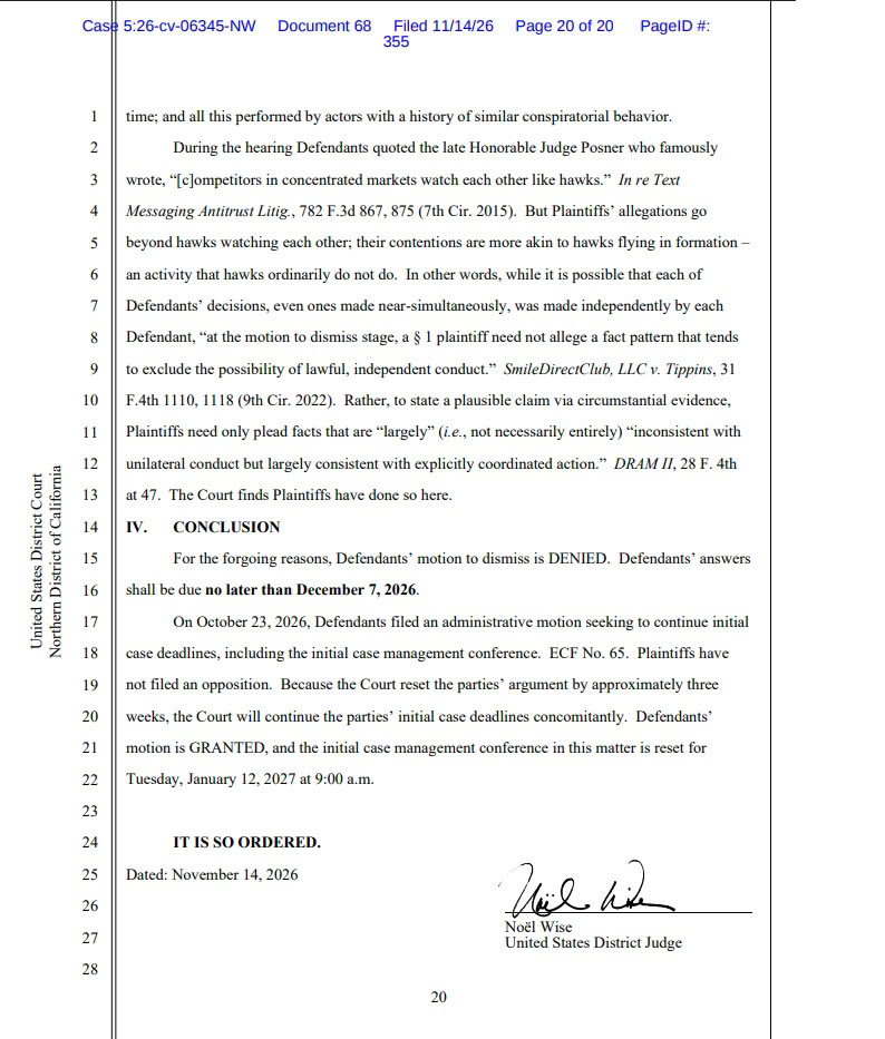
The class-action lawsuit accusing Samsung, SK hynix, and Micron of restricting DRAM supply is moving forward. On November 14, U.S. District Judge Noël Wise of the Northern District of California denied the three companies' joint motion to dismiss, finding the complaint plausibly alleges an agreement in violation of Section 1 of the Sherman Act. The suit, filed in June by 17 consumers and small businesses, claims the trio, which held over 91% of global DRAM revenue as of Q3 2025, coordinated production cuts starting in late 2022 and shifted capacity toward HBM while conventional DRAM prices rose 697% over 18 months. Of course, it's a pleading-stage ruling, and nothing has been proven yet.

The companies argued the case was a rerun of an earlier suit over 2016 to 2018 supply cuts, which the Ninth Circuit threw out in 2022. Judge Wise disagreed, pointing to newer alleged conduct like long-term HBM contracts, Samsung and SK hynix allegedly refusing long-term deals with conventional DRAM buyers, Micron shutting down Crucial, and near-identical customer vetting questions all three adopted in January 2026. She also turned the companies' own hawk comparison around, writing that the alleged conduct is more like "hawks flying in formation."

SK hynix Bets on HBM4 Demand Beyond NVIDIA With New Equipment Orders

SK hynix reportedly plans to add at least 20,000 wafers per month of HBM capacity. According to Korea's Electronic Times (ETNews), the company is in talks with equipment suppliers over a fresh round of HBM4 orders, mostly back-end tools for bonding, dicing, and inspection. Suppliers are aiming to have it all installed in the first half of 2027. The likely site is P&T6 in Cheongju, a former fab SK hynix picked for HBM in 2025. For scale, ETNews put SK hynix's total HBM capacity at around 150,000 wafers per month at the end of last year. The 20,000 figure isn't entirely new, though, since ETNews floated a similar number for P&T6 in February.

Importantly, this comes while NVIDIA is still dealing with the fallout of the Jensen Huang situation, which led to Huang resigning as CEO on November 12. Apparently, demand from AMD and Broadcom is seen as strong enough to carry HBM orders even if NVIDIA's AI business takes a hit. NVIDIA's move to lower the HBM4 speed for Vera Rubin from 11.7 Gbps to 9.6 Gbps per pin also eases the manufacturing burden for suppliers, and the report says it likely factored into the decision.

Axelera AI Unveils Titania Architecture

Axelera AI, the leading provider of purpose-built AI hardware acceleration technology, unveiled the details behind Titania, its third-generation silicon architecture in a chiplet design. Titania is highly programmable and energy efficient and will deliver high performance at interactive speeds, all within the power and cooling limits of existing data centers, rather than the 100-kilowatt-plus liquid-cooled racks that today's highest-density GPU systems require.

Performance expectations for Titania are up to 7x the throughput per watt compared to the best data center grade servers available, and up to a 20x better TCO. Each Titania-based system-in-package (SiP) will contain two Titania chiplets which are then packaged in a range of form factors, including standard PCIe cards as well as OCP-compliant UBB baseboards with eight Titania OAM modules connected in a scale-up network. In support of over $300 million in confirmed Titania commitments, these form factors will be available via OEM partners in an inference server configuration in both air- and liquid-cooled configurations.

TSMC is Reportedly Considering 3D DRAM Production

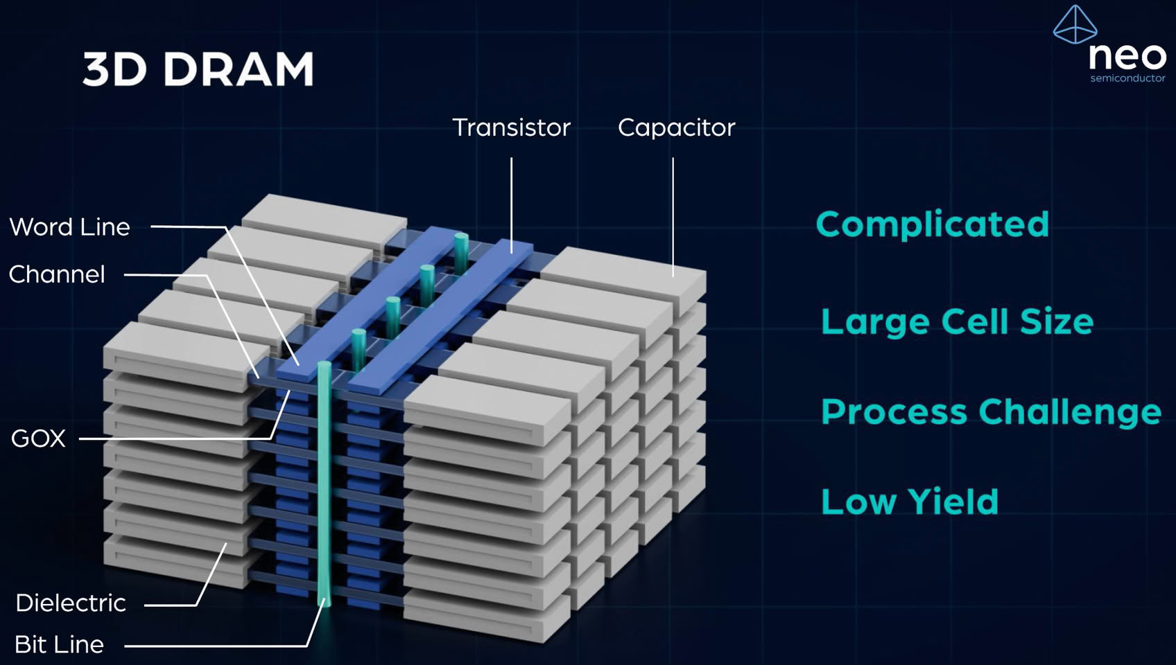
The world's largest chipmaker, TSMC, is reportedly considering entering the memory sector with the manufacturing of advanced DRAM technologies. According to a report from The Information, which cites sources close to the plans, TSMC is contemplating starting the production of 3D DRAM. As we know, there is a desperate need for more DRAM output from the three major memory makers: SK Hynix, Samsung, and Micron. New manufacturing capacity is being developed, but even when it comes online, there might still be a supply imbalance. According to The Information, TSMC is considering 3D DRAM manufacturing at the request of its largest customer, NVIDIA.

Conventional DRAM is currently produced by the big three, with plans to advance into 3D DRAM production beyond what HBM currently offers. To effectively scale memory, the 3D approach is the only way forward, as Micron recently confirmed. Micron has decided not to bring 4F² DRAM to market, even though it claims to have invented the cell design and has been researching it for around two decades, opting instead for the path to 3D DRAM. As one of the most experienced silicon manufacturers globally, TSMC is seemingly evaluating this path as well.

Samsung's 2 nm Taylor Fab 2 Reportedly Fully Booked, Mostly by AMD

Samsung has reportedly booked the entire planned output of its second fab in Taylor, Texas, and most of it is going to AMD. According to an exclusive from Korea's Maeil Business Newspaper, citing industry sources, Taylor Fab 2 will make HBM base dies for AMD and NVIDIA on a 2 nm process, with AMD's orders making up the bulk of it. Apparently, AMD's volume alone is enough to stretch the fab's capacity. Samsung declined to comment, saying it can't confirm customer-related details.

These aren't AMD's CPUs or GPUs, though. The base die is the logic chip at the bottom of an HBM stack, and Samsung plans to pair the Texas-made dies with DRAM produced in South Korea and ship them as finished HBM. Its current HBM4 and the sampled HBM4E use 4 nm base dies, so 2 nm or smaller seems aimed at later HBM generations. The deal also follows Lisa Su's visit to Samsung in October, where Samsung reportedly wanted foundry orders from AMD in return for the HBM that AMD urgently needs. A March MOU had already made Samsung the primary HBM4 supplier for the Instinct MI455X.

Qualcomm Validates HBC Silicon, Samples Appear in First Half of 2027

Qualcomm has officially validated its High Bandwidth Compute (HBC) concept, which the company showcased this summer. Instead of using traditional HBM and compute dies, Qualcomm has developed a technology that stacks multiple LPDDR layers and embeds a base die that serves as a compute engine for AI inference. In Qualcomm's San Diego lab, the first-generation HBC has achieved silicon validation with full read-write and near-memory computation capabilities. HBC utilizes LPDDR memory, stacking it across multiple layers in a 3D vertical space and interconnecting them with through-silicon vias (TSVs). This approach provides better energy efficiency than traditional HBM, which stacks regular DDR in vertical layers, as the low-power DDR (LPDDR) chips consume less power while delivering similar bandwidth and capacity.

Qualcomm has successfully stacked multiple LPDDR layers on top of each other, with the base of the HBC being a compute die that performs near-memory computation and offloads processing to near-memory dies. This technique is similar to what HBM4 memory currently does, with the base die being a logic die to better integrate compute solutions for packet tracing and data preparation for entering and exiting HBM. However, Qualcomm aims to achieve higher efficiency and more optimized data movement, with a 6x increase in bandwidth per watt compared to the current HBM specification. The goal is to have compute directly under these memory stacks so that data travels only a few microns instead of a few centimeters.

Samsung Hosts OpenAI's Sam Altman for AI Seminar, No Supply Deal Announced

Two days after arguing that the DRAM in home PCs would be put to better use in data centers, OpenAI CEO Sam Altman sat down with around 50 Samsung presidents on Saturday, October 31. The group went well past the chip business, with leaders from Samsung's finance and biotech arms joining the electronics side at the company's training center in Yongin. Samsung presented it as part of a leadership seminar series for its company-wide AI push, and the talks apparently covered where AI is headed, the markets it could open up, and how it changes the way large companies make decisions. According to Samsung, Altman told the room that adopting AI alone doesn't give anyone an edge, and that the payoff comes from using it to move faster and build better products.

Nothing came out of it in terms of a new supply contract, at least publicly, and Samsung's own write-up stuck to AI strategy. Still, it's hard to look at the visit separately from the memory shortage. Samsung signed a letter of intent with OpenAI back in October 2025 to act as a memory partner for Stargate, with OpenAI's demand projected at up to 900,000 DRAM wafers per month. Separately, on October 31, SK Group chairman Chey Tae-won also reportedly met Altman in Seoul, with SK hynix and SK Telecom executives joining, according to industry sources. Last month, AMD's Lisa Su spent hours with Samsung's chip chief chasing HBM supply, and amid all these meetings, Micron's CEO expects the memory crunch to get worse in 2027 and 2028. It seems like every major buyer is knocking on the same Korean doors.

SK hynix Expects Memory Demand to Outpace Supply Through 2030

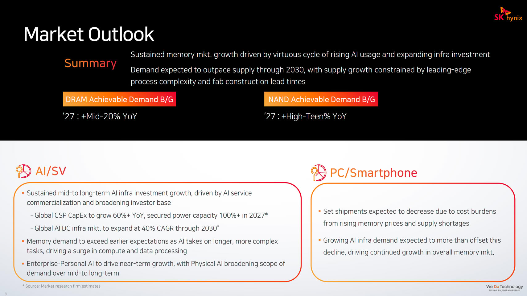
SK hynix reported its latest Q3 2026 quarterly results with a record $78.129 billion in net revenue. However, the company also shared a market outlook, highlighting its long-term supply agreements and plans for expansion with new fab capacity and facilities under construction. For the consumer market, the outlook is grim as SK hynix expects memory demand to continue outpacing supply through 2030. The main supply constraint is the complexity of leading-edge semiconductor nodes and the lengthy lead times for fab construction, which take years to translate into regular mass production volumes.

Despite sustained demand, pricing is also on an upward trajectory, with the average selling price of memory modules in Q3 increasing by over 20% compared to Q2. This is concerning, as it suggests that the prices of consumer electronics devices might jump by more than 20% once memory inventory is depleted. Although SK hynix expects a decrease in PC and smartphone shipments, this will be offset by a strong rollout of AI data centers. About 14 major customers, including most hyperscalers, have signed 5-year long-term agreements, which will account for over 50% of total capacity sold for 2027 and 2028.

NVIDIA Cuts HBM4 Speed and NVLink Bandwidth Targets for "Vera Rubin"

NVIDIA has officially implemented changes across its "Vera Rubin" product line, reducing target specifications for memory and interconnect fabric. According to the updated product specification sheet, the first change involves HBM4 memory. Previously, NVIDIA used HBM4 with a speed of 11.7 Gbps per pin, which has now been reduced to 9.6 Gbps per pin. In a "Vera Rubin" NVL72 rack-scale solution, NVIDIA now offers a total memory bandwidth of 1,400 TB/s, down from the previously advertised 1,580 TB/s. While this issue does not stem directly from NVIDIA's suppliers, it indicates that the company's implementation of memory bus width and overall electrical signaling is insufficient to support higher speeds.

However, the changes are not limited to memory. NVIDIA has also reduced the previously advertised NVLink bandwidth per GPU, decreasing it from 1.8 TB/s to 1.5 TB/s. This results in a reduction from 3.6 TB/s to 3 TB/s in bidirectional NVLink GPU bandwidth. The underlying issue is related to signal integrity, as NVIDIA reportedly lowered the NVLink Nyquist frequency target from 56 GHz to 47 GHz. Lowering the Nyquist frequency reduces the electrical demands on the SerDes, cables, and materials, which can improve manufacturing yields and overall feasibility, even though it requires accepting a small reduction in peak interconnect bandwidth. Thus, NVIDIA chose to sacrifice some bandwidth to enhance system stability. Below is the new system specification in light mode, and old system specification in dark mode.

Dell CEO Says the Memory Shortage Will Get Worse in 2027

Michael Dell doesn't think the memory shortage is anywhere near over. Speaking with The Wall Street Journal, Dell's chairman and CEO said things will get worse next year, as the AI data center buildout keeps soaking up DRAM and HBM supply. According to him, the bottleneck for Dell isn't demand, since the company is sitting on roughly $95 billion worth of AI server orders it hasn't delivered yet, the largest backlog in its history. Memory is what's holding those shipments back, as AI accelerators need plenty of HBM, while the servers around them still rely on conventional DRAM.

Relief also looks quite far away. New memory fabs take around four years to build, so Dell apparently doesn't expect meaningful new supply until 2029 or 2030. That aligns with Micron's CEO, who recently said supply will be much tighter in 2027 and 2028 than it is this year. Interestingly, SK hynix's CEO said something similar, expecting the memory shortage to last through 2030. Dell is reportedly coping by buying DRAM only when final assembly is close and by locking in long-term supply agreements, though there's no word on how much of that applies to its consumer products.

Samsung Taps TSMC for NVHBM Base Die Production

Samsung is reportedly collaborating with the world's largest chip maker, TSMC, to secure a base die supply for NVIDIA's newly announced NVHBM memory standard. NVHBM integrates the controller into the 3D HBM stack, significantly enhancing performance and efficiency. Compared to standard HBM4E, NVIDIA claims up to 30% more memory bandwidth, 15% lower HBM power consumption, and up to 25% more usable compute die area on the processing unit. In simple terms, NVHBM builds on the standard HBM architecture with base die customization, but there are a few strict requirements that must be fulfilled before mass production.

Interestingly, one of the requirements is that NVIDIA's base die in the NVHBM must be manufactured on TSMC's 3 nm node. Even though Samsung has its own 3 nm production lines, NVIDIA's IP is optimized for TSMC's nodes. This forces Samsung to collaborate with TSMC and become a customer, despite having its own production capabilities. However, this arrangement is only for the base die, which integrates directly next to the compute tiles. For memory, Samsung will continue using its sixth-generation 10 nm processes, which are typical for HBM manufacturing. This means that only part of the production will be handled by TSMC.

AMD CEO Visits Samsung for HBM, Samsung Wants Foundry Orders in Return

AMD CEO Dr. Lisa Su reportedly visited Samsung on October 7th and spent about three hours with Samsung chip chief Jun Young-hyun in Seoul on Wednesday, and a Korean media report suggests the two sides want different things from each other. As relayed by @jukan05 on X, Samsung apparently wants AMD to place orders with Samsung Foundry in return for HBM and other memory, which AMD urgently needs. A senior semiconductor industry official quoted in the report said "AMD sees entrusting its foundry work to Samsung Electronics as too risky," and added that this gap is what brought about the talks. Neither company has confirmed any of it, so it is best treated as an industry report for now.

Su's public comments were far more diplomatic. Speaking to Reuters and other reporters in Seoul ahead of the meeting, she said AMD continues to explore opportunities with Samsung in both memory and foundry. Asked directly whether AMD would build chips at Samsung, she stopped short of confirming any plans. She was more direct about memory, urging suppliers to "build faster, as fast as possible" and noting that AMD is working with customers to trim their memory footprint.

Samsung HBM4E Passes Testing for NVIDIA's "Rubin Ultra" GPU

Samsung's upcoming HBM4E memory has reportedly passed testing for NVIDIA's next-generation "Rubin Ultra" AI GPU accelerator family. This is great news for the company, as its previous HBM3E didn't meet NVIDIA's requirements, leading NVIDIA to choose Samsung for GDDR7 only, instead of HBM3E. The new HBM generation brings significant advancements, and Samsung is one of the leading manufacturers with designs currently running at 14 Gbps per pin and 2,048 pins per HBM4E stack. Samsung can achieve a maximum bandwidth of 3.6 TB/s, and at 16 Gbps, this maximum memory bandwidth will increase to 4 TB/s for a single HBM4E stack.

With about a dozen memory stacks per AI accelerator or GPU, the total memory bandwidth will be remarkable. The company is currently offering this memory in a 12-layer (or 12-high) configuration with a memory density of 48 GB per stack. However, customer requirements will also include 8-layer 32 GB and 16-layer 64 GB stacks in the future.

SK hynix Reportedly Faces Difficulties in HBM Hybrid Bonding, Trailing Samsung

According to a process development engineer at SK hynix's future technology research institute, who spoke with Damnang, SK hynix is reportedly facing challenges in developing hybrid bonding technology for its HBM memory. These issues are significant enough that SK hynix has not yet begun production of samples, while Samsung has reportedly already sent out samples of HBM manufactured using hybrid bonding to customers. If true, this represents a major setback for SK hynix, whose HBM has held the top spot in global market share by revenue. This could potentially lead to a loss of market share among customers who require higher capacities, better performance, and more advanced technology from their HBM suppliers.

For those unfamiliar, hybrid bonding creates a permanent bond between two silicon chips using embedded metal bumps that are fused together to form a single chip. Multiple dies or entire silicon wafers can be connected by stacking the back ends of two chips together. This technology eliminates traditional chip bumps and directly bonds copper interconnections between the two chips. Essentially, hybrid bonding can create shorter distances, reducing latency and improving performance, lowering signal distortion, and offering many other benefits.

Samsung Foundry to Manufacture Anthropic AI ASIC on 2 nm Node

Samsung Foundry may be on the verge of securing a significant deal with AI lab Anthropic to manufacture AI accelerators. According to the latest report, Anthropic is developing its custom AI accelerator on Samsung's SF2 2 nm node, which will initially be produced in a lower volume of around 200,000 chips. The design and implementation of this ASIC are being handled by Broadcom, targeting around 4,000 TOPS of INT8 compute, with a TDP of 1,300 W per chip. This will be supported by either 192 GB of HBM3E or even 288 GB of HBM3E, if the design allows. The current production volume is low, as ASIC projects are typically counted in millions of chips. However, Anthropic is likely evaluating the project's viability, which requires a complete custom infrastructure with networking, rack design, power supply, cooling, and many other factors.

The current Samsung SF2 node is built using Low-NA EUV lithography and is manufactured in South Korea, with a new facility soon to be established in Taylor, Texas. For packaging these chips and integrating them with HBM, Samsung is likely to employ its I-Cube technology, which rivals TSMC's CoWoS and allows for 2.5D packaging. Combined with the 2 nm dies, Samsung can position itself as a serious manufacturing plant for external customers and slightly close the gap with TSMC and its contract manufacturing business.

NVIDIA Could Account for 37% of 2027 HBM Capacity, Worth $279 Billion

NVIDIA's supply commitments climbed to $279 billion in the quarter ended July 26, up from $119 billion the quarter before. The company says the increase is primarily related to memory procurement. Morgan Stanley estimates that NVIDIA has claimed about 37.3% of global high-bandwidth memory (HBM) supply for 2027, with Alphabet at 36% and AMD at 12.1%. That adds up to roughly 85%, leaving everyone else to split the rest. These are Morgan Stanley's estimates, as reported by The Inference.

About $267 billion of the commitments come due by the end of fiscal 2029, according to the filing. NVIDIA reported record revenue of $96.2 billion for the quarter, but memory costs are weighing on margins. Gross margin was 75% and is guided to 74% this quarter, with a trough of 71% to 72% expected in the January quarter. CFO Colette Kress tied that pressure to memory pricing. Operating cash flow also fell to $24.1 billion from $50.3 billion the quarter before. Jensen Huang said on September 17 that he expects NVIDIA to sell twice as many chips next year, and the company's formal guidance is about 70% revenue growth.

Samsung to Double HBM4 and HBM4E Capacity in 2027 Amid Strong Demand

Samsung is reportedly increasing its orders for materials to boost high-bandwidth memory (HBM) production, with plans to double the production capacity of its current HBM4 and HBM4E manufacturing by 2027. According to SE Daily, the manufacturing capacity for HBM4 and HBM4E is expected to grow from around 20,000 wafers per month in 2026 to 50,000 wafers per month in 2027. This data is derived from the use of glass carriers, which are temporary glass panels placed over thin DRAM wafers to prevent warping or breaking as they are prepared for packaging. Since HBM involves stacking many thin DRAM modules, glass carriers stabilize these wafers until the packaging process begins and the glass is removed. As the unit is one glass carrier per wafer, this provides an estimate of how many HBM4 and HBM4E wafers are produced each month.

Additionally, Samsung's overall HBM production, which includes older generations like HBM3 and HBM3E, currently averages around 180,000 wafers this year and is expected to grow to about 250,000 HBM wafers next year, with 80% dedicated to HBM4 and HBM4E. Samsung began mass production of HBM4 on its sixth-generation 10 nm-class 1c node in February, with HBM4E customer samples available by mid-2026. Future production increases will focus on HBM4 and HBM4E, as customers seek higher densities and bandwidth for their AI accelerators.

AI Chip Packaging Pushes Beyond Reticle Limits, with CoWoS-L Set to Remain the Mainstream Advanced Packaging Solution Through 2028

TrendForce's latest research into advanced semiconductor packaging reveals that GPU suppliers and hyperscale CSPs are continuing to develop increasingly powerful and versatile AI chips, making larger package sizes a key development priority for 2.5D packaging. Although TSMC's CoWoS-L faces competition from Intel's EMIB-T, its advantages in technology maturity and yield are expected to keep it the mainstream packaging solution for AI chips through 2028.

TrendForce notes that strong AI demand continues to support NVIDIA's push toward integrated GB/VR rack-scale solutions, which incorporate large numbers of chips. NVIDIA's high-end GPU shipments are expected to grow approximately 30% YoY in 2026. AMD, meanwhile, is aggressively promoting its MI400/MI450 series beginning in the second half of 2026, providing further momentum to overall shipments.

Intel and SK hynix Could Start DRAM Production in United States

According to anonymous sources close to Reuters, Intel and SK hynix are in talks to start DRAM production lines in the United States for the first time. This means that Intel might either collaborate with SK hynix to acquire memory IP technology in a joint venture or SK hynix could lease part of Intel's facility in Ohio. In the first scenario, a joint venture between Intel and SK hynix would significantly alleviate supply chain pressures, as hyperscalers, fabless chip designers, and others are in urgent need of more DRAM. Since these firms would likely consume all the DRAM produced in the coming years, both Intel and SK hynix would have a substantial financial interest in the joint venture.

On the other hand, if SK hynix decides to lease Intel's facilities in Ohio, the South Korean memory giant would pay premiums for leasing the facility while retaining all production for itself. Reuters couldn't determine which specific technology would be the focus of the facility, but the primary goal is to produce regular planar DRAM, HBM, and some storage solutions with NAND Flash. Intel declined to comment on the rumor but noted that the Ohio investments are continuing regardless. SK hynix stated that the company has not finalized its decision or any cooperation but did not explicitly rule out the possibility of future collaboration. Therefore, an official decision should be announced soon.

Kepler Computing Emerges to Build HBM Alternative Using FeRAM

After seven years of operating in stealth mode, a new startup called Kepler Computing has emerged to address the memory crisis using a custom memory technology. The startup claims to have developed an alternative to HBM using a new 3D stacking technique and novel materials, all without relying on cutting-edge semiconductor nodes. Kepler reportedly plans to use ferroelectric RAM (FeRAM). This use of FeRAM is said to allow Kepler to maintain the standard HBM capacity while significantly reducing manufacturing costs. The company has reportedly overcome many challenges in scaling production and has undergone 35 iterations of composites before settling on a single scalable design.

While modern memory production typically requires EUV lithography, Kepler intends to use existing mature nodes to manufacture HBM and SRAM using FeRAM. In early collaborations with GlobalFoundries, Kepler managed to convert a standard 28 nm manufacturing facility into a memory fab in just eight months, which is significantly faster than the typical 24-month lead time for traditional DRAM. Currently, the company has processed about 2,000 wafers of the new DRAM technology, with the first HBM samples expected to arrive later this year. For full-scale volume manufacturing, the company aims to begin production runs at GlobalFoundries' Singapore facility next year, with manufacturing in the United States slated to start in 2028.

CXMT Reportedly Struggles With HBM3E, Yields Are Only 25%

Chinese memory giant CXMT is reportedly facing difficulties with HBM3 production, according to South Korean media. Late last month, it was revealed that CXMT had begun risk production of HBM3E memory, lagging two generations behind Samsung, SK hynix, and Micron, who are already progressing with HBM4E sampling. At that time, it was known that the company was conducting HBM3E risk production in limited runs, but details were scarce. However, today we learn that three out of four HBM3E stacks are defective, indicating that CXMT currently operates at a 25% yield. Stacking DRAM is a complex task, as the technology required is much more intricate than planar DRAM manufacturing, an area where CXMT reportedly excels.

The low yields are reportedly due to the immaturity of the through-silicon via (TSV) technology that CXMT employs. In front-end manufacturing, CXMT achieves around 30% yields, while back-end processing yields about 70% on top of the original 30%. For instance, Samsung uses about 5,000 TSVs per layer on HBM2, and SK hynix uses more than 8,000 TSVs per layer on its HBM3. However, data suggests that CXMT is attempting to achieve HBM3E with only 3,000 TSVs per layer and is trying to pack 8 layers in the regular 8-Hi HBM3E configuration. Given these challenges, the company is unlikely to transition to a higher-capacity 12-Hi HBM in the near term as it addresses engineering challenges.

SK hynix Boosts Leading-Edge 1c DRAM Production to a Dominant Position

SK hynix is shifting much of its capacity to the latest 1c DRAM node, according to recent reports. The South Korean giant is transitioning the bulk of its memory production between nodes, and as DRAM technology advances, the company is moving its production to more advanced 10 nm-class nodes. For SK hynix, the sixth-generation 10 nm class 1c DRAM node accounted for 10% of production in Q1 2026, with an increase to about 13% in Q2. In the current third quarter, the company is expected to manufacture 24% of its DRAM on 1c, while Q4 will see more than a third (34%) produced on that node. By Q1 2027, the 1c node will account for around 35%, making the fifth-generation 10 nm-class 1b node at 33%, officially SK hynix's most dominant node.

As a reminder, DRAM nodes are not the same as conventional logic nodes. DRAM manufacturers use variations of 10 nm and scale them with more EUV layers or advanced features. For SK hynix, the currently dominant 1b node is around 12-13 nm in actual design and involves about 4 layers of EUV patterning, while the most advanced 1c node shrinks to 11-12 nm with 5-6 layers of EUV. SK hynix will use the 1c node to manufacture HBM4E, LPDDR6, and DDR5 memory. For the older 1b node, SK hynix produces DDR5, LPDDR5X, HBM3E, and HBM4.

DRAM Industry Revenue Rises 59.5% QoQ in 2Q26 as Supply Expansion Continues to Lag Demand Growth

TrendForce's latest findings on the memory industry reveal that sharp rises in traditional DRAM contract prices have led to a 59.5% QoQ increase in total DRAM industry revenue, reaching nearly US$154.73 billion in 2Q26.

Growing demand for AI servers, fueled by expanding LLM training and AI inference, has driven higher shipments of HBM3e, LPDDR5X, and high-capacity RDIMMS. The surge in agentic AI applications is further boosting RDIMM demand across various capacities.

Samsung Foundry Allocates Half of 4 nm Capacity for HBM4 Base Dies

According to Korean media, Samsung Foundry, a division that operates silicon manufacturing as a subsidiary of Samsung Electronics, is reportedly allocating significant capacity for HBM4 base die manufacturing. For HBM4, Samsung is producing the base die on a 4 nm node, which reportedly receives half of the entire manufacturing capacity of the 4 nm node, internally referred to as SF4. Customers of HBM4 and the upcoming HBM4E memory standards are now requesting base dies to be filled with custom logic. For instance, customers could implement custom logic like memory controllers and PHYs directly on the HBM base die, significantly reducing the area occupied by these components on the main compute chiplet.

Samsung operates its SF4 manufacturing at Pyeongtaek Campus 2 (P2) and Campus 3 (P3) on lines S5 and S6. An increase in manufacturing is not only coming for ASIC designs by external customers but also for HBM4 base die manufacturing, which is becoming especially important for ASIC customers aiming to maximize the performance of their designs.
Return to Keyword Browsing
Nov 17th, 2026 13:53 CST change timezone

New Forum Posts

Popular Reviews

TPU on YouTube

Controversial News Posts