News Posts matching #SoC

Return to Keyword Browsing

Xilinx Collaborates with Fujitsu to Support 5G Deployments in the US

Xilinx, Inc.,, the leader in adaptive computing, today announced that the company is supplying its leading UltraScale+ technology to Fujitsu Limited for its O-RAN 5G radio units (O-RUs). Fujitsu O-RUs using Xilinx technology will be deployed in the first O-RAN-compliant 5G greenfield networks in the U.S. Fujitsu is also evaluating Xilinx RFSoC technology to further reduce cost and power consumption for additional future site deployments.

Fujitsu O-RUs are ideal for a broad-range of spectrum and multi-band applications for 5G O-RAN networks. The Xilinx UltraScale+ devices used within Fujitsu O-RUs deliver the best balance of cost economies as well as the adaptability and scalability required for the evolving needs of 5G O-RAN network requirements. Additionally, Xilinx will continue to work with other O-RAN ecosystem partners to ensure continued validation of the hardware and software necessary for world-class 5G networks.
Samsung Exynos SoC with AMD RDNA GPU Destroys Competition, Apple 14 Bionic SoC Kneels

Some time ago, Samsung and AMD announced that they will be building a mobile processor that utilizes AMD RDNA architecture for graphics processing. Samsung is readying its Exynos 2100 SoC and today we get to see its performance results in the first leaked benchmark. The new SoC design has been put through a series of GPU-only benchmarks that stress just the AMD RDNA GPU. Firstly there is Manhattan 3 benchmark where the Exynos SoC scored 181.8 FPS. Secondly, the GPU has scored 138.25 FPS in Aztek Normal and 58 FPS in Aztek High. If we compare those results to the Apple A14 Bionic chip, which scored 146.4 FPS in Manhattan 3, 79.8 FPS in Aztek Normal, and 30.5 FPS in Aztek High, the Exynos design is faster anywhere from 25% to 100%. Of course, given that this is only a leak, all information should be taken with a grain of salt.

Apple Patents Multi-Level Hybrid Memory Subsystem

Apple has today patented a new approach to how it uses memory in the System-on-Chip (SoC) subsystem. With the announcement of the M1 processor, Apple has switched away from the traditional Intel-supplied chips and transitioned into a fully custom SoC design called Apple Silicon. The new designs have to integrate every component like the Arm CPU and a custom GPU. Both of these processors need good memory access, and Apple has figured out a solution to the problem of having both the CPU and the GPU accessing the same pool of memory. The so-called UMA (unified memory access) represents a bottleneck because both processors share the bandwidth and the total memory capacity, which would leave one processor starving in some scenarios.

Apple has patented a design that aims to solve this problem by combining high-bandwidth cache DRAM as well as high-capacity main DRAM. "With two types of DRAM forming the memory system, one of which may be optimized for bandwidth and the other of which may be optimized for capacity, the goals of bandwidth increase and capacity increase may both be realized, in some embodiments," says the patent, " to implement energy efficiency improvements, which may provide a highly energy-efficient memory solution that is also high performance and high bandwidth." The patent got filed way back in 2016 and it means that we could start seeing this technology in the future Apple Silicon designs, following the M1 chip.

Update 21:14 UTC: We have been reached out by Mr. Kerry Creeron, an attorney with the firm of Banner & Witcoff, who provided us with additional insights about the patent. Mr. Creeron has provided us with his personal commentary about it, and you can find Mr. Creeron's quote below.

MediaTek Launches 6nm Dimensity 1200 Premium 5G SoC

MediaTek today unveiled its new Dimensity 1200 and Dimensity 1100 5G smartphone chipsets with unrivaled AI, camera and multimedia features for powerful 5G experiences. The addition of the 6 nm Dimensity 1200 and 1100 chipsets to MediaTek's 5G portfolio gives device makers a growing suite of options to design highly capable 5G smartphones with top of the line camera features, graphics, connectivity enhancements and more.

"MediaTek continues to expand its 5G portfolio with highly integrated solutions for a range of devices from the high-end to the mid-tier," said JC Hsu, Corporate Vice President and General Manager of MediaTek's Wireless Communications Business Unit. "Our new Dimensity 1200 stands out with its impressive 200MP camera support and advanced AI capabilities, in addition to its innovative connectivity, display, audio and gaming enhancements."

Apple M1 & A14 Die Shot Comparison Shows Differences in SoC Design

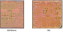
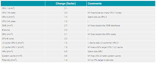
When Apple first announced the M1, questions arose about the differences between it and the A14 chip which both share many architectural features and are both manufactured on TSMC's 5 nm process. Semiconductor analysis firm TechInsights has recently published die photos of the two processors and a summary of the changes.

The M1 features four high-performance Firestorm cores and four energy-efficient IceStorm cores for a total of eight CPU cores. The A14 only features six CPU cores with two high-performance Firestorm cores and four energy-efficient IceStorm cores. The M1 includes doubles the amount of GPU cores and DDR interfaces then found on the A14. The M1 also incorporates silicon not found on the A14 including the Apple T2 security processor and other controllers. These additions result in a die size 37% larger than the A14.

Akasa Rolls Out Turing A50 Case for ASUS PN50 Ryzen 4000-powered Mini PC

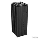
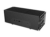
Akasa ended the year with the release of the Turing A50, a fanless all-aluminium case with which you can replace the case that comes with the ASUS PN50 mini-PC. The ASUS PN50, if you recall, is a NUC-sized mini-PC that uses 15-Watt AMD Ryzen 4000-series "Renoir" mobile processors. The Akasa Turing A50 is a variation of the original Turing NUC case the company released back in February 2019, but with its innards re-designed for the ASUS PN50 mainboard. On the front side, you get mounts for the board's headset jack, two USB 3.2 ports (from which one is type-C and has DisplayPort passthrough), and the IR receiver. The rear has mounts for the three other display outputs, and a couple more USB ports, and the DC power input. Internally, the case features an SoC cooler base designed to mount onto the "Renoir" SoC, from which a few copper heat-pipes convey heat to the case's aluminium body, which doubles up as a heatsink. Fanless Tech reports that the case should be available from February 2021.

Intel Debuts 2nd-Gen Horse Ridge Cryogenic Quantum Control Chip

At an Intel Labs virtual event today, Intel unveiled Horse Ridge II, its second-generation cryogenic control chip, marking another milestone in the company's progress toward overcoming scalability, one of quantum computing's biggest hurdles. Building on innovations in the first-generation Horse Ridge controller introduced in 2019, Horse Ridge II supports enhanced capabilities and higher levels of integration for elegant control of the quantum system. New features include the ability to manipulate and read qubit states and control the potential of several gates required to entangle multiple qubits.

"With Horse Ridge II, Intel continues to lead innovation in the field of quantum cryogenic controls, drawing from our deep interdisciplinary expertise bench across the Integrated Circuit design, Labs and Technology Development teams. We believe that increasing the number of qubits without addressing the resulting wiring complexities is akin to owning a sports car, but constantly being stuck in traffic. Horse Ridge II further streamlines quantum circuit controls, and we expect this progress to deliver increased fidelity and decreased power output, bringing us one step closer toward the development of a 'traffic-free' integrated quantum circuit."-Jim Clarke, Intel director of Quantum Hardware, Components Research Group, Intel.

Intel Sells Its Power Management Chip Business, Enpirion, to Mediatek for $85 Million

Intel continues to "shed fat" on its business portfolio. After last year's sale of its smartphone modem chip business to Apple, the company is now parting ways with its power management circuitry division - Enpirion - and offloading it to Richtek, a division of Taiwanese MediaTek. The sale price of $85 million is a drop in the bucket for Intel's overall bottom line, so it's not a way for the company to cash in some desperately needed money - all accounts of Intel's troubles in the wake of its semiconductor manufacturing issues and AMD's market resurgence pale in comparison to Intel's revenues.

This actually looks like a company that's actually streamlining its R&D expenditures and focusing on execution for the markets Intel sees as most important for today and for tomorrow. Intel's Enpirion focuses on building power management chips for FPGA circuits, SoCs, CPUs, and ASICs, and will now serve to bolster MediaTek's SoC business while allowing the Taiwanese company to expand and diversify its business portfolio, even as Intel focuses on their core competencies.

Samsung Could Become Apple's Newest Chip Supplier

Apple has recently announced its transition to Apple Silicon, meaning that every processor inside its products will be custom designed by the company. However, that seems to be becoming a bit of a problem. The sole supplier of chips for Apple has been Taiwan Semiconductor Manufacturing Company (TSMC), which Apple collaborated with for the past few years. The sheer capacity of TSMC is enough to satisfy the demand from several companies and thus it allows some of them to book its capacity. With Apple demanding more and more capacity than ever before, it is becoming quite hard to keep up with it. That is why Apple is, according to some analysts for Business Korea, looking for a foundry beyond TSMC's to manufacture its chips.

According to the source, Apple is looking at the direction of Samsung Electronics and its silicon manufacturing facilities. Samsung has recently started the production of its 5 nm silicon manufacturing node. We have reported that the first SoCs are set to arrive soon. However, it may be possible that Apple's M1 lineup of SoCs will be a part of that first wave. Apple is reportedly going to tap both TSMC and Samsung to qualify enough supply for the huge demand of the products based on the latest 5 nm technology.

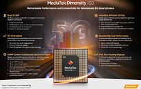
MediaTek Announces Dimensity 700 SoC For Mass Market 5G Smartphones

MediaTek today unveiled its new Dimensity 700 5G smartphone chipset, a 7 nm SoC designed to bring advanced 5G capabilities and experiences to the mass market. The addition of the Dimensity 700 to MediaTek's Dimensity family of 5G chips gives device makers a full suite of options for 5G smartphone models - from flagship and premium to mid-range and mass market devices - making 5G more accessible for consumers everywhere.

"With our expanded Dimensity portfolio we're bringing the latest 5G capabilities to every smartphone tier so more people can enjoy 5G experiences," said Dr. JC Hsu, Corporate VP and GM of MediaTek's Wireless Communications Business Unit. "The Dimensity 700 has an impressive mix of 5G connectivity features, advanced camera capabilities like night shot enhancements and multiple voice assistant support, all in a super power-efficient design."

Apple Could Unveil Arm-powered MacBooks on November 10

Apple late Monday sent out a public invite to an online launch event dated November 10, without revealing what it is. With new generation iPhones and Watches and iPads already announced it's likely that the November 10 event could deal with Macs, specifically, the company's very first MacBooks powered by a non-Intel processor since the company embraced x86 some decade-and-a-half ago.

Apple, having gained in-house expertise in designing powerful Arm-based SoCs, is likely to debut a new Arm-based processor with sufficient muscle to drive MacBooks, in what will be a "client-first" strategy of replacing x86 with Arm for Apple. This will likely see the most client-segment products, such as MacBooks and Mac Mini, get the processor, followed by MacBook Pros, iMacs, and lastly workstation-segment products such as the Mac Pro and iMac Pro. The November 10 event will likely only cover the very first Arm-powered MacBooks. Apple has been selling Arm-powered Mac Minis to ISVs along with a special version of macOS "Big Sur," so they could port their Mac software to the new platform. Arm-powered Macs could also see some form of unification between the iOS and macOS software ecosystems.

Samsung's 5 nm Node in Production, First SoCs to Arrive Soon

During its Q3 earnings call, Samsung Electronics has provided everyone with an update on its foundry and node production development. In the past year or so, Samsung's foundry has been a producer of a 7 nm LPP (Low Power Performance) node as its smallest node. That is now changed as Samsung has started the production of the 5 nm LPE (Low Power Early) semiconductor manufacturing node. In the past, we have reported that the company struggled with yields of its 5 nm process, however, that seems to be ironed out and now the node is in full production. To contribute to the statement that the new node is doing well, we also recently reported that Samsung will be the sole manufacturer of Qualcomm Snapdragon 875 5G SoC.

The new 5 nm semiconductor node is a marginal improvement over the past 7 nm node. It features a 10% performance improvement that is taking the same power and chip complexity or a 20% power reduction of the same processor clocks and design. When it comes to density, the company advertises the node with x1.33 times increase in transistor density compared to the previous node. The 5LPE node is manufactured using the Extreme Ultra-Violet (EUV) methodology and its FinFET transistors feature new characteristics like Smart Difusion Break isolation, flexible contact placement, and single-fin devices for low power applications. The node is design-rule compatible with the previous 7 nm LPP node, so the existing IP can be used and manufactured on this new process. That means that this is not a brand new process but rather an enhancement. First products are set to arrive with the next generation of smartphone SoCs, like the aforementioned Qualcomm Snapdragon 875.

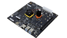
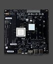
RISC-V Comes to PC: SiFive Introduces HiFive Unmatched Development Board

RISC-V architecture is a relatively new Instruction Set Architecture (ISA) developed at the University of California Berkeley. Starting as a "short, three-month project" the RISC-V ISA is a fifth generation of the Reduced Instruction Set Computing (RISC) ideology. A company working on this technology and helping to grow the ecosystem is SiFive. Today, they announced a big step forward for the ecosystem that will enable developers to make and optimize even more software for this architecture and platform. Called the HiFive Unmatched, the development board represents the first entry of RISC-V ISA to the world of personal computing, with its Mini-ITX form factor and PC-like connectors of power supply and I/O.

The board is home to SiFive's FU740 SoC, a five-core heterogeneous, coherent processor with four SiFive U74 cores, and one SiFive S7 core. This SoC is capable of smooth Linux OS operation, giving the developers a good platform to do their optimizations for. There is 8 GB of onboard DDR4 RAM (unknown frequencies and timing), a MicroSD card slot, and one PCIe 3.0 x4 M.2 slot for system storage. To connect the board to the outside world, you get one Gigabit Ethernet port. For user I/O there are four USB 3.2 Gen 1 Type-A ports (1 Charging port) and one MicroUSB Console port. To power the board, you need a proper power supply with a 24-pin power connector. If you plan to build a PC based on the Unmatched board, you would need a standard ITX case, as it comes in the standard Mini-ITX (170x170 mm) form factor. For more information, please check out SiFive's website.

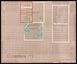
Apple A14 SoC Put Under the Microscope; Die Size, and Transistor Density Calculated

Apple has established itself as a master of silicon integrated circuit design and has proven over the years that its processors deliver the best results, generation after generation. If we take a look at the performance numbers of the latest A14 Bionic, you can conclude that its performance is now rivaling some of the x86_64 chips. So you would wonder, what is inside this SoC that makes it so fast? That is exactly what ICmasters, a semiconductor reverse engineering and IP services company, has questioned and decided to find out. For starters, we know that Apple manufactures the new SoCs on TSMC's N5 5 nm node. The Taiwanese company promises to pack 171.3 million transistors per square millimeter, so how does it compare to an actual product?

ICmasters have used electron microscopy to see what the chip is made out of and to measure the transistor density. According to this source, Apple has a chip with a die size of 88 mm², which packs 11.8 billion N5 transistors. The density metric, however, doesn't correspond to that of TSMC. Instead of 171.3 million transistors per mm², the ICmasters measured 134.09 million transistors per mm². This is quite a difference, however, it is worth noting that each design will have it different due to different logic and cache layout.
Apple A14 SoC Die Apple A14 SoC

Microsoft: Only Consoles Supporting Full RDNA 2 Capabilities Are Xbox Series X and Series S, Excludes PlayStation 5

Microsoft has today published another article on its Xbox Wire blog, dedicated to all the news regarding the Xbox consoles and its ecosystem. In the light of yesterday's launch of AMD Radeon RDNA 2 graphics cards, Microsoft has congratulated its partner and provider of processors SoCs for their next-generation consoles. Besides the celebrations and congratulations, Microsoft has proceeded to show off what the Xbox Series X and Series S consoles are capable of, and how they integrate the RDNA 2 architecture. The company notes that there are hardware accelerated DirectX Raytracing, Mesh Shaders, Sampler Feedback, and Variable Rate Shading units built-in, so game developers can take advantage of it.

Another interesting point Microsoft made was that "Xbox Series X|S are the only next-generation consoles with full hardware support for all the RDNA 2 capabilities AMD showcased today." What this translates into is that Microsoft is the only console maker that uses the full RDNA 2 potential. This could leave Sony out in the dark with its PlayStation 5 console, meaning that it does not support all the features of AMD's new GPU architecture. There are not any specific points, however, we have to wait and see what Sony has left out, if anything.

Dialog Semiconductor Licenses its Non-Volatile ReRAM Technology to GLOBALFOUNDRIES for 22FDX Platform

DIALOG SEMICONDUCTOR, a leading provider of battery and power management, Wi-Fi and Bluetooth low energy (BLE) and Industrial edge computing solutions and GLOBALFOUNDRIES (GF ), the world's leading specialty foundry, today announced that they have entered into an agreement in which Dialog licenses its Conductive Bridging RAM (CBRAM) technology to GLOBALFOUNDRIES. The resistive ram (ReRAM)-based technology was pioneered by Adesto Technologies which was recently acquired by Dialog Semiconductor in 2020. GLOBALFOUNDRIES will first offer Dialog's CBRAM as an embedded, non-volatile memory (NVM) option on its 22FDX platform, with the plan to extend to other platforms.

Dialog's proprietary and production proven CBRAM technology is a low power NVM solution designed to enable a range of applications from IoT and 5G connectivity to artificial intelligence (AI). Low power consumption, high read/write speeds, reduced manufacturing costs and tolerance for harsh environments make CBRAM particularly suitable for consumer, medical, and select industrial and automotive applications. Furthermore, CBRAM technology enables cost-effective embedded NVM for advanced technology nodes required for products in these markets.

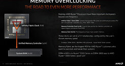
AMD Ryzen 5000 Series Features Three Synchronized Memory Clock Domains

A leaked presentation slide by AMD for its Ryzen 5000 series "Zen 3" processors reveals details of the processor's memory interface. Much like the Ryzen 3000 series "Matisse," the Ryzen 5000 series "Vermeer" is a multi-chip module of up to 16 CPU cores spread across two 8-core CPU dies, and a unified I/O die that handles the processor's memory-, PCIe, and SoC interfaces. There are three configurable clock domains that ensure the CPU cores are fed with data at the right speed, and to ensure that the MCM design doesn't pose bottlenecks to the memory performance.

The first domain is fclk or Infinity Fabric clock. Each of the two CCDs (8-core CPU dies) has just one CCX (CPU core complex) with 8 cores, and hence the CCD's internal Infinity Fabric cedes relevance to the IFOP (Infinity Fabric over Package) interconnect that binds the two CCDs and the cIOD (client I/O controller die) together. The next frequency is uclk, or the internal frequency of the dual-channel DDR4 memory controller contained in the cIOD. And lastly, the mclk, or memory clock is the industry-standard DRAM frequency.

Arm Highlights its Next Two Generations of CPUs, codenamed Matterhorn and Makalu, with up to a 30% Performance Uplift

Editor's Note: This is written by Arm vice president and general manager Paul Williamson.

Over the last year, I have been inspired by the innovators who are dreaming up solutions to improve and enrich our daily lives. Tomorrow's mobile applications will be even more imaginative, immersive, and intelligent. To that point, the industry has come such a long way in making this happen. Take app stores for instance - we had the choice of roughly 500 apps when smartphones first began shipping in volume in 2007 and today there are 8.9 million apps available to choose from.

Mobile has transformed from a simple utility to the most powerful, pervasive device we engage with daily, much like Arm-based chips have progressed to more powerful but still energy-efficient SoCs. Although the chip-level innovation has already evolved significantly, more is still required as use cases become more complex, with more AI and ML workloads being processed locally on our devices.

Toshiba Leaves LSI Business, to Focus on Analog ICs and Microcontrollers

Today, Toshiba has announced that it will officially be leaving the systems LSI (large scale integration) business. With this business unit, Toshiba used to provide design proposals and specifications for systems used for things like image processing, sensors, etc. However, it turns out that the unit is not profitable and Toshiba will be dissolving it. With this move, about 770 employees of the unit will be moved to another work place or be provided with an early retirement plan. Despite ending the business in making SoCs, Toshiba is still going to support existing customers. What is going to be next for Toshiba is the area of analog ICs and microcontrollers for motors, which is supposedly more profitable than the past business unit. All of the resources used in the LSI group will be redirected to the new plan.

China Could Reject NVIDIA-Arm Deal, Predicts Former Lenovo Chief Engineer

In big corporate mergers and acquisitions involving multi-national corporations, money is the easy part, with the hard part being competition regulators of major markets giving their assent. The NVIDIA-Arm deal could get entangled in the US-China tech trade-war, with Beijing likely to use its approval of the deal as a bargaining chip against the US. Former Lenovo chief engineer Ni Guangnan predicts that the Chinese government's position would be to try and fight the deal on anti-trust grounds, as it could create a monopoly of chip-design tools. China's main concern, however, would be Arm IP falling into the hands of a US corporation, the California-based NVIDIA, which would put the IP under US export-control regulations.

Both Arm and NVIDIA announced an agreement for the latter to acquire Arm from SoftBank in a deal valued at USD $40 billion. NVIDIA CEO has been quoted as calling it the "deal of the century," as it would put NVIDIA in control of the biggest CPU machine architecture standard after Intel's x86, letting it scale the IP from low-power edge SoCs, to large data-center processors. Chinese regulators could cite recent examples of US export controls harming the Chinese tech industry, such as technology bans over Huawei and SMIC, in its action against the NVIDIA-Arm deal. Arm's 200-odd Chinese licensees have shipped over 19 billion chips based on the architecture as of mid-September 2020.

New Arm Technologies Enable Safety-capable Computing Solutions for an Autonomous Future

Today, Arm unveiled new computing solutions to accelerate autonomous decision-making with safety capability across automotive and industrial applications. The new suite of IP includes the Arm Cortex -A78AE CPU, Arm Mali -G78AE GPU, and Arm Mali-C71AE ISP, engineered to work together in combination with supporting software, tools and system IP to enable silicon providers and OEMs to design for autonomous workloads. These products will be deployed in a range of applications, from enabling more intelligence and configurability in smart manufacturing to enhancing ADAS and digital cockpit applications in automotive.

"Autonomy has the potential to improve every aspect of our lives, but only if built on a safe and secure computing foundation," said Chet Babla, vice president, Automotive and IoT Line of Business at Arm. "As autonomous decision-making becomes more pervasive, Arm has designed a unique suite of technology that prioritizes safety while delivering highly scalable, power efficient compute to enable autonomous decision-making across new automotive and industrial opportunities."

GLOBALFOUNDRIES Announces New 22FDX+ Platform, Extending FDX Leadership with Specialty Solutions for IoT and 5G Mobility

GLOBALFOUNDRIES (GF ), the world's leading specialty foundry, announced today at its Global Technology Conference the next generation of its FDXTM platform, 22FDX+, to meet the ever-growing need for higher performance and ultra-low power requirements of connected devices. GF's industry-leading 22FDX (22 nm FD-SOI) platform has realized $4.5 billion in design wins, with more than 350 million chips shipped to customers around the world.

GF's new 22FDX+ builds on the company's 22FDX platform, offering a broader set of features that provide high performance, ultra-low power, and specialty features and capabilities for the newest generation of designs. The differentiated offering will further empower customers to create chips that are specifically optimized for Internet of Things (IoT), 5G, automotive, and satellite communications applications.

NUVIA Raises $240M Series B Funding as it Accelerates Plans to Deliver Industry Leading CPU Performance to the Data Center

NUVIA, a leading-edge silicon design company, today announced the close of its Series B funding round, raising $240M. The funding round was led by Mithril Capital in partnership with Sehat Sutardja and Weili Dai (founders of Marvell Technology Group), funds and accounts managed by BlackRock, Fidelity Management & Research Company LLC., and Temasek, with additional participation from Atlantic Bridge, Redline Capital, Capricorn Investment Group, Dell Technologies Capital, Mayfield, Nepenthe LLC and WRVI Capital. The closure of NUVIA's Series B round builds on a $53M Series A round, raised in November 2019. NUVIA was founded in February 2019 by John Bruno, Manu Gulati and Gerard Williams, with the vision to create the world's leading server processor.

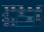
Arm Announces Next-Generation Neoverse V1 and N2 Cores

Ten years ago, Arm set its sights on deploying its compute-efficient technology in the data center with a vision towards a changing landscape that would require a new approach to infrastructure compute.

That decade-long effort to lay the groundwork for a more efficient infrastructure was realized when we announced Arm Neoverse, a new compute platform that would deliver 30% year-over-year performance improvements through 2021. The unveiling of our first two platforms, Neoverse N1 and E1, was significant and important. Not only because Neoverse N1 shattered our performance target by nearly 2x to deliver 60% more performance when compared to Arm's Cortex-A72 CPU, but because we were beginning to see real demand for more choice and flexibility in this rapidly evolving space.

SiFive To Introduce New RISC-V Processor Architecture and RISC-V PC at Linley Fall Virtual Processor Conference

SiFive, Inc., the leading provider of commercial RISC-V processor IP and silicon solutions, today announced that Dr. Yunsup Lee, CTO of SiFive, and Dr. Krste Asanovic, Chief Architect of SiFive, will present at the technology industry's premier processor conference, the Linley Fall Virtual Processor Conference. The conference will be held on October 20th - 22nd and 27th - 29th, 2020 and will feature high-quality technical content from leading semiconductor companies worldwide.

"Industry demand for AI performance has skyrocketed over the last few years driven by rapid adoption from the data center to the edge. This year's Linley Fall Processor Conference will feature our biggest program yet and will introduce a host of new technology disclosures and product announcements of innovative processor architectures and IP technologies," said Linley Gwennap, principal analyst and conference chairperson. "In spite of the challenges posed by the pandemic, development of these technologies continues to accelerate and we're excited to be sharing these presentations with a global audience via our live-streamed format."
Return to Keyword Browsing
May 8th, 2024 01:46 EDT change timezone

New Forum Posts

Popular Reviews

Controversial News Posts