News Posts matching #SoC

Return to Keyword Browsing

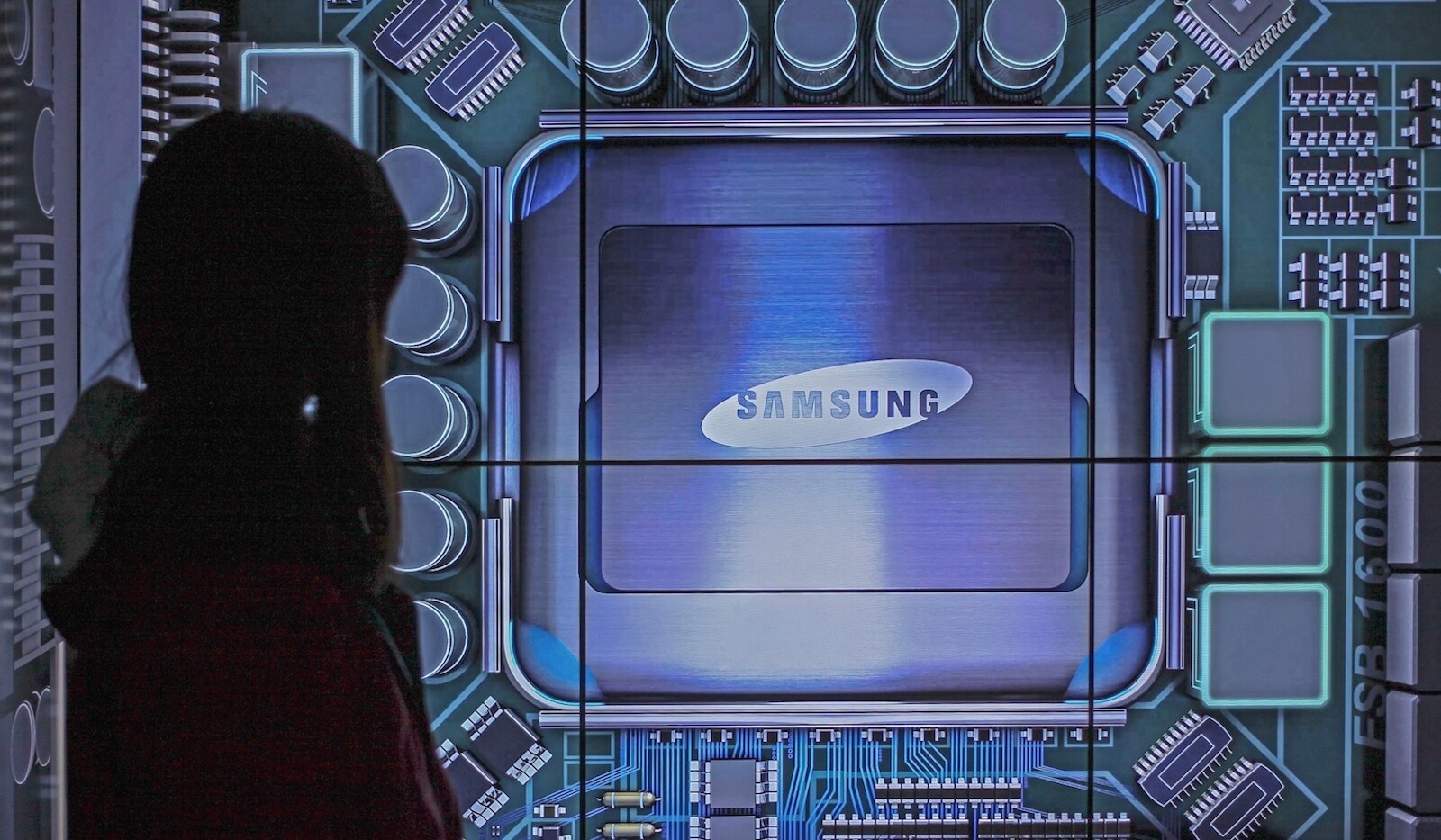
Samsung Prepares Mach-1 Chip to Rival NVIDIA in AI Inference

During its 55th annual shareholders' meeting, Samsung Electronics announced its entry into the AI processor market with the upcoming launch of its Mach-1 AI accelerator chips in early 2025. The South Korean tech giant revealed its plans to compete with established players like NVIDIA in the rapidly growing AI hardware sector. The Mach-1 generation of chips is an application-specific integrated circuit (ASIC) design equipped with LPDDR memory that is envisioned to excel in edge computing applications. While Samsung does not aim to directly rival NVIDIA's ultra-high-end AI solutions like the H100, B100, or B200, the company's strategy focuses on carving out a niche in the market by offering unique features and performance enhancements at the edge, where low power and efficient computing is what matters the most.

According to SeDaily, the Mach-1 chips boast a groundbreaking feature that significantly reduces memory bandwidth requirements for inference to approximately 0.125x compared to existing designs, which is an 87.5% reduction. This innovation could give Samsung a competitive edge in terms of efficiency and cost-effectiveness. As the demand for AI-powered devices and services continues to soar, Samsung's foray into the AI chip market is expected to intensify competition and drive innovation in the industry. While NVIDIA currently holds a dominant position, Samsung's cutting-edge technology and access to advanced semiconductor manufacturing nodes could make it a formidable contender. The Mach-1 has been field-verified on an FPGA, while the final design is currently going through a physical design for SoC, which includes placement, routing, and other layout optimizations.

NVIDIA "Blackwell" GeForce RTX to Feature Same 5nm-based TSMC 4N Foundry Node as GB100 AI GPU

Following Monday's blockbuster announcements of the "Blackwell" architecture and NVIDIA's B100, B200, and GB200 AI GPUs, all eyes are now on its client graphics derivatives, or the GeForce RTX GPUs that implement "Blackwell" as a graphics architecture. Leading the effort will be the new GB202 ASIC, a successor to the AD102 powering the current RTX 4090. This will be NVIDIA's biggest GPU with raster graphics and ray tracing capabilities. The GB202 is rumored to be followed by the GB203 in the premium segment, the GB205 a notch lower, and the GB206 further down the stack. Kopite7kimi, a reliable source with NVIDIA leaks, says that the GB202 silicon will be built on the same TSMC 4N foundry node as the GB100.

TSMC 4N is a derivative of the company's mainline N4P node, the "N" in 4N stands for NVIDIA. This is a nodelet that TSMC designed with optimization for NVIDIA SoCs. TSMC still considers the 4N as a derivative of the 5 nm EUV node. There is very little public information on the power- and transistor density improvements of the TSMC 4N over TSMC N5. For reference, the N4P, which TSMC regards as a 5 nm derivative, offers a 6% transistor-density improvement, and a 22% power efficiency improvement. In related news, Kopite7kimi says that with "Blackwell," NVIDIA is focusing on enlarging the L1 caches of the streaming multiprocessors (SM), which suggests a design focus on increasing the performance at an SM-level.

Sony PlayStation 5 Pro Details Emerge: Faster CPU, More System Bandwidth, and Better Audio

Sony is preparing to launch its next-generation PlayStation 5 Pro console in the Fall of 2024, right around the holidays. We previously covered a few graphics details about the console. However, today, we get more details about the CPU and the overall system, thanks to the exclusive information from Insider Gaming. Starting off, the sources indicate that PS5 Pro system memory will get a 28% bump in bandwidth, where the standard PS5 console had 448 GB/s, and the upgraded PS5 Pro will get 576 GB/s. Apparently, the memory system is more efficient, likely coming from an upgrade in memory from the GDDR6 SDRAM of the regular PS5. The next upgrade is the CPU, which has special modes for the main processor. The CPU uArch is likely the same, with clocks pushed to 3.85 GHz, resulting in a 10% frequency increase.

However, this is only achieved in the "High CPU Frequency Mode," which steals the SoC's power from the GPU and downclocks it slightly to allocate more power to the CPU in highly CPU-intense settings. The GPU we discussed here is an RDNA 3 IP with up to 45% faster graphics rendering. The ray tracing performance can be up to four times higher than the regular PS5, while the entire GPU delivers 33.5 TeraFLOPS of FP32 single-precision computing. This comes from 30 WGP running BVH8 shaders vs the 18 WGPs running BVH4 shaders on the regular PS5. There are PSSR upscalers present, and the GPU can output 8K resolution, which will come with future software updates. Last but not least, the AI front also has a custom AI accelerator capable of 300 8-bit INT8 TOPS and 67 16-bit FP16 TeraFLOPS. Audio codecs are getting some love, as well, with ACV running up to 35% faster.

Qualcomm Teases "Snapdragon 8s Gen 3" SoC Launch

Qualcomm's Weibo social media account has teased an upcoming new product launch: "the spring dragon raises its head, and everything is reborn! The new Snapdragon flagship is about to be released. Let's welcome the New Year and the new era. On March 18, please stay tuned for the Snapdragon flagship new product launch conference." News outlets believe that a variant of the current top-of-the-line Snapdragon 8 Gen 3 (SM8650-AB) chipset will be introduced next week. Smartphone tech tipster, Digital Chat Station, revealed that a mysterious Qualcomm Snapdragon "SM8635" model was in the pipeline. Early February speculation pointed to a possible "Snapdragon 8s Gen 3" moniker—the added "s" implies that this mobile processor could emerge as a cheaper "sub-flagship" model.

Geekbench 6.2.2 results—posted by a trio of Realme "RMX3851" android smartphones—revealed speculated "8s Gen 3" specifications, including a 3.01 GHz "Big" Core clock, an Adreno 735 integrated GPU, and a 1+3+4 cluster configuration. The pre-release samples could not keep up with finalized Snapdragon 8 Gen 3 hardware in performance gauntlets. A mid-range "Snapdragon 7+ Gen 3" SoC could make an appearance on March 18, but tipsters believe that the event will be dedicated to a single new product. Digital Chat Station reckons that Qualcomm will market the Snapdragon 8s Gen 3 "as a Little 8G3."

ScaleFlux SFX 5016 Will Set New Benchmarks for Enterprise SSD Efficiency and AI Workload Performance

As the IT sector continues to seek answers for scaling data processing performance while simultaneously improving efficiency - in terms of performance and density per watt, per system, per rack, and per dollar of CapEx and OpEx - ScaleFlux is answering the call with innovative design choices in its SSD controllers. The SFX 5016 promises to set new standards both for performance and for power efficiency.

In addition to carrying forward the transparent compression feature that ScaleFlux first released in 2020 in upgraded in 2022 with the SFX 3016 computational storage drive controller, the new SFX 5016 SOC processor includes a number of design advances.

Qualcomm Snapdragon X Elite Benchmarked Against Intel Core Ultra 7 155H

Qualcomm Snapdragon X Elite is about to make landfall in the ultraportable notebook segment, powering a new wave of Windows 11 devices powered by Arm, capable of running even legacy Windows applications. The Snapdragon X Elite SoC in particular has been designed to rival the Apple M3 chip powering the 2024 MacBook Air, and some of the "entry-level" variants of the 2023 MacBook Pros. These chips threaten the 15 W U-segment and even 28 W P-segment of x86-64 processors from Intel, such as the Core Ultra "Meteor Lake," and Ryzen 8040 "Hawk Point." Erdi Özüağ, prominent tech journalist from Türkiye, has access to a Qualcomm-reference notebook powered by the Snapdragon X Elite X1E80100 28 W SoC. He compared its performance to an off-the-shelf notebook powered by a 28 W Intel Core Ultra 7 155H "Meteor Lake" processor.

There are three tests that highlight the performance of the key components of the SoCs—CPU, iGPU, and NPU. A Microsoft Visual Studio code compile test sees the Snapdragon X Elite with its 12-core Oryon CPU finish the test in 37 seconds; compared to 54 seconds by the Core Ultra 7 155H with its 6P+8E+2LP CPU. In the 3DMark test, the Adreno 750 iGPU posts identical performance numbers to the Arc Graphics Xe-LPG of the 155H. Where the Snapdragon X Elite dominates the Intel chip is AI inferencing. The UL Procyon test sees the 45 TOPS NPU of the Snapdragon X Elite score 1720 points compared to 476 points by the 10 TOPS AI Boost NPU of the Core Ultra. The Intel machine is using OpenVINO, while the Snapdragon is using Qualcomm SNPE SDK for the test. Don't forget to check out the video review by Erdi Özüağ in the source link below.

Huawei's HiSilicon Taishan V120 Server Core Matches Zen 3 Performance

Huawei's new server CPU based on the HiSilicon Taishan V120 core has shown impressive single-threaded performance that matches AMD's Zen 3 architecture in a leaked Geekbench 6 benchmark. The Taishan V120 is likely being manufactured on SMIC's 7 nm process node. The Geekbench 6 result posted on social media does not identify the exact Huawei server CPU model, but speculation points to it being the upcoming Kunpeng 930 chip. In the benchmark, the Taishan V120 CPU operating at 2.9 GHz scored 1527 in the single-core test. This positions it nearly equal to AMD's EPYC 7413 server CPU based on the Zen 3 architecture, which boosts up to 3.6 GHz and which scored 1538 points. It also matches the single-threaded performance of Intel's Coffee Lake-based Xeon E-2136 from 2018, even though that Intel chip can reach 4.5 GHz boost speeds, scoring 1553 points.

The Taishan V120 core first appeared in Huawei's Kirin 9000 smartphone SoC in 2020. Using the core in server CPUs would allow Huawei to achieve competitive single-threaded performance to rival AMD's last-generation EPYC Milan and Intel's older Skylake server chips. Multi-threaded benchmarks will be required to gauge the Kunpeng 930's overall performance fully when it launches. Huawei continues innovating its ARM-based server CPU designs even while facing restrictions on manufacturing and selling chips internationally due to its inclusion on the US Entity List in 2019. The impressive single-threaded results versus leading x86 competitors demonstrate Huawei's resilience and self-reliance in developing homegrown data center technology through its HiSilicon division. More details on the Kunpeng 930 server chip will likely surface later this year, along with server configurations from Chinese OEMs.

Qualcomm "Snapdragon 8s Gen 3" SoC with Adreno 735 GPU Gets Geekbenched

A mysterious Qualcomm Snapdragon "SM8635" model emerged earlier this month—courtesy of ever reliable smartphone tech tipster Digital Chat Station. They claimed that the unnamed mobile chipset had posted an AnTuTu score of roughly 1.7 million, with specifications including one Cortex-X4 core clocked at 2.9 GHz and an integrated Adreno 735 GPU. TSMC's 4 nm process node was also mentioned—not a particularly big revelation since the latest Snapdragon flagship is a 4 nm part. Early guess work pointed to possible Snapdragon 8s Gen 2 or Snapdragon 8 Gen 3 Lite guises, but a Geekbench Browser leak indicates that SM8635 is destined to become "Snapdragon 8s Gen 3," in Digital Chat Station's opinion.

A Realme "RMX3851" android device was tested in Geekbench 6.2.2—stated specifications include a 3.01 GHz "Big" Core clock, Adreno 735 GPU, and a 1+3+4 cluster configuration. Many believe that the SM8635 is positioned as a cut-down alternative to Snapdragon 8 Gen 3 (SM8650-AB), given that Realme specializes in producing value-oriented "near flagship" specced smartphones. Wccftech has spent hands-on time with various Qualcomm Snapdragon 8 Gen 3-powered devices: "You can see in (Realme's Geekbench entry) that the alleged Snapdragon 8s Gen 3 does not perform on the same level as its elder brother, which scores higher in both single and multi-core. For the sake of reference, I have seen the elder sibling going as high as 2,329 in single-core tests and 7,501 in multi-core tests. So, this chipset is performing at half the speed, but of course, this seems like a device that is not completely ready, so the final scores might improve." Further (insider) leaks or an official Qualcomm announcement will confirm whether the posited "Snapdragon 8s Gen 3" moniker is a good guess, although another leaked chip suggests another path. Roland Quandt reckons that a similarly configured "SM7675" SoC will be joining the Snapdragon 7 Gen family.

Intel to Make its Most Advanced Foundry Nodes Available even to AMD, NVIDIA, and Qualcomm

Intel CEO Pat Gelsinger, speaking at the Intel Foundry Services (IFS) Direct Connect event, confirmed to Tom's Hardware that he hopes to turn IFS into the West's premier foundry company, and a direct technological and volume rival to TSMC. He said that there is a clear line of distinction between Intel Products and Intel Foundry, and that later this year, IFS will be more legally distinct from Intel, becoming its own entity. The only way Gelsinger sees IFS being competitive to TSMC, is by making its most advanced semiconductor manufacturing nodes and 3D chip packaging innovations available to foundry customers other than itself (Intel Products), even if it means providing them to companies that directly compete with Intel products, such as AMD and Qualcomm.

Paul Alcorn of Tom's Hardware asked CEO Gelsinger "Intel will now offer its process nodes to some of its competitors, and there may be situations wherein your product teams are competing directly with competitors that are enabled by your crown jewels. How do you plan to navigate those types of situations and maybe soothe ruffled feathers on your product teams?" To this, Gelsinger responded "Well, if you go back to the picture I showed today, Paul, there are Intel products and Intel foundry, There's a clean line between those, and as I said on the last earnings call, we'll have a setup separate legal entity for Intel foundry this year," Gelsinger responded. "We'll start posting separate financials associated with that going forward. And the foundry team's objective is simple: Fill. The. Fabs. Deliver to the broadest set of customers on the planet."

Cadence Digital and Custom/Analog Flows Certified for Latest Intel 18A Process Technology

Cadence's digital and custom/analog flows are certified on the Intel 18A process technology. Cadence design IP supports this node from Intel Foundry, and the corresponding process design kits (PDKs) are delivered to accelerate the development of a wide variety of low-power consumer, high-performance computing (HPC), AI and mobile computing designs. Customers can now begin using the production-ready Cadence design flows and design IP to achieve design goals and speed up time to market.

"Intel Foundry is very excited to expand our partnership with Cadence to enable key markets for the leading-edge Intel 18A process technology," said Rahul Goyal, Vice President and General Manager, Product and Design Ecosystem, Intel Foundry. "We will leverage Cadence's world-class portfolio of IP, AI design technologies, and advanced packaging solutions to enable high-volume, high-performance, and power-efficient SoCs in Intel Foundry's most advanced process technology. Cadence is an indispensable partner supporting our IDM2.0 strategy and the Intel Foundry ecosystem."

Intel Announces Intel 14A (1.4 nm) and Intel 3T Foundry Nodes, Launches World's First Systems Foundry Designed for the AI Era

Intel Corp. today launched Intel Foundry as a more sustainable systems foundry business designed for the AI era and announced an expanded process roadmap designed to establish leadership into the latter part of this decade. The company also highlighted customer momentum and support from ecosystem partners - including Synopsys, Cadence, Siemens and Ansys - who outlined their readiness to accelerate Intel Foundry customers' chip designs with tools, design flows and IP portfolios validated for Intel's advanced packaging and Intel 18A process technologies.

The announcements were made at Intel's first foundry event, Intel Foundry Direct Connect, where the company gathered customers, ecosystem companies and leaders from across the industry. Among the participants and speakers were U.S. Secretary of Commerce Gina Raimondo, Arm CEO Rene Haas, Microsoft CEO Satya Nadella, OpenAI CEO Sam Altman and others.

Alleged ARM Cortex-X5 Underperformance Linked to Power Consumption Concerns

ARM's in-progress fifth generation "Blackhawk" Cortex design is allegedly going through a troubled phase of development, according to Chinese insider sources. A Revegnus (@Tech_Reve) social media post highlights ongoing issues: "It's reported that the Cortex X5 architecture is underperforming compared to expectations. It's speculated that the high-frequency power consumption has surged explosively. Therefore, if performance is reduced for lower power consumption, the Geekbench 6 multi-core score of Dimensity 9400 may not achieve a score of 9,400 points." A recent Moor Insights & Strategy analysis piece proposed that "Blackhawk" would become "the most powerful option available at launch" later this year—mobile chipsets leveraging ARM's Cortex-X5 design are touted to face tough next-gen competition from Qualcomm and Apple corners.

Revegnus pulled in a rival SoC: "While Snapdragon 8 Gen 4 is seen to have minor issues, there is no evidence to support this claim. There might be a problem with low-frequency power consumption not showing clear superiority over ARM's middle cores." Qualcomm's next flagship model is performing admirably according to insiders—an engineering sample managed to score 10,628 points in alleged Geekbench 6 multi-core gauntlets. Late last month prototype clocks were leaked—Digital Chat Station claimed that a Snapdragon 8 Gen 4 High-Performance "Big" core was capable of reaching 4.0 GHz. Prior to the latest news, MediaTek's Dimensity 9400 SoC was observed achieving ~10,000 multi-core Geekbench 6 scores—leaked CPU cluster details present a single "Big" Cortex-X5 unit operating alongside three Cortex-X4 cores.

Games Consultant Predicts H2Y24 Launch for PlayStation 5 Pro

Serkan Toto, CEO of Tokyo-based games consultancy Kantan Games was interviewed by CNBC earlier this week—he was invited on-air to provide expert commentary on Sony's freshly revised sales and revenue forecast for PlayStation 5 products. He believes that great forward momentum is best achieved with refreshed hardware, and a well timed launch coinciding with the release of AAA/blockbuster games titles. Last autumn's rollout of slimmer PlayStation 5 consoles was not particularly exciting—with no major bump up in specs or attractive pricing. The development of an inevitable "Pro" variant has circulated around rumor mills for more than a year.

Sony Computer Entertainment (SCE) and AMD are believed to co-operating on a very potent hardware redesign—reports from late last year posited that a semi-custom "Viola" SoC is in the pipeline. A more expensive RDNA 3-upgraded refresh could attract an additional segment of hardcore gamers, but another industry analyst reckons that Sony is unlikely to implement a standard model price cut later this year (based on past trends). George Jijiashvili, senior principal analyst at Omdia, stated: "A scenario where Sony launches a PS5 Pro, but still experiences declining year-on-year hardware sales is very much within the realms of possibility." Serkan Toto (of Kantan Games consultancy) expressed a more optimistic view: "There seems to be a broad consensus in the game industry that Sony is indeed preparing a launch of a PS5 Pro in the second half of 2024...And Sony will want to make sure to have a great piece of hardware ready when GTA VI hits in 2025, a launch that will be a shot in the arm for the entire gaming industry."

Intel Foundry Services (IFS) and Cadence Design Systems Expand Partnership on SoC Design

Intel Foundry Services (IFS) and Cadence Design Systems Inc. today announced a multiyear strategic agreement to jointly develop a portfolio of key customized intellectual property (IP), optimized design flows and techniques for Intel 18A process technology featuring RibbonFET gate-all-around transistors and PowerVia backside power delivery. Joint customers of the companies will be able to accelerate system-on-chip (SoC) project schedules on process nodes from Intel 18A and beyond while optimizing for performance, power, area, bandwidth and latency for demanding artificial intelligence, high performance computing and premium mobile applications.

"We're very excited to expand our partnership with Cadence to grow the IP ecosystem for IFS and provide choice for customers," said Stuart Paann, Intel senior vice president and general manager of IFS. "We will leverage Cadence's world-class portfolio of leading IP and advanced design solutions to enable our customers to deliver high-volume, high-performance and power-efficient SoCs on Intel's leading-edge process technologies."

Intel Lunar Lake A1 Sample CPU Boost & Cache Specs Leak Out

HXL (@9550pro) has highlighted an intriguing pinned post on the Chinese Zhihu community site—where XZiar, a self described "Central Processing Unit (CPU) expert," has shared a very fuzzy/low quality screenshot of a Windows Task Manager session. The information on display indicates that a "Genuine Intel(R) 0000 1.0 GHz" processor was in use—perhaps a very early Lunar Lake (LNL) engineering sample (ES1). XZiar confirmed the pre-release nature of the onboard chip, and teased its performance prowess: "It's good to use the craftsmanship that others have stepped on. It can run 2.8 GHz with only A1 step, and it is very smooth."

The "A1" designation implies that the leaked sample is among the first LNL processor prototypes to exit manufacturing facilities—Intel previewed its "Lunar Lake-MX" SoC package to press representatives last November. XZiar's followers have pored over the screenshot and ascertained that the leaked example sports a "8-core + 8-thread, without Hyperthreading, 4P+4LPE" configuration. Others were confused by the chip's somewhat odd on-board cache designations—L1: 836 KB, L2: 14 MB and L3: 12 MB—XZiar believes that prototype's setup "is obviously not up to par," when a replier compares the spec to an N300 series processor. It is theorized that Windows Task Manager is simply not fully capable of detecting the sample's full makeup, but XZiar reckons that 12 MB of L3 cache is the correct figure.

Nintendo Switch 2 Could Retain Backward Compatibility with The First-Gen Console

Reports are circulating online that Nintendo's upcoming successor to the Switch console, tentatively referred to as the "Switch 2," will offer backward compatibility for physical game cards and digital purchases from the current Switch library. While Nintendo has yet to officially announce the new console, speculation points to a potential reveal as early as next month for a 2024 launch. The backward compatibility claims first surfaced last year when Nintendo America President Doug Bowser hinted at supporting continuity between console generations to minimize the sales decline when transitioning hardware. New momentum behind the rumors comes from gaming industry insiders Felipe Lima and PH Brazil, who, during recent podcasts, stated the Switch 2 has backward compatibility functionality already being shared with game developers.

Well-known gaming leakers "NateTheHate" and others have corroborated that testing is underway for playing current Switch games on new hardware. If true, this backward compatibility would be a consumer-friendly move that breaks from Nintendo's past tendencies of forcing clean breaks between console ecosystems. While details remain unconfirmed by Nintendo, multiple credible sources point to the upcoming Switch successor allowing gamers to carry forward both their physical and digital libraries to continue enjoying this generation's releases. If the compatibility remains, the hardware platform could stay in the playing field of the same vendor—NVIDIA—who provided Nintendo with Tegra X1 SoC. The updated version of the SoC could use a fork of NVIDIA's Orin platform based on Ampere GPU with DLSS, but official details are yet to be seen.

iFixit Teardown Guide Puts Spotlight on Apple Vision Pro Logic Board

iFixit has finally posted photos of the Apple Vision Pro's inner bits, following on from the release of a video teardown (uploaded last week)—the American e-commerce and how-to website spent plenty of hours exploring the expensive mixed reality headset's "creepy" features, before breaking seals and deconstructing the device's highly complex interior. The iFixit teardown team have often complained about Apple computer products being notoriously difficult to deal with—the Vision Pro is no exception, but they eventually managed to isolate the headset's logic board. The onboard M2 octa-core chipset is identified as a APL1109/339S01081E part, while its assistant R1 sensor co-processor sports an APL1W08/339S01186 identifier. Micron has supplied 8 GB of LPDDR5 SDRAM memory (MT62F1G64D8WT-031 XT), and Kioxia has Apple covered with its K5A4RC2097 256 GB NAND flash.

Tech experts have spent time poring over iFixit's latest set of snaps, as laid out in their teardown guide—one such enthusiast, Yining Karl Li, posted an intriguing Apple Vision Pro Logic Board observation to social media: "There's this interesting shot of the main logic board (in Step 1). The R1 chip (in the red box) has interesting lines all over it dividing the surface into sub-boxes. Is the R1 chip using a chiplet design?" A small debate erupted from this quick inspection—one commenter believes that the co-processor is not all that fancy: "(it is) likely sporting low-latency fan-out memory," citing the presence of very faint horizontal and vertical lines. As pointed out by Wccftech, Li also presented a chiplet design example (for comparison purposes)—a close-up shot of Intel's Ponte Vecchio Xe-HPC GPU. The lines are a lot more pronounced on Team Blue's chip design.

AMD Unveils Embedded+ Architecture, Combining Embedded Processors with Adaptive SoCs

AMD today announced the launch of AMD Embedded+, a new architectural solution that combines AMD Ryzen Embedded processors with Versal adaptive SoCs onto a single integrated board to deliver scalable and power-efficient solutions that accelerate time-to-market for original design manufacturer (ODM) partners. Validated by AMD, the Embedded+ integrated compute platform helps ODM customers reduce qualification and build times for faster time-to-market without needing to expend additional hardware and R&D resources. ODM integration using Embedded+ architecture enables the use of a common software platform to develop designs with low power, small form factors, and long lifecycles for medical, industrial, and automotive applications.

"In automated systems, sensor data has diminishing value with time and must operate on the freshest information possible to enable the lowest latency, deterministic response," said Chetan Khona, senior director of Industrial, Vision, Healthcare and Sciences Markets, AMD. "In industrial and medical applications, many decisions need to happen in milliseconds. Embedded+ maximizes the value of partner and customer data, with energy efficiency and performant computing that enables them to focus in turn on addressing their customer and market needs."

SMIC Reportedly Ramping Up 5 Nanometer Production Line in Shanghai

Semiconductor Manufacturing International Corp (SMIC) is preparing new semiconductor production lines at its Shanghai facilities according to a fresh Reuters report—China's largest contract chip maker is linked to next generation Huawei SoC designs, possibly 5 nm-based Kirin models. SMIC's newest Shanghai wafer fabrication site was an expensive endeavor—involving a $8.8 billion investment—but their flagship lines face a very challenging scenario with new phases of mass production. Huawei, a key customer, is expected to "upgrade" to a 5 nm process for new chip designs—their current flagship, Kirin 9000S, is based on a SMIC 7 nm node. Reuter's industry sources believe that the foundry's current stable of "U.S. and Dutch-made equipment" will be deployed to "produce 5-nanometer chips."

Revised trade rulings have prevented ASML shipping advanced DUV machinery to mainland China manufacturing sites—SMIC workers have reportedly already repurposed the existing inventory of lithography equipment for next-gen pursuits. Burn Lin (ex-TSMC), a renowned "chip guru," believes that it is possible to mass produce 5 nm product on slightly antiquated gear (previously used for 7 nm)—but the main caveats being increased expense and low yields. According to a DigiTimes Asia report, mass production of a 5 nm SoC on SMIC's existing DUV lithography would require four-fold patterning in a best case scenario.

Intel, Microsoft, and Cirrus Logic Collaborate on Lunar Lake Reference Laptop Design

Intel, Microsoft, and a fabless semiconductor company making analog, mixed-signal, and audio DSP, Cirrus Logic, have collaborated on a new reference laptop design to showcase the upcoming Lunar Lake mobile CPUs. The goal is to enable "cool, quiet, and high-performance" laptops that push the boundaries of efficiency, thickness, and acoustics. The reference design incorporates three key components from Cirrus Logic - the CP9314 power converter chip, CS42L43 audio codec, and CS35L56 amplifier. The CP9314 is the most critical element, using advanced power conversion technology to improve Lunar Lake's power efficiency significantly. This enables thinner and quieter laptops with longer battery life. The codec and amplifier chips also play a role, providing high-quality audio with next-generation features like spatial audio support.

Together, these Cirrus Logic components aim to highlight Lunar Lake's capabilities for efficiency, performance, and immersive experiences in a thin and light form factor. While details remain scarce on the Lunar Lake CPUs themselves, they are expected to arrive later this year, likely in the second half. If the reference laptops live up to their promises, Lunar Lake could help Intel regain leadership in mobile computing efficiency, which has been lacking since the introduction of Apple's M series SoCs, which have superior battery life. With expert collaboration from Microsoft and Cirrus Logic on the peripheral hardware and software, Lunar Lake may usher in a new generation of cool, quiet, and powerful laptops.

Intel Foundry Services Get 18A Order: Arm-based 64-Core Neoverse SoC

Faraday Technology Corporation, a Taiwanese silicon IP designer, has announced plans to develop a new 64-core system-on-chip (SoC) utilizing Intel's most advanced 18A process technology. The Arm-based SoC will integrate Arm Neoverse compute subsystems (CSS) to deliver high performance and efficiency for data centers, infrastructure edge, and 5G networks. This collaboration brings together Faraday, Arm, and Intel Foundry Services. Faraday will leverage its ASIC design and IP solutions expertise to build the SoC. Arm will provide the Neoverse compute subsystem IP to enable scalable computing. Intel Foundry Services will manufacture the chip using its cutting-edge 18A process, which delivers one of the best-in-class transistor performance.

The new 64-core SoC will be a key component of Faraday's upcoming SoC evaluation platform. This platform aims to accelerate customer development of data center servers, high-performance computing ASICs, and custom SoCs. The platform will also incorporate interface IPs from the Arm Total Design ecosystem for complete implementation and verification. Both Arm and Intel Foundry Services expressed excitement about working with Faraday on this advanced Arm-based custom silicon project. "We're thrilled to see industry leaders like Faraday and Intel on the cutting edge of Arm-based custom silicon development," said an Arm spokesperson. Intel SVP Stuart Pann said, "We are pleased to work with Faraday in the development of the SoC based on Arm Neoverse CSS utilizing our most competitive Intel 18A process technology." The collaboration represents Faraday's strategic focus on leading-edge technologies to meet evolving application requirements. With its extensive silicon IP portfolio and design capabilities, Faraday wants to deliver innovative solutions and break into next-generation computing design.

Qualcomm & Samsung Sign Extended Multi-year Snapdragon Deal

Cristiano Renno Amon, President and CEO of Qualcomm, discussed the successful launch of his company's Snapdragon 8 Gen 3 mobile platform during a January 31 Earnings Call—expectations have been set high for the flagship smartphone chipset: "(bringing) a new standard for on-device gen AI experiences for premium smartphones and powers all through flagship Android devices launched and launching this fiscal year." Amon highlighted Samsung's recently rolled out Galaxy S24 Ultra range, that makes use of a special "For Galaxy" Snapdragon 8 Gen 3 SoC. Industry watchdogs have continued to question Samsung's reliance on third-party processor solutions (including MediaTek Dimensity parts), despite having access to plenty of "worthy" in-house technology. Their flagship Exynos 2400 chip has been deployed with the Galaxy S24 Plus range, but Qualcomm Snapdragon-equipped devices offer better performance and efficiency.

The picky segment of Samsung's smartphone userbase will be pleased to hear about a renewed agreement between it and Qualcomm, which includes a trickling down to mid-range offerings—Amon made a big announcement during the late January conference call: "We're also announcing that we extended a multi-year agreement with Samsung relating to Snapdragon platforms for flagship Galaxy smartphone launches starting in 2024. The extended agreement demonstrates the value of Snapdragon 8, our technology leadership and our successful long-term strategic partnership with Samsung. In the quarter, we also announced the Snapdragon 7 Gen 3 mobile platform, which brings leading gen AI capabilities to high-tier Android smartphones and is a category leader in both experiences and performance." Going forward, Samsung is likely sticking with its current operating model of peppering a mix of Snapdragon and Exynos chipsets throughout its Galaxy Z, S and A product ranges.

Snapdragon 8 Gen 4 Touted for Mass Production in Q3Y24

Qualcomm and its smartphone manufacturer partners are reported to be in a rush to get the Snapdragon 8 Gen 4 chipset released later this year—Digital Chat Station believes that a pioneering mobile device could enter a mass production phase around September of this year. Prototype devices are allegedly up and running—the tipster's insider sources have alluded to engineering samples being capable of reaching 4.0 GHz clocks on a high-powered Big Core (Nuvia's Oryon or Phoenix). Qualcomm's Snapdragon 8 Gen 3 SoC was revealed last October, and working hardware is slowly trickling out via retail avenues in early 2024—Digital Chat Station does not provide any reasoning behind the race to get the successor across the finish line within the same year.

An unnamed smartphone manufacturer is said to have outfitted a "dual-curved screen" model with a Snapdragon 8 Gen 4 chipset—Wccftech's report suggests that Xiaomi usually gets first dibs on cutting edge Qualcomm processor tech. The Nuvia engineering team has likely got their custom Oryon cores running to more than satisfactory levels—the article points out that: "a previous Geekbench 6 single-core and multi-core leak revealed that the (3 nm) Snapdragon 8 Gen 4 competes with Apple's M3 and is 46 percent faster than the Snapdragon 8 Gen 3 in multi-threaded workloads." Qualcomm is facing fierce flagship chip competition in 2024—MediaTek's Dimensity 9400 SoC could arrive at a cheaper price point, while offering comparable performance and efficiency.

Snapdragon 8 Gen 4's High Performance Core Allegedly Hitting 4.0 GHz

Digital Chat Station has seemingly received insider information regarding the performance of Qualcomm's Snapdragon 8 Gen 4 mobile chipset—their source reports that a probable engineering sample is already exceeding its predecessor's Big core (Cortex-X4) maximum limit of 3.3 GHz. The rumor mill has Nuvia's custom Oryon cores linked to the next generation mobile processor, although some experts think that the Phoenix design was selected for Gen 4. Qualcomm's Snapdragon X Elite notebook SoC was unveiled last October—this ARM-based solution is set to deliver "a dramatic leap in innovation for computing" thanks to Nuvia's custom Oryon technology. Kedar Kondap, Senior Vice President & General Manager of Compute & Gaming stated that the Snapdragon X Elite offers: "super-charged performance that will delight consumers with incredible power efficiency and take their creativity and productivity to the next level."

Digital Chat Station's brief assessment of the prototype Snapdragon 8 Gen 4's Big core prowess is also glowing: "4.0 GHz is no longer a dream" on smartphones. Past reports have Qualcomm signed up with TSMC for an unspecified 3 nm production process—next generation silicon will benefit greatly in terms of power efficiency, with custom Oryon or Phoenix cores (allegedly) achieving greater clock speeds thanks to some extra headroom. As mentioned above, the previous-gen Kryo Prime core—using TSMC's advanced 4 nm node—is factory restricted to 3.3 GHz. Tipsters reckon that efficiency cores are not part of the Snapdragon 8 Gen 4 design, due to the innate benefits of 3 nm—according to Digital Chat Station, MediaTek is taking similar steps with its upcoming Dimensity 9400 SoC.

ARM Confirms Existence of Next-gen Cortex-X "Blackhawk" Unit

Last week Patrick Moorhead, CEO and founder of Moor Insights & Strategy, shared his insider sourced thoughts about ARM's next generation Cortex-X processor: "Blackhawk is planned to enable in smartphones shipping at the end of 2024. I think phones could be on the shelf a year from now at CES or maybe MWC." Moorhead believes that Cortex-X4's successor will be the most powerful option available at launch, which forms part of (ARM CEO) Rene Haas's strategy to "eliminate the performance gap between ARM-designed processors and custom ARM implementations." He believes that "this is a big and bold claim," since Apple is widely considered to rule the roost here with its cutting edge ARM-based Bionic designs. Moorhead's inside information has "Blackhawk" demonstrating the "largest year-over-year IPC performance increase in 5 years" citing undisclosed Geekbench 6 results.

He also presented evidence that the artificial intelligence processing is a key focus: "I am hopeful these performance goals translate to app performance as well. ARM also believes that Blackhawk will provide "great" LLM performance. I will assume that this has to do with big CPU IPC performance improvements as ARM says that its Cortex CPU is the #1 AI target for developers...The NPU and GPU can be an efficient way to run AI, but a CPU is the easiest and most pervasive way, which is why developers target it. A higher-performing CPU obviously helps here, but as the world moves increasingly to smaller language models, Arm's platform with higher-performing CPU and GPU combined with its tightly integrated ML libraries and frameworks will likely result in a more efficient experience on devices."

Return to Keyword Browsing
Jun 27th, 2025 06:06 CDT change timezone

New Forum Posts

Popular Reviews

TPU on YouTube

Controversial News Posts