Saturday, February 17th 2024

Intel Lunar Lake A1 Sample CPU Boost & Cache Specs Leak Out

HXL (@9550pro) has highlighted an intriguing pinned post on the Chinese Zhihu community site—where XZiar, a self described "Central Processing Unit (CPU) expert," has shared a very fuzzy/low quality screenshot of a Windows Task Manager session. The information on display indicates that a "Genuine Intel(R) 0000 1.0 GHz" processor was in use—perhaps a very early Lunar Lake (LNL) engineering sample (ES1). XZiar confirmed the pre-release nature of the onboard chip, and teased its performance prowess: "It's good to use the craftsmanship that others have stepped on. It can run 2.8 GHz with only A1 step, and it is very smooth."

The "A1" designation implies that the leaked sample is among the first LNL processor prototypes to exit manufacturing facilities—Intel previewed its "Lunar Lake-MX" SoC package to press representatives last November. XZiar's followers have pored over the screenshot and ascertained that the leaked example sports a "8-core + 8-thread, without Hyperthreading, 4P+4LPE" configuration. Others were confused by the chip's somewhat odd on-board cache designations—L1: 836 KB, L2: 14 MB and L3: 12 MB—XZiar believes that prototype's setup "is obviously not up to par," when a replier compares the spec to an N300 series processor. It is theorized that Windows Task Manager is simply not fully capable of detecting the sample's full makeup, but XZiar reckons that 12 MB of L3 cache is the correct figure.

A Tom's Hardware article has similarly analyzed the A1 chip's screenshot credentials—they have compiled this data into a speculative specification sheet (see above). They noted a couple of differences—when compared to Intel's current mobile CPU generation: "The L1 cache designation implies that Lunar Lake doesn't come with any low-power E-Cores like Meteor Lake, or all are low-power but with increased L1 cache size. The 2.8 GHz boost clock is also unsurprising since the sample is likely ES silicon...Things get weird when you start looking at the cache, though. It would appear Lunar Lake is identical to Meteor Lake in the L1 and L2 cache, or at least that's what the screenshot implies. However, the Lunar Lake sample has only 12 MB of L3 cache, lower than the 14 MB of L2 cache. Usually, a higher level of cache means more capacity, and often significantly more, so it's very unintuitive that Lunar Lake should have less L3 than L2 cache. This directly contradicts an earlier leak that showed 16 MB of L3 cache for Lunar Lake but has identical specifications otherwise."

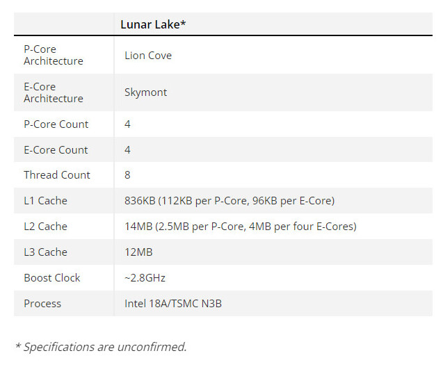
They also took issue with the sample's alleged thread count (just eight): "Intel's previous hybrid architecture CPUs have included Hyper-Threading for the P-Cores, which should result in 12 threads. Since A1 silicon is unlikely to be the final product, it's possible it's simply disabled because of technical issues or for testing purposes. On the other hand, early Arrow Lake samples don't have Hyper-Threading either. Although that could be a coincidence, it raises the possibility that Intel may be moving on from Hyper-Threading in 2024."
Sources: Zhihu, HXL Tweet, Tom's Hardware, Guru3D (image source)
Add your own comment

20 Comments on Intel Lunar Lake A1 Sample CPU Boost & Cache Specs Leak Out

#1
kondamin
That is quite a bit of silicon for a consumer grade chip tile thing
Posted on Reply
#2
Shou Miko
I really have it performance better than the current U sku's in laptops with only 2 p-cores they are not worth my time when I do support for office work it takes me double the time to fix the basics compared to i5-1135G7 sadly.
Posted on Reply
#3
Dirt Chip
Hoping it take less than 400W to run...
Posted on Reply
#4
InVasMani
Removing HT to me seems rather weird if true. Decompression benefits from more threading. I'd actually expect them to expand the amount of HT per P core if anything. The other thing I'd have expected is doing shared cache on P cores like is done with E cores because in some scenario's it would help bump up IPC if a P core has access to more L cache all it once. It wouldn't help in all scenario's, but in some of them it should provide uplift. It better be a net gain in the end of true and done with good reason otherwise they shot themselves in the foot and are teetering on a Bulldozer level of blunder. Bulldozer was actually good in a very select few sets of oddball scenario's though in spite of being a overall fiasco and catastrophic failure of a architecture as a whole and at the wrong moment for AMD having somewhat grossly overpaid for ATI at the time much more than it was really valued at.
Posted on Reply
#5
Jim Hutchinson
Dirt ChipHoping it take less than 400W to run...
Lunar Lake is targeting the low-power laptop section, so probably sub 40W let alone 400W. We'll need to see Arrow Lake for the high-power stuff.
Posted on Reply
#6
kondamin
InVasManiRemoving HT to me seems rather weird if true. Decompression benefits from more threading. I'd actually expect them to expand the amount of HT per P core if anything. The other thing I'd have expected is doing shared cache on P cores like is done with E cores because in some scenario's it would help bump up IPC if a P core has access to more L cache all it once. It wouldn't help in all scenario's, but in some of them it should provide uplift. It better be a net gain in the end of true and done with good reason otherwise they shot themselves in the foot and are teetering on a Bulldozer level of blunder. Bulldozer was actually good in a very select few sets of oddball scenario's though in spite of being a overall fiasco and catastrophic failure of a architecture as a whole and at the wrong moment for AMD having somewhat grossly overpaid for ATI at the time much more than it was really valued at.
I doubt intel is going to do much brand new other than their tiles and their new AVX scheme until they have 7nm running as it should.
Posted on Reply
#7
Vayra86
Hey look! Another Intel quad core :P
Posted on Reply
#8
efikkan
T0@stThe L1 cache designation implies that Lunar Lake doesn't come with any low-power E-Cores like Meteor Lake, or all are low-power but with increased L1 cache size. The 2.8 GHz boost clock is also unsurprising since the sample is likely ES silicon...Things get weird when you start looking at the cache, though. It would appear Lunar Lake is identical to Meteor Lake in the L1 and L2 cache, or at least that's what the screenshot implies. However, the Lunar Lake sample has only 12 MB of L3 cache, lower than the 14 MB of L2 cache. Usually, a higher level of cache means more capacity, and often significantly more, so it's very unintuitive that Lunar Lake should have less L3 than L2 cache.
While it usually is, it doesn't really matter from the core's perspective, as a core only sees its own L1 and L2*, and the whole L3. Adding up the total L1 and L2 is simply not useful or even relevant information, as these are separate caches, and it really tells us that whoever views L1 and L2 that way doesn't understand caches. I often chuckle when I see this (incl. the Windows task manager).
(*E-cores are different)

As for accuracy of the specifications, the Windows API probably gets this information from the CPUID instruction, which can be programmed in firmware to report misinformation (intentionally, not to reveal the true specifications of ES). And this could be a lower tier bin, or a chip with some L3 disabled for some reason.

Or there is the very possible scenario where this new generation is so significantly more efficient so it doesn't need so much L3. L3 works very differently from L2, and is a spillover cache for all the cores. If a new microarchitecture happens to be significantly more accurate in branch prediction, misprediction recovery and fetching of data/instructions, it could easily end up having a much less "efficient" L3, meaning the transistors could be better spent elsewhere. I've long been skeptical about this large L3 gimmick in recent years, as it generally does little for overall performance, and mostly helps software with fairly low computational density (bloated). While everything that "helps" is ultimately good, I'd prefer the R&D and transistor budget being spent on actually making faster architectures.
Posted on Reply
#9
PrettyKitten800
Databasedgod
InVasManiRemoving HT to me seems rather weird if true. Decompression benefits from more threading. I'd actually expect them to expand the amount of HT per P core if anything. The other thing I'd have expected is doing shared cache on P cores like is done with E cores because in some scenario's it would help bump up IPC if a P core has access to more L cache all it once. It wouldn't help in all scenario's, but in some of them it should provide uplift. It better be a net gain in the end of true and done with good reason otherwise they shot themselves in the foot and are teetering on a Bulldozer level of blunder. Bulldozer was actually good in a very select few sets of oddball scenario's though in spite of being a overall fiasco and catastrophic failure of a architecture as a whole and at the wrong moment for AMD having somewhat grossly overpaid for ATI at the time much more than it was really valued at.
HyperThreading and SMT will both be phased out eventually. It's a workaround from 20 years ago and its simply not as effective as having more, smaller cores. Intel themselves have already proved this with their E cores. Every single non-x86 cpu doesn't use HT/SMT because it was never efficient enough to cut it in the handheld market, where efficiency gains mean performance gains. Designers have noticed this and begun applying the same logic to larger systems. Just look at the performance/watt of Apple M chips compared to their Intel and AMD counterparts. AMD is even using the same process node as Apple, but it still isn't competitive in this aspect. GPUs are also a great example. They have been multicore from the very start and no GPU design has ever incorporated HT/SMT.
Posted on Reply
#10
Wirko
InVasManiThe other thing I'd have expected is doing shared cache on P cores like is done with E cores because in some scenario's it would help bump up IPC if a P core has access to more L cache all it once.
You mean L2? But shared L2 would also mean shared access to ring bus - that's almost certain, if not strictly necessary. And that wouldn't be good.
PrettyKitten800HyperThreading and SMT will both be phased out eventually. It's a workaround from 20 years ago and its simply not as effective as having more, smaller cores.
I can't say I agree but SMT must be a scheduling nightmare of the same magnitude as P+E cores. Deciding which pairs of software threads are good candidates for running on the same core is not at all simple, but is crucial for performance.
But then you've also got those "clusters" of E's. Ugh. Deciding which software threads are good candidates for running on the same cluster, with shared L2 and bus stop, is also something that can potentially be done very wrong. How did Intel even get away with their way of counting cores, but AMD with their Bulldozer didn't?
Posted on Reply
#11
pressing on
kondaminThat is quite a bit of silicon for a consumer grade chip tile thing
Some sources claim that the chip pictured is not a Lunar Lake CPU. But could be a Meteor Lake based prototype featuring on-package LPDDR5X memory that was used as a stand-in.
Posted on Reply
#12
kondamin
pressing onSome sources claim that the chip pictured is not a Lunar Lake CPU. But could be a Meteor Lake based prototype featuring on-package LPDDR5X memory that was used as a stand-in.
Possible, even still if that is how big it is going to be it will be hard for intel to make money on them j less they are very expensive for us.
Posted on Reply
#13
DavidC1
pressing onSome sources claim that the chip pictured is not a Lunar Lake CPU. But could be a Meteor Lake based prototype featuring on-package LPDDR5X memory that was used as a stand-in.
That's cause those "sources" aren't really sources and just spewing whatever appears in their minds.

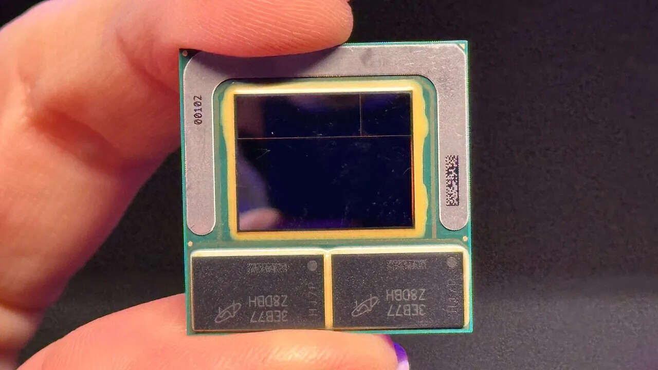
You can clearly see 3 tiles. Meteorlake has four. This is a legit Lunarlake sample. Lunarlake goes from tCPU, tGPU, tIO, tSoC in Meteorlake to (tCPU+GPU+IO) + tSoC. The third Lunarlake "tile" is a stiffner for structural integrity purposes and is a dummy die.
PrettyKitten800HyperThreading and SMT will both be phased out eventually. It's a workaround from 20 years ago and its simply not as effective as having more, smaller cores. Intel themselves have already proved this with their E cores. Every single non-x86 cpu doesn't use HT/SMT because it was never efficient enough to cut it in the handheld market, where efficiency gains mean performance gains. Designers have noticed this and begun applying the same logic to larger systems. Just look at the performance/watt of Apple M chips compared to their Intel and AMD counterparts. AMD is even using the same process node as Apple, but it still isn't competitive in this aspect. GPUs are also a great example. They have been multicore from the very start and no GPU design has ever incorporated HT/SMT.
They are giving up HT because while die size impact is small, it increases difficulty of validation. If removing HT allows the teams to execute better and get delayed less, the net impact is positive. Long term gain. Also HT has potential security issues. The modern many core trend reduces the impact of HT as well.
efikkanOr there is the very possible scenario where this new generation is so significantly more efficient so it doesn't need so much L3. L3 works very differently from L2, and is a spillover cache for all the cores.
No, in Lunarlake the E cores are no longer sharing the L3 like on predecessors. So it's 12MB L3 all for the P cores, and for the E cores it ends at L2. 2.5MB L2 + 3MB L3 for the P.

Also the E cores don't act like in predecessors either. They are more of a hybrid between Alder/Raptor's E cores and Meteorlake's LP E cores. It will serve the function LP E cores did and take over when the demand is low.
Posted on Reply
#14
pressing on
DavidC1The third Lunarlake "tile" is a stiffner for structural integrity purposes and is a dummy die.
A dummy die? Really? The interposer (base die) would provide any structural integrity needed I would have thought.
Posted on Reply
#15
DavidC1
pressing onA dummy die? Really? The interposer (base die) would provide any structural integrity needed I would have thought.
Yes.

And by the way Client leader Michelle Johnston Holthaus was shown holding Lunarlake in her hands. It was exactly as shown. In fact, the fingers that are cropped in OP's post are her fingers.

www.tomshardware.com/pc-components/cpus/intel-announces-arrow-lake-and-lunar-lake-will-arrive-in-2024-with-3-times-more-gpu-and-ai-acceleration-performance

It's also consistent with the massive leak a while ago: videocardz.com/newz/intel-lunar-lake-mx-leak-44-cpu-cores-8-xe2-gpu-cores-tsmc-n3b-node-and-displayport-2-1-support

Unlike Meteorlake which turned out to be a bit disappointing, with Lunarlake they'll make sound decisions. Meteorlake has too many tiles, just like Sapphire Rapids, and they both suffer from issues. Emerald Rapids moved to two tiles which improved memory and cache performance significantly and also perf/watt. The 8MB system level cache looks like to be a dedicated cache to save power by reducing access to memory. The LPE cores in MTL is only of marginal benefit, and the E cores are going to take that role too instead of area-efficient performance current E cores are for. At lower frequencies the E cores will be more power efficient as well and that's all you need as rather than adding performance it's only for low demand workloads.

Performance-wise, Lunarlake is a 4 core CPU, rather than a 4+4 one. Since Hyperthreading is said to be disabled on Lion Cove, we're looking at 4C/4T. Core-wise it isn't anything special other than being an expansion just like every P core Intel chip since Haswell and probably at least 20% faster per clock. At least the whole chip looks good. The big gain will be on the battery life side.

If you are looking for the highest laptop performance, this isn't for you. If you are looking for x86 platform that gets close(even match) to Apple Mx series in battery life in a small and light form factor, then you are looking in the right direction. Performance will be handled by another chip, code-named Arrowlake. Arrowlake unfortunately continues the 4-tile setup in Meteorlake, by swapping out the tCPU and tGPU. At least it should be a straight up upgrade.
Posted on Reply
#16
Wirko
DavidC1They are giving up HT because while die size impact is small, it increases difficulty of validation. If removing HT allows the teams to execute better and get delayed less, the net impact is positive. Long term gain. Also HT has potential security issues. The modern many core trend reduces the impact of HT as well.
That seems logical in a hybrid processor for the desktop or laptop. For interactive work, you need a couple of very fast cores, and a P core is very fast only as long as it runs a single thread.
Posted on Reply
#17
pressing on
DavidC1If you are looking for the highest laptop performance, this isn't for you. If you are looking for x86 platform that gets close(even match) to Apple Mx series in battery life in a small and light form factor, then you are looking in the right direction. Performance will be handled by another chip, code-named Arrowlake. Arrowlake unfortunately continues the 4-tile setup in Meteorlake, by swapping out the tCPU and tGPU. At least it should be a straight up upgrade.
Arrow Lake is Intel's desktop chip, probably called Series 2 replacing the former generation series of CPUs that ended with 14th gen. A new motherboard will be required so there is no upgrade path from the current Intel 600 and 700 series boards. Arrow Lake will have a similar architecture to Meteor Lake, but I don't quite get the too many tiles thing. The main improvement in the Meteor Lake laptops is the replacement of the former iGPU with a graphics tile that's a lot better than the previous iGPU, the spec of the graphics tile varies according to the CPU.

The six Meteor Lake U series CPUs are currently based on the same architecture as the H series. All U series have 2P + 8E + 2LPE, with Hyper Threading so 14 threads. All have 12Mb L3. The P cores vary between 4.4 and 4.9 GHz, the E cores between 3.6 and 3.8 GHz. It's possible that the CPU referred to in this leak might be a Lunar Lake version of one of these. The 12Mb L3 fits and if the firmware was gimped to only report the E cores that could also fit. The TDP of Meteor Lake U processors varies between 15W and 28W, in part because they have a very basic iGPU. There have been rumours of 9W devices. There have also been rumours of Meteor Lake CPUs with on-package LPDDR5X. So it might be a Meteor Lake device, or it might be a Lunar Lake device but whichever it is, it seems more likely to be a U rather than an H. The claim of an integrated graphics unit rather than a separate tile could make sense if the graphics capability is going to remain at the current level. It would mean Intel splitting the H and U series Lunar Lakes into two different architectures.
Posted on Reply
#18
DavidC1
pressing onArrow Lake is Intel's desktop chip, probably called Series 2 replacing the former generation series of CPUs that ended with 14th gen. A new motherboard will be required so there is no upgrade path from the current Intel 600 and 700 series boards. Arrow Lake will have a similar architecture to Meteor Lake, but I don't quite get the too many tiles thing. The main improvement in the Meteor Lake laptops is the replacement of the former iGPU with a graphics tile that's a lot better than the previous iGPU, the spec of the graphics tile varies according to the CPU. With the 155H for example for some users it might avoid the need to pay out for NVIDIA laptop chipsets.

The six Meteor Lake U series CPUs are currently based on the same architecture as the H series. All U series have 2P + 8E + 2LPE, with Hyper Threading so 14 threads. All have 12Mb L3. The P cores vary between 4.4 and 4.9 GHz, the E cores between 3.6 and 3.8 GHz. It's possible that the CPU referred to in this leak might be a Lunar Lake version of one of these. The 12Mb L3 fits and if the firmware was gimped to only report the E cores that could also fit. The TDP of Meteor Lake U processors varies between 15W and 28W, in part because they have a very basic iGPU. There have been rumours of 9W devices. There have also been rumours of Meteor Lake CPUs with on-package LPDDR5X. So it might be a Meteor Lake device, or it might be a Lunar Lake device but whichever it is, it seems more likely to be a U rather than an H. The claim of an integrated graphics unit rather than a separate tile could make sense if the graphics capability is going to remain at the current level.
Lunarlake is going to replace Meteorlake at the lower power envelopes, up to 30W, but going down to low as 8W for fanless. Then about similar time, Arrowlake comes for desktops, and replacing Meteorlake at the higher power laptop range. Also, they'll release a cheaper chip for low power laptops, but using same CPU architecture as Meteorlake but on Intel 3 instead.

Meteorlake P core is slower than Raptorlake at the same clock, likely due to Tiles. And AMD is still beating them with practically a last year's core in both absolute performance, performance at the same power level and battery life, that means it's bloated.

Also, stop and use your critical thinking skills man. That picture in the first post is Lunarlake. I gave you all the reasons why it is. Lunarlake is going to slap Meteorlake silly for what it matters for these laptops - battery life, thermals, and form factor.
Posted on Reply
#19
Random_User
Vayra86Hey look! Another Intel quad core :p
BTW judging by the picture it also looks like being "glued". Choose only the reputable "Snake oil" supplier.
Posted on Reply
#20
pressing on
Random_UserBTW judging by the picture it also looks like being "glued". Choose only the reputable "Snake oil" supplier.
Scanning the QR code on the CPU shown in the picture leads to a company called PHIX Photonics Assembly that says it "...provides an assembly and packaging service for photonic integrated circuits (PICs). We support chip prototypes as well as high-volume manufacturing." Now interestingly there was a story in late August/early September 2023 centred on details about a prototype silicon photonics CPU that had been released by Intel. This included a picture of this prototype (source: HotHardware)


The similarity between this image and the claimed Lunar Lake CPU is obvious. PHIX must be all out of glue. I am not saying that Lunar Lake is a silicon photonics CPU - it is more likely that Intel uses PHIX to assemble and package prototype processors of different kinds. But it is clearly a prototype, and how closely it resembles a production LL chip in terms of appearance or tile structure is anybody's guess.
Posted on Reply
Add your own comment
May 1st, 2024 22:08 EDT change timezone

New Forum Posts

Popular Reviews

Controversial News Posts