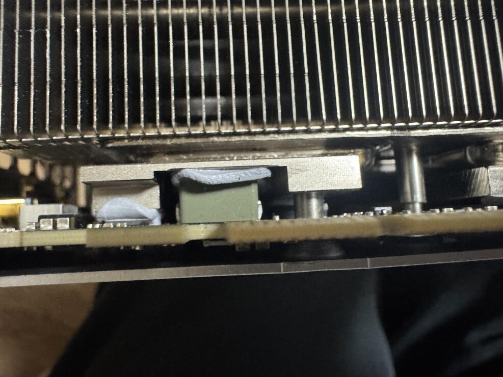
News Posts matching #South Korea

Return to Keyword Browsing

Report Suggests Naver Siding with Samsung in $752 Million "Mach-1" AI Chip Deal

Samsung debuted its Mach-1 generation of AI processors during a recent shareholder meeting—the South Korean megacorp anticipates an early 2025 launch window. Their application-specific integrated circuit (ASIC) design is expected to "excel in edge computing applications," with a focus on low power and efficiency-oriented operating environments. Naver Corporation was a key NVIDIA high-end AI customer in South Korea (and Japan), but the leading search platform firm and creator of HyperCLOVA X LLM (reportedly) deliberated on an adoption alternative hardware last October. The Korea Economic Daily believes that Naver's relationship with Samsung is set to grow, courtesy of a proposed $752 million investment: "the world's top memory chipmaker, will supply its next-generation Mach-1 artificial intelligence chips to Naver Corp. by the end of this year."

Reports from last December indicated that the two companies were deep into the process of co-designing power-efficient AI accelerators—Naver's main goal is to finalize a product that will offer eight times more energy efficiency than NVIDIA's H100 AI accelerator. Naver's alleged bulk order—of roughly 150,000 to 200,000 Samsung Mach-1 AI chips—appears to be a stopgap. Industry insiders reckon that Samsung's first-gen AI accelerator is much cheaper when compared to NVIDIA H100 GPU price points—a per-unit figure of $3756 is mentioned in the KED Global article. Samsung is speculated to be shopping its fledgling AI tech to Microsoft and Meta.

EMTEK Launches GeForce RTX 4070 SUPER MIRACLE X3 White 12 GB Graphics Card

EMTEK products rarely pop up on TPU's news section, but the GPU database contains a smattering of the South Korean manufacturer's Ampere-based GeForce RTX graphics card. VideoCardz has discovered an updated MIRACLE X3 White model—EMTEK's latest release is a GeForce RTX 4070 SUPER 12 GB card. The triple-fan model seems to stick with NVIDIA's reference specifications—VideoCardz also noticed a physical similarity: "under the cooler shroud, the card boasts a non-standard U-shaped PCB, reminiscent of Team Green's Founders Edition. However, it remains uncertain whether EMTEK utilizes the same PCB as NVIDIA." The asking price—of ₩919,990—converts to around $680, when factoring in regional taxes. EMTEK's MIRACLE X3 cooling solution seems to be fairly robust—featuring four 6 mm heat pipes—so an adherence to stock clocks is a slight surprise. The company's GAMING PRO line includes a couple of factory overclocked options.

Samsung Prepares Mach-1 Chip to Rival NVIDIA in AI Inference

During its 55th annual shareholders' meeting, Samsung Electronics announced its entry into the AI processor market with the upcoming launch of its Mach-1 AI accelerator chips in early 2025. The South Korean tech giant revealed its plans to compete with established players like NVIDIA in the rapidly growing AI hardware sector. The Mach-1 generation of chips is an application-specific integrated circuit (ASIC) design equipped with LPDDR memory that is envisioned to excel in edge computing applications. While Samsung does not aim to directly rival NVIDIA's ultra-high-end AI solutions like the H100, B100, or B200, the company's strategy focuses on carving out a niche in the market by offering unique features and performance enhancements at the edge, where low power and efficient computing is what matters the most.

According to SeDaily, the Mach-1 chips boast a groundbreaking feature that significantly reduces memory bandwidth requirements for inference to approximately 0.125x compared to existing designs, which is an 87.5% reduction. This innovation could give Samsung a competitive edge in terms of efficiency and cost-effectiveness. As the demand for AI-powered devices and services continues to soar, Samsung's foray into the AI chip market is expected to intensify competition and drive innovation in the industry. While NVIDIA currently holds a dominant position, Samsung's cutting-edge technology and access to advanced semiconductor manufacturing nodes could make it a formidable contender. The Mach-1 has been field-verified on an FPGA, while the final design is currently going through a physical design for SoC, which includes placement, routing, and other layout optimizations.

New Xbox Development Kit Certified by South Korean Agency

Yesterday, South Korea's National Radio Research Agency certified a brand new and very mysterious Xbox Development Kit—naturally, the "Xbox News for Koreans" social media account took credit for this intriguing discovery: "this means that you can use the device in Korea. It is likely to be distributed to game developers in Korea soon." The model's serial code—2089—does not correspond to any of Microsoft's current Xbox Series (X|S) development kits. The tipster shared a short history lesson: "Xbox Series X|S dev kit consoles were certified by the National Radio Research Agency on June 10-11, 2020. The release of the Xbox Series X|S console in Korea was on November 10, 2020." By referencing the current generation's five-month gap—between registration and release of finalized retail units—it is speculated that something new could be arriving around August time.

Industry experts reckon that the leaked devkit is not linked to a rumored "All-Digital" White Xbox Series X Refresh—the latter likely contains unchanged basic hardware designs. Windows Central posited that an Xbox handheld is another possibility—leaked product roadmaps (of 2022 vintage) revealed that Microsoft was considering a move into portable gaming segments. A month ago, Xbox leadership discussed the platform's future—Sarah Bond stated: "there's some exciting stuff coming out in hardware that we're going to share this holiday, and we're also invested in the next generation roadmap...and what we're really focused on there, is delivering the largest technical leap you will have ever seen in a hardware generation." Many media outlets believed that an Xbox Series "Pro" model was teased during the special Official Xbox Videocast.

Samsung Expected to Unveil Enterprise "PBSSD" Subscription Service at GTC

Samsung Electronics is all set to discuss the future of AI, alongside Jensen Huang, at NVIDIA's upcoming GTC 2024 conference. South Korean insiders have leaked the company's intentions, only days before the event's March 18 kickoff time. Their recently unveiled 36 GB HBM3E 12H DRAM product is expected to be the main focus of official presentations—additionally, a new storage subscription service is marked down for a possible live introduction. An overall "Redefining AI Infrastructure" presentation could include—according to BusinessKorea—a planned launch of: "petabyte (PB)-level SSD solution, dubbed 'PBSSD,' along with a subscription service in the US market within the second quarter (of 2024) to address the era of ultra-high-capacity data."

A Samsung statement—likely sourced from leaked material—summarized this business model: "the subscription service will help reduce initial investment costs in storage infrastructure for our customers and cut down on maintenance expenses." Under agreed upon conditions, customers are not required to purchasing ultra-high-capacity SSD solutions outright: "enterprises using the service can flexibly utilize SSD storage without the need to build separate infrastructure, while simultaneously receiving various services from Samsung Electronics related to storage management, security, and upgrades." A special session—"The Value of Storage as a Service for AI/ML and Data Analysis"—is alleged to be on the company's GTC schedule.

Samsung Reportedly Acquiring New Equipment Due to Disappointing HBM Yields

Industry insiders reckon that Samsung Electronics is transitioning to molded underfill (MR-MUF) production techniques—rival memory manufacturer, SK Hynix, champions this chip making technology. A Reuters exclusive has cited claims made by five industry moles—they believe that Samsung is reacting to underwhelming HBM production yields. The publication proposes that: "one of the reasons Samsung has fallen behind (competing producers) is its decision to stick with chip making technology called non-conductive film (NCF) that causes some production issues, while Hynix switched to the mass reflow molded underfill (MR-MUF) method to address NCF's weakness." The report suggests that Samsung is in the process of ordering new MUF-related equipment.

One anonymous source stated: "Samsung had to do something to ramp up its HBM (production) yields... adopting MUF technique is a little bit of swallow-your-pride type thing for (them), because it ended up following the technique first used by SK Hynix." Reuters managed to extract a response from the giant South Korean multinational—a company spokesperson stated: "we are carrying out our HBM3E product business as planned." They indicated that NCF technology remains in place as an "optimal solution." Post-publication, another official response was issued: "rumors that Samsung will apply MR-MUF to its HBM production are not true." Insiders propose a long testing phase—Samsung is rumored to be sourcing MUF materials, but mass production is not expected to start this year. Three insiders allege that Samsung is planning to "use both NCF and MUF techniques" for a new-generation HBM chip.

NVIDIA's Selection of Micron HBM3E Supposedly Surprises Competing Memory Makers

SK Hynix believes that it leads the industry with the development and production of High Bandwidth Memory (HBM) solutions, but rival memory manufacturers are working hard on equivalent fifth generation packages. NVIDIA was expected to select SK Hynix as the main supplier of HBM3E parts for utilization on H200 "Hopper" AI GPUs, but a surprise announcement was issued by Micron's press team last month. The American firm revealed that HBM3E volume production had commenced: ""(our) 24 GB 8H HBM3E will be part of NVIDIA H200 Tensor Core GPUs, which will begin shipping in the second calendar quarter of 2024. This milestone positions Micron at the forefront of the industry, empowering artificial intelligence (AI) solutions with HBM3E's industry-leading performance and energy efficiency."

According to a Korea JoongAng Daily report, this boast has reportedly "shocked" the likes of SK Hynix and Samsung Electronics. They believe that Micron's: "announcement was a revolt from an underdog, as the US company barely held 10 percent of the global market last year." The article also points out some behind-the-scenes legal wrangling: "the cutthroat competition became more evident when the Seoul court sided with SK Hynix on Thursday (March 7) by granting a non-compete injunction to prevent its former researcher, who specialized in HBM, from working at Micron. He would be fined 10 million won for each day in violation." SK Hynix is likely pinning its next-gen AI GPU hopes on a 12-layer DRAM stacked HBM3E product—industry insiders posit that evaluation samples were submitted to NVIDIA last month. The outlook for these units is said to be very positive—mass production could start as early as this month.

JEDEC Agrees to Relax HBM4 Package Thickness

JEDEC is currently presiding over standards for 6th generation high bandwidth memory (AKA HBM4)—the 12 and 16-layer DRAM designs are expected to reach mass production status in 2026. According to a ZDNET South Korea report, involved manufacturers are deliberating over HBM4 package thicknesses—allegedly, decision makers have settled on 775 micrometers (μm). This is thicker than the previous generation's measurement of 720 micrometers (μm). Samsung Electronics, SK Hynix and Micron are exploring "hybrid bonding," a new packaging technology—where onboard chips and wafers are linked directly to each other. Hybrid bonding is expected to be quite expensive to implement, so memory makers are carefully considering whether HBM4 warrants its usage.

ZDNET believes that JEDEC's agreement—settling on 775 micrometers (μm) for 12-layer and 16-layer stacked HBM4—could have: "a significant impact on the future packaging investment trends of major memory manufacturers. These companies have been preparing a new packaging technology, hybrid bonding, keeping in mind the possibility that the package thickness of HBM4 will be limited to 720 micrometers. However, if the package thickness is adjusted to 775 micrometers, 16-layer DRAM stacking HBM4 can be sufficiently implemented using existing bonding technology." A revised schedule could delay the rollout of hybrid bonding—perhaps pushed back to coincide with a launch of seventh generation HBM. The report posits that Samsung Electronics, SK Hynix and Micron memory engineers are about to focus on the upgrading of existing bonding technologies.

Samsung Accelerates R&D of Glass Substrate Chip Packaging

The Samsung Group has formed a new cross-department alliance—according to South Korea's Sedaily—this joint operation will concentrate on the research and development of a "dream substrate." The company's Electronics, Electrical Engineering, and Display divisions are collaborating in order to accelerate commercialization of "glass substrate" chip packaging. Last September, Intel revealed its intention to become an industry leader in "glass substrate production for next-generation advanced packaging." Team Blue's shiny new Arizona fabrication site will be taking on this challenge, following ten years of internal R&D work. Industry watchdogs reckon that mass production—in North America—is not expected to kick off anytime soon. Sensible guesstimates suggest a start date somewhere in 2030.

The Sedaily article states that Samsung's triple department alliance will target "commercialization faster than Intel." Company representatives—in attendance at CES 2024—set a 2026 window as their commencement goal for advanced glass substrate chip package mass production. An unnamed South Korean industry watcher has welcomed a new entrant on the field: "as each company possesses the world's best technology, synergies will be maximized in glass substrate research, which is a promising field...it is also important to watch how the glass substrate ecosystem of Samsung's joint venture will be established." Glass substrate packaging is ideal for "large-area and high-performance chip combinations" due to inherent heat-resistant properties and material strength. So far, the semiconductor industry has struggled with its development—hence the continued reliance on plastic boards and organic materials.

NVIDIA Reportedly Sampling SK Hynix 12-layer HBM3E

South Korean tech insiders believe that SK Hynix has sent "12-layer DRAM stacked HBM3E (5th generation HBM)" prototype samples to NVIDIA—according a ZDNET.co.kr article, initial examples were shipped out last month. Reports from mid-2023 suggested that Team Green had sampled 8-layer HBM3E (4th gen) units around summer time—with SK Hynix receiving approval notices soon after. Another South Korean media outlet, DealSite, reckons that NVIDIA's memory qualification process has exposed HBM yield problems across a number of manufacturers. SK Hynix, Samsung and Micron are competing fiercely on the HBM3E front—with hopes of getting their respective products attached to NVIDIA's H200 AI GPU. DigiTimes Asia proposed that SK Hynix is ready to "commence mass production of fifth-generation HBM3E" at some point this month.

SK Hynix is believed to be leading the pack—insiders believe that yield rates are good enough to pass early NVIDIA certification, and advanced 12-layer samples are expected to be approved in the near future. ZDNET reckons that SK Hynix's forward momentum has placed it an advantageous position: "(They) supplied 8-layer HBM3E samples in the second half of last year and passed recent testing. Although the official schedule has not been revealed, mass production is expected to begin as early as this month. Furthermore, SK Hynix supplied 12-layer HBM3E samples to NVIDIA last month. This sample is an extremely early version and is mainly used to establish standards and characteristics of new products. SK Hynix calls it UTV (Universal Test Vehicle)... Since Hynix has already completed the performance verification of the 8-layer HBM3E, it is expected that the 12-layer HBM3E test will not take much time." SK Hynix's Vice President recently revealed that his company's 2024 HBM production volumes for were already sold out, and leadership is already preparing innovations for 2025 and beyond.

Samsung Foundry Renames 3 nm Process to 2 nm Amid Competition with Intel

In a move that could intensify competition with Intel in the cutting-edge chip manufacturing space, Samsung Foundry has reportedly decided to rebrand its second-generation 3 nm-class fabrication technology, previously known as SF3, to a 2 nm-class manufacturing process called SF2. According to reports from ZDNet, the renaming of Samsung's SF3 to SF2 is likely an attempt by the South Korean tech giant to simplify its process nomenclature and better compete against Intel Foundry, at least visually. Intel is set to roll out its Intel 20A production node, a 2 nm-class technology, later this year. The reports suggest that Samsung has already notified its customers about the changes in its roadmap and the renaming of SF3 to SF2. Significantly, the company has reportedly gone as far as re-signing contracts with customers initially intended to use the SF3 production node.

"We were informed by Samsung Electronics that the 2nd generation 3 nm [name] is being changed to 2 nm," an unnamed source noted to ZDNet. "We had contracted Samsung Foundry for the 2nd generation 3 nm production last year, but we recently revised the contract to change the name to 2 nm." Despite the name change, Samsung's SF3, now called SF2, has not undergone any actual process technology alterations. This suggests that the renaming is primarily a marketing move, as using a different process technology would require customers to rework their chip designs entirely. Samsung intends to start manufacturing chips based on the newly named SF2 process in the second half of 2024. The SF2 technology, which employs gate-all-around (GAA) transistors that Samsung brands as Multi-Bridge-Channel Field Effect Transistors (MBCFET), does not feature a backside power delivery network (BSPDN), a significant advantage of Intel's 20A process. Samsung Foundry has not officially confirmed the renaming.

Samsung Reportedly Working on Backside Power Supply Tech with 2 Nanometer Process

Samsung and ARM announced a collaborative project last week—the partners are aiming to deliver an "optimized next generation Arm Cortex -X CPU" developed on the latest Gate-All-Around (GAA) process technology. Semiconductor industry watchdogs believe that Samsung Foundry's 3 nm GAA process did not meet sales expectations—reports suggest that many clients decided to pursue advanced three nanometer service options chez TSMC. The South Korean multinational manufacturing conglomerate is setting its sights forward—with an in-progress SF2 GAAFET process in the pipeline—industry insiders reckon that Samsung leadership is hoping to score a major victory within this next-gen market segment.

Lately, important industry figures have been hyping up Backside Power Supply Delivery Network (BSPDN) technology—recent Intel Foundry Services (IFS) press material lays claim to several technological innovations. A prime example being an ambitious five-nodes-in-four-years (5N4Y) process roadmap that: "remains on track and will deliver the industry's first backside power solution." A Chosun Business report proposes that Samsung is working on Backside Power Supply designs—a possible "game changer" when combined with in-house 2 nm SF2 GAAFET. Early experiments, allegedly, involving two unidentified ARM cores have exceeded expectations—according to Chosun's sources, engineers were able to: "reduce the chip area by 10% and 19%, respectively, and succeeded in improving chip performance and frequency efficiency to a single-digit level." Samsung Foundry could be adjusting its mass production timetables, based on freshly reported technological breakthroughs—SF2 GAAFET + BSPDN designs could arrive before the original targeted year of 2027. Prior to the latest developments, Samsung's BSPDN tech was linked to a futuristic 1.7 nm line.

Samsung Foundry Reportedly Producing 2 nm Prototypes for Qualcomm

Smartphone chipset industry watchdogs believe that the Samsung 3 nm GAA process did not meet customer expectations, due to alleged yield issues. TSMC is seemingly victorious in this segment, as reports suggest that a next-generation 3 nm node production goal of "100,000 monthly wafers by the end of 2024" has been set. Three days ago, Samsung Foundry revealed that it is working on a very advanced SF2 GAAFET process—press outlets in South Korea propose that the manufacturing giant is hoping to outmuscle its main rival in a future 2 nm node category. Tuesday's press introduction stated that a development partnership is set: "to deliver optimized next generation ARM Cortex -X CPU developed on Samsung Foundry's latest Gate-All-Around (GAA) process technology."

A Sedaily article posits that the company's cutting-edge manufacturing tech has already attracted interest from notable parties: "Samsung Electronics is taking advantage of these advantages to win orders for the 2 nm project. Samsung Electronics took its first step by winning an order to produce a 2 nm AI accelerator from Preferred Networks (PFN), Japan's largest AI company. Qualcomm, the world's largest system semiconductor design company, has entered into discussions with Samsung Electronics' System LSI Division, which designs high-performance chips, to produce 2 nm prototypes." December 2023 news reports suggested that Samsung leadership was considering a 2 nm wafer price discount—in order to stay competitive with competing foundry services. It is possible that Qualcomm is evaluating the 2 nm SF2 GAAFET process for a distant Snapdragon 8 "Gen 5" chipset, while Samsung LSI could be working on a 2 nm "Exynos 2600" SoC design.

SK Hynix VP Reveals HBM Production Volumes for 2024 are Sold Out

SK Hynix Vice President Kitae Kim presides over the company's HBM Sales & Marketing (S&M) department—an official leadership blog profile reveals that the executive played a key role in making the South Korean supplier's high bandwidth memory (HBM) product line "a superstar of the semiconductor memory industry in 2023." Growing demand for powerful AI processors has placed SK Hynix in a more comfortable position, following recessive spells—including a major sales downturn in 2022. NVIDIA is the market leader in AI processing chips, and many of its flagship enterprise designs are fitted with cutting-edge SK Hynix memory modules. Kim noted that his firm has many notable international clients: "HBM is a revolutionary product which has challenged the notion that semiconductor memory is only one part of an overall system...in particular, SK Hynix's HBM has outstanding competitiveness. Our advanced technology is highly sought after by global tech companies."

The VP outlined how artificial intelligence industries are fuelling innovations: "With the diversification and advancement of generative AI services, demand for HBM, an AI memory solution, has also exploded. HBM, with its high-performance and high-capacity characteristics, is a monumental product that shakes the conventional wisdom that memory semiconductors are only a part of the overall system. In particular, SK Hynix HBM's competitiveness is outstanding." Business is booming, so much so that nothing can be added to this year's HBM order books: "Proactively securing customer purchase volumes and negotiating more favorable conditions for our high-quality products are the basics of semiconductor sales operations. With excellent products in hand, it's a matter of speed. Our planned production volume of HBM this year has already sold out. Although 2024 has just begun, we've already started preparing for 2025 to stay ahead of the market."

Insiders Predict Slimmer Profiles on 2024 iPad Pro OLED Models

Mid-January reportage indicated that LG and Samsung plants in South Korea had commenced construction of next-gen Apple iPad OLED parts—while expert analysis has predicted a second quarter launch of 11 and 13-inch "Pro" tablet models. Omdia—an independent analyst and consultancy firm—has compiled its Apple field research into a forecasted roadmap of various portable products. Company analysts believe that: "LG Display (LGD) and Samsung Display (SDC) are preparing to mass-produce RGB tandem stack and Hybrid OLEDs from their half-Gen 6 fabs. Apple also plans to launch the MacBook Pro with OLED displays in 2026. BOE, LGD, and SDC are preparing their fab investments to produce RGB tandem stack and hybrid OLEDs at half-Gen 8.7 fabs."

9to5Mac's insider network detected whispers of possible Apple tablet physical profile adjustments—suggesting that a larger next-gen iPad Air is in the pipeline, alongside a thinner iPad Pro design update: "(we) first reported last year that Apple has been working on two new versions of the iPad Air, codenamed J507 and J537. While one of these models will look pretty much like the current iPad Air, the other will have a larger display. If true, this will be the first time Apple will offer the iPad Air in two different sizes. And according to our sources, this larger iPad Air will have essentially the same dimensions as the current 12.9-inch iPad Pro, suggesting that the screen size will also be almost identical. The smaller iPad Air is unlikely to have any significant design changes."

Kioxia Reportedly Presents Japanese Chipmaking Deal to SK Hynix

Japan's Jiji news agency has cottoned onto a major computer memory industry rumble—a Friday Reuters report suggests that Kioxia has offered an olive branch to SK Hynix, perhaps in a renewed push to get its proposed (and once rejected) merger with Western Digital over the finishing line. The South Korean memory manufacturing juggernaut took great issue with the suggested formation of a mighty Japanese-American 3D NAND memory chip conglomerate—SK Hynix's opposition reportedly placed great pressure on Western Digital (WD), and discussions with Kioxia ended last October.

Kioxia is seemingly eager to resume talks with WD, but requires a thumbs up from SK Hynix—according to Jiji's insider source(s), the Tokyo-headquartered manufacturer is prepared to offer its South Korean rival a nice non-volatile memory production deal. Kioxia's best Japanese 3D NAND fabrication facilities could play host to SK Hynix designs, although it is too early to tell whether this bid has been accepted. The Yokkaichi and Kitakami plants are set to receive a 150 billion yen Government subsidy—Kioxia and WD's joint venture is expected to move into cutting-edge semiconductor production. The Japanese government is hoping to secure its native operations in times of industry flux.

TSMC & SK Hynix Reportedly Form Strategic AI Alliance, Jointly Developing HBM4

Last week SK Hynix revealed ambitious plans for its next wave of High Bandwidth Memory (HBM) products—their SEMICON Korea 2024 presentation included an announcement about cutting-edge HBM3E entering mass production within the first quarter of this year. True next-gen HBM development has already kicked off—TPU's previous report outlines an HBM4 sampling phase in 2025, followed by full production in 2026. South Korea's Pulse News believes that TSMC has been roped into a joint venture (with SK Hynix). An alleged "One Team" strategic alliance has been formed according to reports emerging from Asia—this joint effort could focus on the development of HBM4 solutions for AI fields.

Reports from last November pointed to a possible SK Hynix and NVIDIA HBM4 partnership, with TSMC involved as the designated fabricator. We are not sure if the emerging "One Team" progressive partnership will have any impact on previously agreed upon deals, but South Korean news outlets reckon that the TSMC + SK Hynix alliance will attempt to outdo Samsung's development of "new-generation AI semiconductor packaging." Team Green's upcoming roster of—"Hopper" H200 and "Blackwell" B100—AI GPUs are linked to a massive pre-paid shipment of SK Hynix HMB3E parts. HBM4 products could be fitted on a second iteration of NVIDIA's Blackwell GPU, and the mysterious "Vera Rubin" family. Notorious silicon industry tipster, kopite7kimi, believes that "R100 and GR200" GPUs are next up in Team Green's AI-cruncher queue.

Korea Quantum Computing Signs IBM watsonx Deal

IBM has announced (on January 29) that Korea Quantum Computing (KQC) has engaged IBM to offer IBM's most advanced AI software and infrastructure, as well as quantum computing services. KQC's ecosystem of users will have access to IBM's full stack solution for AI, including watsonx, an AI and data platform to train, tune and deploy advanced AI models and software for enterprises. KQC is also expanding its quantum computing collaboration with IBM. Having operated as an IBM Quantum Innovation Center since 2022, KQC will continue to offer access to IBM's global fleet of utility-scale quantum systems over the cloud. Additionally, IBM and KQC plan to deploy an IBM Quantum System Two on-site at KQC in Busan, South Korea by 2028.

"We are excited to work with KQC to deploy AI and quantum systems to drive innovation across Korean industries. With this engagement, KQC clients will have the ability to train, fine-tune, and deploy advanced AI models, using IBM watsonx and advanced AI infrastructure. Additionally, by having the opportunity to access IBM quantum systems over the cloud, today—and a next-generation quantum system in the coming years—KQC members will be able to combine the power of AI and quantum to develop new applications to address their industries' toughest problems," said Darío Gil, IBM Senior Vice President and Director of Research. This collaboration includes an investment in infrastructure to support the development and deployment of generative AI. Plans for the AI-optimized infrastructure includes advanced GPUs and IBM's Artificial Intelligence Unit (AIU), managed with Red Hat OpenShift to provide a cloud-native environment. Together, the GPU system and AIU combination is being engineered to offer members state-of-the-art hardware to power AI research and business opportunities.

HBM Industry Revenue Could Double by 2025 - Growth Driven by Next-gen AI GPUs Cited

Samsung, SK hynix, and Micron are considered to be the top manufacturing sources of High Bandwidth Memory (HBM)—the HBM3 and HBM3E standards are becoming increasingly in demand, due to a widespread deployment of GPUs and accelerators by generative AI companies. Taiwan's Commercial Times proposes that there is an ongoing shortage of HBM components—but this presents a growth opportunity for smaller manufacturers in the region. Naturally, the big name producers are expected to dive in head first with the development of next generation models. The aforementioned financial news article cites research conducted by the Gartner group—they predict that the HBM market will hit an all-time high of $4.976 billion (USD) by 2025.

This estimate is almost double that of projected revenues (just over $2 billion) generated by the HBM market in 2023—the explosive growth of generative AI applications has "boosted" demand for the most performant memory standards. The Commercial Times report states that SK Hynix is the current HBM3E leader, with Micron and Samsung trailing behind—industry experts believe that stragglers will need to "expand HBM production capacity" in order to stay competitive. SK Hynix has shacked up with NVIDIA—the GH200 Grace Hopper platform was unveiled last summer; outfitted with the South Korean firm's HBM3e parts. In a similar timeframe, Samsung was named as AMD's preferred supplier of HBM3 packages—as featured within the recently launched Instinct MI300X accelerator. NVIDIA's HBM3E deal with SK Hynix is believed to extend to the internal makeup of Blackwell GB100 data-center GPUs. The HBM4 memory standard is expected to be the next major battleground for the industry's hardest hitters.

Kioxia and Western Digital Could Announce Merger This Month

According to Kyodo News, Japanese chip manufacturer Kioxia and its U.S. counterpart Western Digital are reportedly on the verge of finalizing a merger agreement, aiming to create the world's largest producer of memory chips. The merger plan involves establishing a holding company to consolidate their operations for producing NAND flash memory chips, with the announcement reportedly coming this month. The merged entity is expected to be listed on the Nasdaq stock exchange in the United States. As the global semiconductor market contends with competitive pressures and fluctuating demand, the merger is seen as a strategic move to enhance the combined market position of both companies.

Western Digital shareholders are anticipated to hold a majority stake in the new entity, with Kioxia's shareholders, including Toshiba Corporation, owning the remaining stake. The move is poised to give the newly formed company a combined market share of 35.4 percent in NAND memory chips as of March, surpassing South Korea's Samsung, the current leader, with 34.3 percent. However, the merger's ultimate approval hinges on regulators' decisions, including those in China, as semiconductors have become increasingly integral to global economic security. Major Japanese banks, including MUFG Bank and the state-backed Development Bank of Japan, are contemplating loans of up to approximately 1.9 trillion yen (about $12.7 billion) to facilitate the merger.

FSP's 2023 PSU Lineup Updated with ATX 3.0 "12V-2×6" Standard

FSP has declared that it intends to update its entire 2023 PSU product lineup to include the latest "12V-2x6" power connector (part of the ATX 3.0 standard)—harukaze5719 posted about this development earlier today, citing a Quasarzone article. We heard mid-summer about PCI-SIG plowing ahead on an all-new ATX 3.0 connector to replace the 16-pin (12+4) 12VHPWR plug. They hope to introduce some key improvements with their new design, mainly in the areas of ease-of-use and safety.

TPU staffers had hands-on time with FSP's 2023 PSU product line at their Computex 2023 booth, showcased units were equipped with 16-pin 12VHPWR (at the time). Quasarzone's report (covering a recent press conference) has the following FSP power supply families listed with updates to the new "12V-2x6" standard: Hydro G PRO 1200 W ATX 3.0, Hydro PTM X PRO ATX 3.0 and Dagger PRO ATX 3.0.

Samsung Teases Upcoming Launch of 990 Pro SSD 4 TB Model

Samsung Semiconductor introduced its 990 PRO Flagship PCIe Gen 4 SSD range a year ago, with 1 TB and 2 TB models available day one on launch. The South Korean company also teased a 4 TB variant for release in 2023—recent activity on social media indicates that the higher capacity model will be coming soon (but no firm date was touted): "You wanted it so badly, we had no choice but to deliver. The 4 TB 990 PRO by Samsung SSD is coming. Same blazing-fast storage with double the max capacity for gaming, video, 3D editing, and more. Stay tuned for more details."

According to Samsung's specification sheet, the 990 Pro 4 TB is due to arrive in two forms—a plain drive (MZ-V9P4T0BW) with a simple/thin graphene heat spreader and a fancier version sporting an aluminium heatsink (MZ-V9P4T0CW). The latest marketing blurb continues to place emphasis on the 990 Pro M.2 2280 drives being ideal candidates for upgrading the PlayStation 5's (PCIe 4.0) internal storage—we will have to wait closer to launch time for the 4 TB variant's MSRP, although its eventual pricing is most likely going to target enthusiast PC users. The 2 TB model (w/ heatsink) is currently available for $149.99 (down from the original launch value of $309.99) at the time of writing.

Samsung & MediaTek Announce Industry-first 3Tx Antenna Transmission

Samsung Electronics and MediaTek completed the successful testing of 5G Standalone Uplink (UL) 2CC Carrier Aggregation (CA) with C-Band UL MIMO to reach top uplink speeds, marking a groundbreaking achievement in wireless mobile capabilities. This approach used three transmit (3Tx) antennas to improve upload experiences, ushering in an era of enhanced connectivity for consumers worldwide.

The demands on uplink performance are increasing with the rise of live streaming, multi-player gaming and video conferences. Upload speeds determine how fast your device can send data to gaming servers or transmit high-resolution videos to the cloud. As more consumers seek to document and share their experiences with the world in real-time, enhanced uplink experiences provide an opportunity to use the network to improve how they map out their route home, check player stats online and upload videos and selfies to share with friends and followers.

Samsung Electronics Unveils Foundry Vision in the AI Era

Samsung Electronics, a world leader in advanced semiconductor technology, today announced its latest foundry technology innovations and business strategy at the 7th annual Samsung Foundry Forum (SFF) 2023. Under the theme "Innovation Beyond Boundaries," this year's forum delved into Samsung Foundry's mission to address customer needs in the artificial intelligence (AI) era through advanced semiconductor technology.

Over 700 guests, from customers and partners of Samsung Foundry, attended this year's event, of which 38 companies hosted their own booths to share the latest technology trends in the foundry industry.

Quake II Remastered Outed by South Korean Ratings Board

Gematsu - a Japanese news site - has discovered that the Game Rating and Administration Committee of Korea uploaded its rating of an announced remake of Quake II (1997) on May 31—apparently "not suitable" for youths. This could repeat a pattern from 2021, where the same committee registered the original Quake's remastered version prior to an official unveiling at that year's livestreamed QuakeCon event.

QuakeCon 2023 is heading back to its roots—with a return to an in-person format "at the Gaylord Texan Resort & Convention Center in Grapevine, Texas from Thursday, August 10 through Sunday, August 13." It is quite possible that Quake II Remastered will get an unveiling at the late summer convention. It will be interesting to see how the upcoming remaster will sit beside the existing RTX version—the South Korean rating info mentions new online multiplayer options, 4K resolution plus widescreen support, as well as support for community modification.
Return to Keyword Browsing
Apr 25th, 2024 18:31 EDT change timezone

New Forum Posts

Popular Reviews

Controversial News Posts