Report an Error


ATI M72
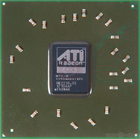
M72

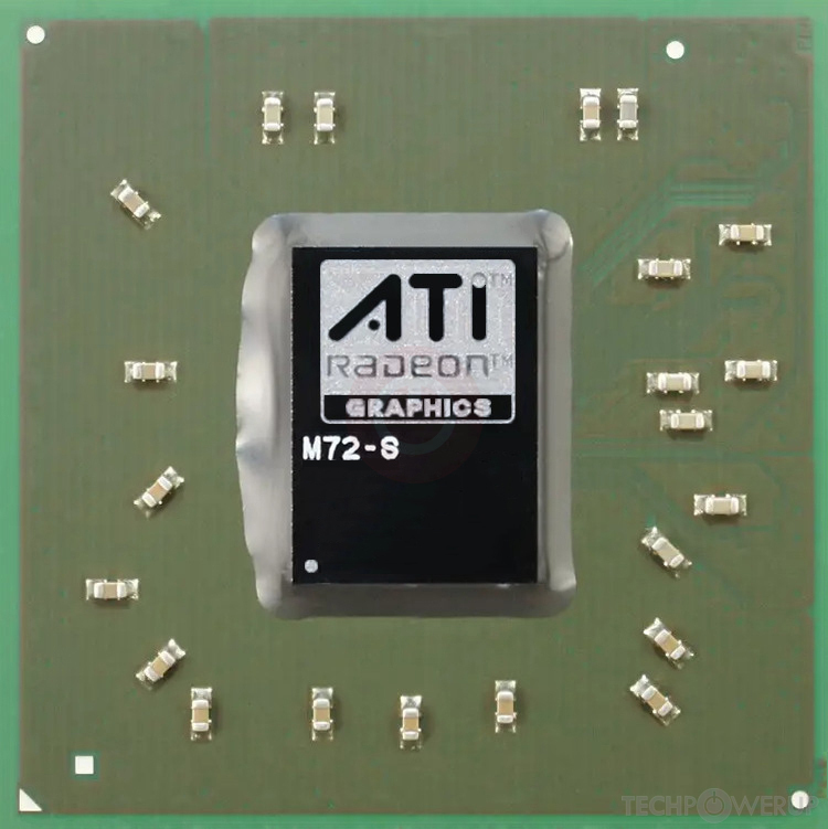
M72-S

M72-M

Block Diagram
ATI's M72 GPU uses the TeraScale architecture and is made using a 65 nm production process at TSMC. With a die size of 85 mm² and a transistor count of 180 million it is a very small chip. M72 supports DirectX 10.0 (Feature Level 10_0). For GPU compute applications, OpenCL version N/A can be used. It features 40 shading units, 4 texture mapping units and 4 ROPs.
Further reading:
R600 Series Instruction Set Architecture 
Graphics Processor
- Released
- May 14th, 2007
- GPU Name
- M72
- Desktop Variant
- RV610
- Codename
- Laka
- Architecture
- TeraScale
- Foundry
- TSMC
- Process Size
- 65 nm
- Transistors
- 180 million
- Density
- 2.1M / mm²
- Die Size
- 85 mm²
- Package
- FCBGA-632/880
Graphics Features
- DirectX
- 10.0 (10_0)
- OpenGL
- 3.3
- OpenCL
- N/A
- Vulkan
- N/A
- Shader Model
- 4.0
- WDDM
- 1.1
- Compute
- GFX3
- DCE
- 2.0
- UVD
- 1.0
Render Config
- Shading Units
- 40
- TMUs
- 4
- ROPs
- 4
- Compute Units
- 2
- Vertex Cache
- 32 KB
- Texture Cache
- 32 KB
- Tex L1 Cache
- 32 KB per 4 SPs
- L2 Cache
- 32 KB
All TeraScale GPUs
- ATI M72
- ATI M74
- ATI M76
- ATI M82
- ATI M84
- ATI M86
- ATI M88
- ATI M92
- AMD M93
- ATI M93
- ATI M96
- ATI M97
- ATI M98
- ATI R600
- ATI R680
- ATI R700
- ATI RS780
- ATI RS880
- ATI RV610
- ATI RV620
- ATI RV630
- ATI RV635
- ATI RV670
- AMD RV670
- ATI RV710
- AMD RV711
- ATI RV711
- ATI RV730
- ATI RV740
- ATI RV770
- AMD RV770
- ATI RV790
- ATI RX881
- ATI Theater 650 PRO
- ATI Xenos Corona
- ATI Xenos Falcon
- ATI Xenos Jasper
- ATI Xenos Vejle
- ATI Xenos Xenon
ATI GPU Architecture History
Graphics cards using the ATI M72 GPU
| Name | Chip | Memory | Shaders | TMUs | ROPs | GPU Clock | Memory Clock |
|---|---|---|---|---|---|---|---|
| M72-S | 256 MB | 40 | 4 | 4 | 450 MHz | 400 MHz |

M72 GPU Notes
| Desktop Variant: RV610 Codename: Laka Graphics/Compute: GFX3 Display Core Engine: 2.0 Unified Video Decoder: 1.0 |
May 20th, 2024 18:29 EDT
change timezone
Latest GPU Drivers
New Forum Posts
- My anti budget PC (42)
- Inland 512GB SATA SSD; reliable? (6)
- For general use - moving files around and playing games, would you have an Optane boot drive or PCie gen 5? (55)
- GTA VI Now Slated For Launch in Fall of Next Year (1)
- TPU's Nostalgic Hardware Club (18514)
- What's your latest tech purchase? (20595)
- Fractal define R4 vs R5 build quality. (18)
- Samsung 870 EVO - Beware, certain batches prone to failure! (1134)
- Battery swap for cyberpower UPS (91)
- What are you playing? (20716)
Popular Reviews
- Ghost of Tsushima Performance Benchmark Review - 35 GPUs Tested
- TerraMaster D8 Hybrid Review
- Silverstone Shark Force 120 mm Fan Review
- Ghost of Tsushima: DLSS vs. FSR vs. XeSS Comparison Review
- Lofree Edge Ultra-Low Profile Wireless Mechanical Keyboard Review
- Homeworld 3 Performance Benchmark Review - 35 GPUs Tested
- PNY XLR8 Gaming EPIC-X RGB DDR5-6400 CL32 32 GB Review
- Upcoming Hardware Launches 2023 (Updated Feb 2024)
- Sapphire Radeon RX 7700 XT Pure Review
- AMD Ryzen 7 7800X3D Review - The Best Gaming CPU
Controversial News Posts
- Intel Statement on Stability Issues: "Motherboard Makers to Blame" (269)
- AMD to Redesign Ray Tracing Hardware on RDNA 4 (227)
- Windows 11 Now Officially Adware as Microsoft Embeds Ads in the Start Menu (173)
- NVIDIA to Only Launch the Flagship GeForce RTX 5090 in 2024, Rest of the Series in 2025 (154)
- AMD Hits Highest-Ever x86 CPU Market Share in Q1 2024 Across Desktop and Server (140)
- AMD RDNA 5 a "Clean Sheet" Graphics Architecture, RDNA 4 Merely Corrects a Bug Over RDNA 3 (139)
- AMD's RDNA 4 GPUs Could Stick with 18 Gbps GDDR6 Memory (114)
- AMD Ryzen 9 7900X3D Now at a Mouth-watering $329 (104)