Report an Error


ATI M82

M82

M82-S
M82-SE

M82-M

SIC66SIC66
Die Shot
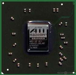
ATI's M82 GPU uses the TeraScale architecture and is made using a 55 nm production process at TSMC. With a die size of 67 mm² and a transistor count of 181 million it is a very small chip. M82 supports DirectX 10.1. For GPU compute applications, OpenCL version N/A can be used. It features 40 shading units, 4 texture mapping units and 4 ROPs.
Further reading:
R600 Series Instruction Set Architecture 
Graphics Processor
- Released
- Jan 7th, 2008
- GPU Name
- M82
- Desktop Variant
- RV620
- Codename
- Koopa
- Architecture
- TeraScale
- Foundry
- TSMC
- Process Size
- 55 nm
- Transistors
- 181 million
- Density
- 2.7M / mm²
- Die Size
- 67 mm²
- Package
- FCBGA-632/880
Graphics Features
- DirectX
- 10.1
- OpenGL
- 3.3
- OpenCL
- N/A
- Vulkan
- N/A
- Shader Model
- 4.1
- WDDM
- 1.1
- Compute
- GFX3
- DCE
- 3.0
- UVD
- 1.0
Render Config
- Shading Units
- 40
- TMUs
- 4
- ROPs
- 4
- Compute Units
- 2
- Vertex Cache
- 32 KB
- Texture Cache
- 32 KB
- Tex L1 Cache
- 32 KB per 4 SPs
- L2 Cache
- 64 KB
- Max. TDP
- 12 W
All TeraScale GPUs
- ATI M72
- ATI M74
- ATI M76
- ATI M82
- ATI M84
- ATI M86
- ATI M88
- ATI M92
- ATI M93
- AMD M93
- ATI M96
- ATI M97
- ATI M98
- ATI R600
- ATI R680
- ATI R700
- ATI RS780
- ATI RS880
- ATI RV610
- ATI RV620
- ATI RV630
- ATI RV635
- AMD RV670
- ATI RV670
- ATI RV710
- ATI RV711
- AMD RV711
- ATI RV730
- ATI RV740
- AMD RV770
- ATI RV770
- ATI RV790
- ATI RX881
- ATI Theater 650 PRO
- ATI Xenos Corona
- ATI Xenos Falcon
- ATI Xenos Jasper
- ATI Xenos Vejle
- ATI Xenos Xenon
ATI GPU Architecture History
Graphics cards using the ATI M82 GPU
| Name | Chip | Memory | Shaders | TMUs | ROPs | GPU Clock | Memory Clock |
|---|---|---|---|---|---|---|---|
| M82-SE | 256 MB | 40 | 4 | 4 | 450 MHz | 400 MHz | |
| 256 MB | 40 | 4 | 4 | 400 MHz | 400 MHz | ||
| M82-ME XT | 256 MB | 40 | 4 | 4 | 680 MHz | 400 MHz | |
| M82-SCE XT | 256 MB | 40 | 4 | 4 | 500 MHz | 400 MHz |


M82 GPU Notes
| Desktop Variant: RV620 Codename: Koopa Graphics/Compute: GFX3 Display Core Engine: 3.0 Unified Video Decoder: 1.0 Chip Codes: 216-0707001 - M82-S / M82-S XT 216-0707005 - M82-M / M82-M XT 216-0707007 - M82-SE 216-0707009 - M82-ME / M82-ME XT 216-0707011 - M82-SCE / M82-SCE XT 216-0707018 - M82-MPE 216-0707020 - M82-SE LP |
Sep 20th, 2024 21:01 EDT
change timezone
Latest GPU Drivers
New Forum Posts
- Next-Gen GPUs: What Matters Most to You? (59)
- TPU's Nostalgic Hardware Club (19008)
- Which RAM to choose for AMD 7950X3D and keep a 1:1 ratio (39)
- Horizon Zero Dawn Remastered: Speculation, Assumptions? (62)
- Game Not Launching (Windows 11, Nvidia Graphics) (1)
- Is Microsoft Deliberately Limiting AMD CPU Performance? (129)
- LG OLED club (34)
- It checks out as authentic (45)
- Free Games Thread (4049)
- Advise me before buying (48)
Popular Reviews
- Final Fantasy XVI Performance Benchmark Review - 35 GPUs Tested
- Fractal Design Era 2 Review
- TerraMaster F4-424 Review
- Warhammer: Space Marine 2 Performance Benchmark Review - 35 GPUs Tested
- HYTE Y70 Review
- Warhammer 40000: Space Marine 2 Handheld Performance Review
- Gigabyte C102 Glass Ice Review
- Upcoming Hardware Launches 2024 (Updated Jul 2024)
- Colorful iGame Loong Edition DDR5-7200 32 GB CL32 Review
- AMD Ryzen 9 9950X Review - The New Flagship
Controversial News Posts
- AMD Confirms Retreat from the Enthusiast GPU Segment, to Focus on Gaining Market-Share (255)
- Sony Reveals the PlayStation 5 Pro, Launches November 7th (179)
- AnandTech Shuts Down, an Icon of Tech News and Reviews Rides into the Sunset (151)
- AMD Ryzen Branch Prediction Optimizations Now Available to Windows 11 23H2 (131)
- Cyberpunk 2077 Update Adds AMD FSR 3 and Frame Generation for PC Players (120)
- AMD Ryzen 5 7600X3D Launched in the US as a MicroCenter-exclusive for $300, Part of a Bundle (116)
- Report: Intel Could Spin Out Foundry Business or Cancel Some Expansion Plans to Control Losses (113)
- NVIDIA's RTX 5060 "Blackwell" Laptop GPU Comes with 8 GB of GDDR7 Memory Running at 28 Gbps, 25 W Lower TGP (108)