Report an Error


ATI RV710

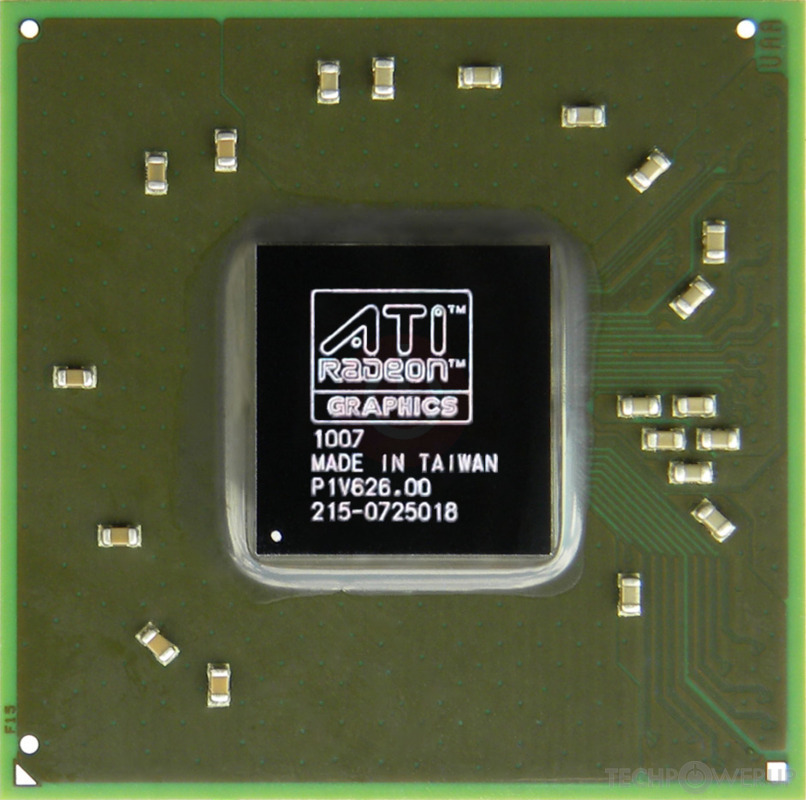
RV710

RV710
RV710 PCI

Block Diagram
ATI's RV710 GPU uses the TeraScale architecture and is made using a 55 nm production process at TSMC. With a die size of 73 mm² and a transistor count of 242 million it is a very small chip. RV710 supports DirectX 10.1 (Feature Level 10_1). For GPU compute applications, OpenCL version 1.1 can be used. It features 80 shading units, 8 texture mapping units and 4 ROPs.
Further reading:
R700 Series Instruction Set Architecture 
Graphics Processor
- Released
- Sep 30th, 2008
- GPU Name
- RV710
- Mobile Variant
- M92
- Codename
- Luigi
- Architecture
- TeraScale
- Foundry
- TSMC
- Process Size
- 55 nm
- Transistors
- 242 million
- Density
- 3.3M / mm²
- Die Size
- 73 mm²
- Package
- FCBGA-631
Graphics Features
- DirectX
- 10.1 (10_1)
- OpenGL
- 3.3
- OpenCL
- 1.1
- Vulkan
- N/A
- Shader Model
- 4.1
- WDDM
- 1.1
- Compute
- GFX3
- DCE
- 3.2
- UVD
- 2.2
Render Config
- Shading Units
- 80
- TMUs
- 8
- ROPs
- 4
- Compute Units
- 1
- Z-Stencil
- 4
- L1 Cache
- 16 KB per CU
- L2 Cache
- 64 KB
- Max. TDP
- 25 W
All TeraScale GPUs
- ATI M72
- ATI M74
- ATI M76
- ATI M82
- ATI M84
- ATI M86
- ATI M88
- ATI M92
- AMD M93
- ATI M93
- ATI M96
- ATI M97
- ATI M98
- ATI R600
- ATI R680
- ATI R700
- ATI RS780
- ATI RS880
- ATI RV610
- ATI RV620
- ATI RV630
- ATI RV635
- ATI RV670
- AMD RV670
- ATI RV710
- AMD RV711
- ATI RV711
- ATI RV730
- ATI RV740
- ATI RV770
- AMD RV770
- ATI RV790
- ATI RX881
- ATI Theater 650 PRO
- ATI Xenos Corona
- ATI Xenos Falcon
- ATI Xenos Jasper
- ATI Xenos Vejle
- ATI Xenos Xenon
ATI GPU Architecture History
Graphics cards using the ATI RV710 GPU
| Name | Chip | Memory | Shaders | TMUs | ROPs | GPU Clock | Memory Clock |
|---|---|---|---|---|---|---|---|
| RV710 HD4550 | 256 MB | 80 | 8 | 4 | 600 MHz | 655 MHz | |
| RV710 | 512 MB | 80 | 8 | 4 | 600 MHz | 650 MHz | |
| RV710 PCI | 512 MB | 80 | 8 | 4 | 600 MHz | 400 MHz | |
| RV710 | 512 MB | 80 | 8 | 4 | 600 MHz | 400 MHz | |
| RV710 | 512 MB | 80 | 8 | 4 | 600 MHz | 400 MHz | |
| RV710 | 1024 MB | 80 | 8 | 4 | 650 MHz | 500 MHz | |
| RV710 | 512 MB | 80 | 8 | 4 | 600 MHz | 400 MHz | |
| RV710 | 512 MB | 80 | 8 | 4 | 600 MHz | 400 MHz |


RV710 GPU Notes
| Mobile Variant: M92 Codename: Luigi Graphics/Compute: GFX3 Display Core Engine: 3.2 Unified Video Decoder: 2.2 |
May 2nd, 2024 19:50 EDT
change timezone
Latest GPU Drivers
New Forum Posts
- Have you got pie today? (16324)
- What's your latest tech purchase? (20414)
- Need help with a persistent infection possible rootkit or other device. (4)
- WCG Daily Numbers (12504)
- Milestones (13878)
- TPU's Rosetta Milestones and Daily Pie Thread (1867)
- PNY RTX 4070 Ti XLR8 OC - New worse BIOS/version? (105)
- What does Turbo Time Limit exactly mean? How often can a CPU go into turbo mode per timeslot? (0)
- PCIe 5.0 M.2 SSDs (35)
- 7800x3d $216 in bundle at Microcenter (23)
Popular Reviews
- Ugreen NASync DXP4800 Plus Review
- ASRock NUC BOX-155H (Intel Core Ultra 7 155H) Review
- Montech Sky Two GX Review
- HYTE THICC Q60 240 mm AIO Review
- Upcoming Hardware Launches 2023 (Updated Feb 2024)
- MOONDROP x Crinacle DUSK In-Ear Monitors Review - The Last 5%
- Team Group T-Force Vulcan ECO DDR5-6000 32 GB CL38 Review
- AMD Ryzen 7 7800X3D Review - The Best Gaming CPU
- Thermalright Phantom Spirit 120 EVO Review
- Meze Audio LIRIC 2nd Generation Closed-Back Headphones Review
Controversial News Posts
- Intel Statement on Stability Issues: "Motherboard Makers to Blame" (229)
- Windows 11 Now Officially Adware as Microsoft Embeds Ads in the Start Menu (165)
- Sony PlayStation 5 Pro Specifications Confirmed, Console Arrives Before Holidays (117)
- AMD's RDNA 4 GPUs Could Stick with 18 Gbps GDDR6 Memory (114)
- NVIDIA Points Intel Raptor Lake CPU Users to Get Help from Intel Amid System Instability Issues (106)
- AMD "Strix Halo" Zen 5 Mobile Processor Pictured: Chiplet-based, Uses 256-bit LPDDR5X (103)
- AMD Ryzen 9 7900X3D Now at a Mouth-watering $329 (103)
- TechPowerUp Hiring: Reviewers Wanted for Motherboards, Laptops, Gaming Handhelds and Prebuilt Desktops (93)