Report an Error


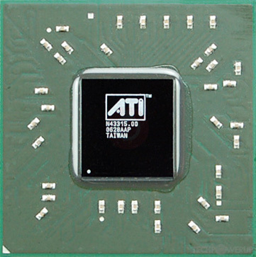
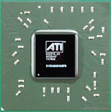
ATI RV530
RV530
RV530 PRO

RV530 X1650
ATI's RV530 GPU uses the Ultra-Threaded SE architecture and is made using a 90 nm production process at TSMC. With a die size of 150 mm² and a transistor count of 157 million it is a small chip. RV530 supports DirectX 9.0c (Feature Level 9_3). Modern GPU compute technologies are not available. It features 12 pixel shaders and 5 vertex shaders, 4 texture mapping units and 4 ROPs. Due to the lack of unified shaders you will not be able to run recent games at all (which require unified shader/DX10+ support).
Graphics Processor
- Released
- Oct 1st, 2005
- GPU Name
- RV530
- Mobile Variant
- M56 / M66
- Codename
- Jinn
- Architecture
- Ultra-Threaded SE
- Foundry
- TSMC
- Process Size
- 90 nm
- Transistors
- 157 million
- Density
- 1.0M / mm²
- Die Size
- 150 mm²
Graphics Features
- DirectX
- 9.0c (9_3)
- OpenGL
- 2.1
- OpenCL
- N/A
- Vulkan
- N/A
- Shader Model
- 3.0
- WDDM
- 1.0
- Compute
- GFX2
- DCE
- 1.0
Render Config
- Pixel Shaders
- 12
- Vertex Shaders
- 5
- TMUs
- 4
- ROPs
- 4
- Max. TDP
- 42 W
All Ultra-Threaded SE GPUs
ATI GPU Architecture History
Graphics cards using the ATI RV530 GPU
| Name | Chip | Memory | Shaders | TMUs | ROPs | GPU Clock | Memory Clock |
|---|---|---|---|---|---|---|---|
| RV530 PRO | 256 MB | 12 / 5 | 4 | 4 | 500 MHz | 390 MHz | |
| RV530 XT | 256 MB | 12 / 5 | 4 | 4 | 590 MHz | 690 MHz | |
| RV530 PRO | 256 MB | 12 / 5 | 4 | 4 | 500 MHz | 390 MHz | |
| 256 MB | 12 / 5 | 4 | 4 | 500 MHz | 400 MHz | ||
| RV530 PRO2 | 256 MB | 12 / 5 | 4 | 4 | 500 MHz | 400 MHz | |
| RV530 GL | 128 MB | 12 / 5 | 4 | 4 | 500 MHz | 500 MHz | |
| RV530 GL | 128 MB | 12 / 5 | 4 | 4 | 600 MHz | 700 MHz | |
| RV530 PRO2 | 256 MB | 12 / 5 | 4 | 4 | 500 MHz | 400 MHz | |
| RV530 X1650 | 256 MB | 12 / 5 | 4 | 4 | 500 MHz | 400 MHz | |
| 256 MB | 12 / 5 | 4 | 4 | 590 MHz | 690 MHz | ||
| RV530 LE | 256 MB | 12 / 5 | 4 | 4 | 587 MHz | 392 MHz | |
| RV530 XT2 | 256 MB | 12 / 5 | 4 | 4 | 600 MHz | 700 MHz |


RV530 GPU Notes
| Mobile Variant: M56 / M66 Codename: Jinn Graphics/Compute: GFX2 Display Core Engine: 1.0 Avivo Video Programmable pixel&vertex pipelines RV530 Chip Numbers: RV530 XT ES (215CACAKA13FG) |
May 1st, 2024 02:31 EDT
change timezone
Latest GPU Drivers
New Forum Posts
- What's an inexpensive AIO product line with a strong pump and low price? (89)
- 7900 XTX Seriously lacking (83)
- EK seems to be having major issues (70)
- RTX 4090? (34)
- Is this Sapphire PULSE RX 5600 XT legit or fake? (21)
- TPU Merch (11)
- Arctic MX-6 shelf life is just a couple months? (51)
- Brother bought a house, found some old PC hardware.. (15)
- The Official Thermal Interface Material thread (1117)
- RX580 2048SP 8GB Mllse (1)
Popular Reviews
- Ugreen NASync DXP4800 Plus Review
- Team Group T-Force Vulcan ECO DDR5-6000 32 GB CL38 Review
- HYTE THICC Q60 240 mm AIO Review
- Upcoming Hardware Launches 2023 (Updated Feb 2024)
- MOONDROP x Crinacle DUSK In-Ear Monitors Review - The Last 5%
- Thermalright Phantom Spirit 120 EVO Review
- AMD Ryzen 7 7800X3D Review - The Best Gaming CPU
- Montech Sky Two GX Review
- FiiO K19 Desktop DAC/Headphone Amplifier Review
- ASUS Radeon RX 7900 GRE TUF OC Review
Controversial News Posts
- Intel Statement on Stability Issues: "Motherboard Makers to Blame" (208)
- Windows 11 Now Officially Adware as Microsoft Embeds Ads in the Start Menu (156)
- Sony PlayStation 5 Pro Specifications Confirmed, Console Arrives Before Holidays (117)
- AMD's RDNA 4 GPUs Could Stick with 18 Gbps GDDR6 Memory (109)
- NVIDIA Points Intel Raptor Lake CPU Users to Get Help from Intel Amid System Instability Issues (106)
- AMD "Strix Halo" Zen 5 Mobile Processor Pictured: Chiplet-based, Uses 256-bit LPDDR5X (103)
- US Government Wants Nuclear Plants to Offload AI Data Center Expansion (98)
- TechPowerUp Hiring: Reviewers Wanted for Motherboards, Laptops, Gaming Handhelds and Prebuilt Desktops (90)