News Posts matching #AV1

Return to Keyword Browsing

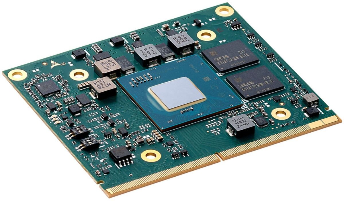
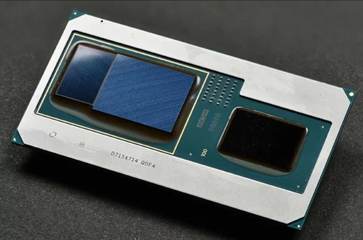
ADLINK Puts Intel Arc A-series GPUs on MXM Form Factor

After GUNNIR showed the same product back in January, ADLINK is now offering both Intel Arc A-series GPUs in MXM form factor. The MXM (Mobile PCI Express Module) is a standardized form factor that is used mostly in laptops and some small form factor PCs. Product pages confirm that ADLINK offers both the Intel Arc A370M and the Intel Arc A350M in MXM form factor.

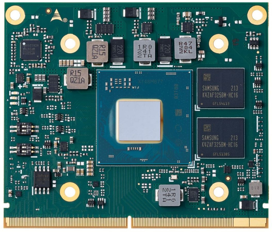
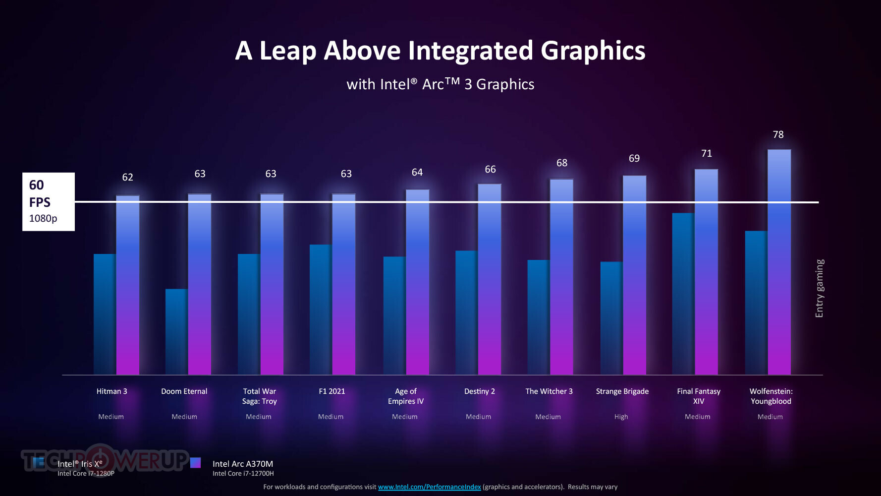
According to specifications The ADLINK MXM-AXe, as the product is called, is MXM 3.1 Type A based on Intel Arc GPU, packing 8 Xe-cores, 128 Execution Units, 4 GB of GDDR6 memory, and TDP of 35-50 W, which is pretty much standard for the Arc A370M GPU. The company also offers the same product with A350M GPU with TDP of 25-35 W. With decent power efficiency, full AV1 hardware encoding, and support for up to four 4K displays, such a GPU would be perfect for small form factor machines, and could be even a decent upgrade for some laptops.

Qualcomm Allegedly Preparing a Rival to Apple M SoC, Codenamed Hamoa

Qualcomm has been working on its Snapdragon SoCs for quite some time now, with massive success in the mobile phone space. However, the company's processors needed to be up to the task regarding laptops. For a user to not look at x86 offerings, the only remaining performant alternatives are Apple's M processors. In 2021 Qualcomm purchased the Nuvia team that was developing massively efficient and high-performance IP for laptops, similar to Apple M processors. Today, according to the insights from Kuba Wojciechowski (@Za_Raczke) on Twitter, we have some potential information about the upcoming Nuvia-powered SoC codenamed Hamoa.

According to the Twitter thread, Qualcomm's Hamoa processors are part of the Snapdragon 8xc Gen 4 compute platform and feature up to eight high-performance P-cores and four low-power E-cores, all based on Nuvia's IP. Allegedly the P-cores are being tested at 3.4 GHz, while the E-cores are tested at 2.5 GHz. The SoC splits CPU cores into blocks, each being a four-core group with 12 MB of shared L2 cache. There is also an 8 MB L3 cache structure; it needs to be clarified whether it is per core block or for the entire SoC. The chip employs 12 MB of system-level cache, with 4 MB of memory for graphics-related tasks handled by iGPU. The iGPU of choice is Adreno 740, with all modern APIs supported. Discrete graphics solutions are supported by the top-end SKUs, which allow eight PCIe 4.0 lanes to be directed toward dGPU, along with an additional four PCIe 4.0 lanes for NVMe SSD. For RAM, the chip uses up to 64 GBs of LPDDR5X eight-channel memory with up to 4.2 GHz speeds. Chip's media engines are structured to support decoding up to 4K120 and encode up to 4K60 with AV1.

AMD Ryzen 7040 Series "Phoenix Point" Mobile Processor I/O Detailed: Lacks PCIe Gen 5

The online datasheets of some of the first AMD Ryzen 7040 series "Phoenix Point" mobile processors went live, detailing the processor's I/O feature-set. We learn that AMD has decided to give PCI-Express Gen 5 a skip with this silicon, at least in its mobile avatar. The Ryzen 7040 SoC puts out a total of 20 PCI-Express Gen 4 lanes, all of which are "usable" (i.e. don't count 4 lanes toward chipset-bus). This would mean that the silicon has a full PCI-Express 4.0 x16 interface for discrete graphics, and a PCI-Express 4.0 x4 link for a CPU-attached M.2 NVMe slot; unlike the "Raphael" desktop MCM and the "Dragon Range" mobile MCM, whose client I/O dies put out a total of 28 Gen 5 lanes (24 usable, with x16 PEG + two x4 toward CPU-attached M.2 slots).

Another interesting aspect about "Phoenix Point" is its memory controllers. The SoC features a dual-channel (four sub-channel) DDR5 memory interface, besides support for LPDDR5 and LPDDR5x. DDR5-5600 and LPDDR5-7600 are the native speeds supported. What's really interesting is the maximum amount of memory supported, which stands at 256 GB—double that of "Raphael" and "Dragon Range," which top out at 128 GB. This bodes well for the eventual Socket AM5 APUs AMD will design based on the "Phoenix Point" silicon. Older Ryzen 5000G "Cezanne" desktop APUs are known for superior memory overclocking capabilities to 5000X "Vermeer," with the monolithic nature of the silicon favoring latencies. Something similar could be expected from "Phoenix Point."

MediaTek Expands IoT Platform with Genio 700 for Industrial and Smart Home Products

Ahead of CES 2023, MediaTek today announced the latest chipset in the Genio platform for IoT devices, the octa-core Genio 700 designed for smart home, smart retail, and industrial IoT products. The new chipset will be featured as part of a demo at MediaTek's booth at CES 2023. With a focus on power efficiency, the MediaTek Genio 700 is a N6 (6 nm) IoT chipset that boasts two ARM A78 cores running at 2.2 GHz and six ARM A55 cores at 2.0 GHz while providing 4.0 TOPs AI accelerator. It comes with support for FHD 60p + 4K 60p display, as well as an ISP for better images.

"When we launched the Genio family of IoT products last year, we designed the platform with the scalability and development support that brands need, paving the way for opportunities to continue expanding," said Richard Lu, Vice President of MediaTek IoT Business Unit. "With a focus on industrial and smart home products, the Genio 700 is a perfect natural addition to the lineup to ensure we can provide the widest range of support possible to our customers."

Khronos Finalizes Vulkan Video Extensions for Accelerated H.264 and H.265 Decode

In April 2021, the Vulkan Working Group at Khronos released a set of provisional extensions, collectively called "Vulkan Video," for seamlessly integrating hardware-accelerated video compression and decompression into the Vulkan API. Today, Khronos is releasing finalized extensions that incorporate industry feedback and expose core and decode Vulkan Video functionality to provide fully accelerated H.264 and H.265 decode.

Khronos will release an ongoing series of Vulkan Video extensions to enable additional codecs and accelerated encode as well as decode. This blog is a general overview of the Vulkan Video architecture and also provides details about the finalized extensions and links to important resources to help you create your first Vulkan Video applications.

New Intel oneAPI 2023 Tools Maximize Value of Upcoming Intel Hardware

Today, Intel announced the 2023 release of the Intel oneAPI tools - available in the Intel Developer Cloud and rolling out through regular distribution channels. The new oneAPI 2023 tools support the upcoming 4th Gen Intel Xeon Scalable processors, Intel Xeon CPU Max Series and Intel Data Center GPUs, including Flex Series and the new Max Series. The tools deliver performance and productivity enhancements, and also add support for new Codeplay plug-ins that make it easier than ever for developers to write SYCL code for non-Intel GPU architectures. These standards-based tools deliver choice in hardware and ease in developing high-performance applications that run on multiarchitecture systems.

"We're seeing encouraging early application performance results on our development systems using Intel Max Series GPU accelerators - applications built with Intel's oneAPI compilers and libraries. For leadership-class computational science, we value the benefits of code portability from multivendor, multiarchitecture programming standards such as SYCL and Python AI frameworks such as PyTorch, accelerated by Intel libraries. We look forward to the first exascale scientific discoveries from these technologies on the Aurora system next year."
-Timothy Williams, deputy director, Argonne Computational Science Division

FFmpeg Gets NVENC AV1 Encode Support for a 75-100% Encoding Speed Uplift Over HEVC

Popular video transcoding and playback software FFmpeg, in its latest update, received support for AV1 format hardware-accelerated encoding leveraging the NVENC AV1 hardware encoders on the latest NVIDIA GeForce RTX 40-series "Ada" GPUs. The author Timo Rothenpieler remarked that in his testing, the new NVENC AV1 encoder is outperforming the NVENC HEVC-based FFmpeg encoding by 75 to 100 percent, in terms of encoding speed, at comparable quality. When deployed at a data-center scale, or even a production studio-scale, accelerated AV1 encoding should have a tangible impact on costs, and not just because AV1 is a royalty-free format. NVENC AV1 encoding support was also recently added to OBS Studio, the popular free video streaming software.

AMD Announces the $999 Radeon RX 7900 XTX and $899 RX 7900 XT, 5nm RDNA3, DisplayPort 2.1, FSR 3.0 FluidMotion

AMD today announced the Radeon RX 7900 XTX and Radeon RX 7900 XT gaming graphics cards debuting its next-generation RDNA3 graphics architecture. The two new cards come at $999 and $899—basically targeting the $1000 high-end premium price point.
Both cards will be available on December 13th, not only the AMD reference design, which is sold through AMD.com, but also custom-design variants from the many board partners on the same day. AIBs are expected to announce their products in the coming weeks.

The RX 7900 XTX is priced at USD $999, and the RX 7900 XT is $899, which is a surprisingly small difference of only $100, for a performance difference that will certainly be larger, probably in the 20% range. Both Radeon RX 7900 XTX and RX 7900 XT are using the PCI-Express 4.0 interface, Gen 5 is not supported with this generation. The RX 7900 XTX has a typical board power of 355 W, or about 95 W less than that of the GeForce RTX 4090. The reference-design RX 7900 XTX uses conventional 8-pin PCIe power connectors, as would custom-design cards, when they come out. AMD's board partners will create units with three 8-pin power connectors, for higher out of the box performance and better OC potential. The decision to not use the 16-pin power connector that NVIDIA uses was made "well over a year ago", mostly because of cost, complexity and the fact that these Radeons don't require that much power anyway.

OBS Studio 28.1 Released with Support for NVENC AV1 Accelerated Encoding on Ada GPUs

Popular video streaming software suite OBS Studio, in its latest version 28.1 release, adds hardware-accelerated AV1 encoding support for NVIDIA GeForce RTX 40-series "Ada" GPUs. This takes advantage of the updated NVENC hardware media encoders "Ada" comes with, which has fixed-function hardware to encode AV1 video, a royalty-free format that offers comparable quality and bitrates to HEVC. There are a handful limitations, besides the fact that this only works with the RTX 40-series. To begin with, only the NV12 (OBS default) and P010 color formats are supported. The "rescale" feature in advanced output modes, isn't supported for now. Grab OBS Studio from the link below.

DOWNLOAD: OBS Studio 28.1

Restoring the Balance: Intel Arc A750 & A770 Performance per Dollar Detailed, available Oct 12th

It's the moment you've been waiting for! (And the moment our teams have been working towards!) The Intel Arc A750 and A770 GPUs will be for sale on October 12th starting at $289 and $329 respectively, with the Arc A770 Limited Edition available for $349. After years of price increases in the massive $200-400 GPU segment, Intel is bringing balance back to the GPU market. Pricing seems to have gone off the deep end and we're working to reel it back in with the Intel Arc A-series GPUs. As we've shown in earlier performance blogs, the Arc A750 and A770 trade blows with the NVIDIA GeForce RTX 3060—a popular mainstream GPU. Intel CEO Pat Gelsinger called out the extreme GPU prices in his Intel Innovation Day 1 keynote, showing that the last four years have seen a nonstop upward trend in prices of mainstream GPUs. By entering the GPU space as a third player, Intel is ready to turn these tides in gamers' favor and disrupt the market.

On average, a new GeForce RTX 3060 will set you back $418. (This number was calculated on Newegg.com, targeting in stock, sold by Newegg, new RTX 3060 cards as of Sept 22, 2022.) Picking up an Intel Arc A750 on October 12th for $289 gets you 53% more performance per dollar on average, or an 8 GB Arc A770 for $329 provides 42% more perf/dollar. Why is that? The Arc A700-series performance beats the 3060 in most modern titles using DirectX 12 or Vulkan APIs and our GPUs aren't far behind in most DX11 games—all for much less cash.

NVIDIA Ada AD102 Block Diagram and New Architectural Features Detailed

At the heart of the GeForce RTX 4090 is the gigantic AD102 silicon, which we broadly detailed in an older article. Built on the 4 nm silicon fabrication process, this chip measures 608 mm² in die-area, and crams in 76.3 billion transistors. We now have our first look into the silicon-level block diagram of the AD102, including the introduction of several new components.

The AD102 features a PCI-Express 4.0 x16 host interface, and a 384-bit GDDR6X memory interface. The Gigathread Engine acts as a the main resource allocation component of the silicon. Ada introduces the Optical Flow Accelerator, a component crucial for DLSS 3 to generate entire frames without involving the graphics rendering machinery. The chip features double the number of media-encoding hardware engines as "Ampere," including hardware-accelerated AV1 encode/decode. Multiple accelerators mean that multiple streams of videos can be transcoded (helpful in a media production environment), or transcoding is performed at twice the FPS rate (each encoder takes turns at encoding a single frame).

Intel Data-Center GPU Flex Series "Arctic Sound-M" Launched: Visual Processing, Media, and Inference top Applications

Intel today launched its Arctic Sound M line of data-center GPUs. These are not positioned as HPC processors like the "Ponte Vecchio," but GPUs targeting cloud-compute providers, with their main applications being in the realm of visual processing, media, and AI inferencing. Their most interesting aspect has to be the silicon, which are the same 6 nm "ACM-G11" and "ACM-G10" chips powering the Arc "Alchemist" client graphics cards, based on the Xe-HPG architecture. Even more interesting is their typical board power values, ranging between 75 W to 150 W. The cards are built in the PCI-Express add-on card form-factor, with their cooling solutions optimized for rack airflow.

The marketing name for these cards is simply Intel Data Center GPU Flex, with two models being offered: The Data Center GPU Flex-140, and Flex-170. The Flex-170 is a full-sized add-on card based on the larger ACM-G10 silicon, which has 32 Xe Cores (4,096 unified shaders), whereas the Flex-140, interestingly, is a low-profile dual-GPU card with two smaller ACM-G11 chips that each has 8 Xe Cores (1,024 unified shaders). The two chips appear to be sharing a PCIe bridge chip in the renders. Both models come with four Xe Media Engines that pack AV1 encode hardware-acceleration, XMX AI acceleration, real-time ray tracing, and GDDR6 memory.

Intel Unveils Arc Pro Graphics Cards for Workstations and Professional Software

Intel has today unveiled another addition to its discrete Arc Alchemist graphics card lineup, with a slight preference to the professional consumer market. Intel has prepared three models for creators and entry pro-vis solutions, called Intel Arc Pro graphics cards. All GPUs are AV1 accelerated, have ray tracing support, and are designed to handle AI acceleration inside applications like Adobe Premiere Pro. At the start, we have a small A30M mobile GPU aimed at laptop designs. It has a 3.5 TeraFLOP FP32 capability inside a configurable 35-50 Watt TDP envelope, has eight ray tracing cores, and 4 GB of GDDR6 memory. Its display output connectors depend on OEM's laptop design.

Next, we have the Arc A40 Pro discrete single-slot GPU. Having 3.5 TeraFLOPs of FP32 single-precision performance, it has eight ray tracing cores and 6 GB of GDDR6 memory. The listed maximum TDP for this model is 50 Watts. It has four mini-DP ports for video output, and it can drive two monitors at 8K 60 Hz, one at 5K 240 Hz, two at 5K 120 Hz, or four at 4K 60 Hz refresh rate. Its bigger brother, the Arc A50 Pro, is a dual-slot design with 4.8 TeraFLOPs of single-precision FP32 computing, has eight ray tracing cores, and 6 GB of GDDR6 memory as well. It has the same video output capability as the Arc A40 Pro, with a beefier cooling setup to handle the 75 Watt TDP. All software developed using the OneAPI toolkit can be accelerated using these GPUs. Intel is working with the industry to adapt professional software for Arc Pro graphics.

Intel Arc A380 Desktop Graphics Card Launched in China at $153 (equivalent)

Intel officially launched the Arc A380 "Alchemist" entry-mainstream desktop graphics card in China, priced at RMB ¥1,030, including VAT, which roughly converts to USD $153. The Arc A380 "Alchemist" is based on the Xe-HPG graphics architecture, and the smaller DG2-128 (ACM-G11) silicon, which is built on the TSMC N6 (6 nm) silicon fabrication process.

The A380 desktop GPU is endowed with 8 Xe Cores, or 128 EU (execution units), which work out to 1,024 unified shaders. The chip features a 96-bit wide GDDR6 memory interface, running 6 GB of memory. Despite these hardware specs, you get full DirectX 12 Ultimate capability, including ray tracing, and the XeSS performance enhancement. There are also several content-creation accelerators, including Intel XMX, and AV1 hardware-encode capabilities.

Intel "Arctic Sound M" Enterprise Accelerator Shown Encoding AV1 Video

Intel showed off the video encode acceleration capabilities of its upcoming Data Center GPU codenamed "Arctic Sound M," which features AV1 video encode hardware-acceleration. Intel has been pushing for AV1 to be adopted as the streaming video standard for some years now, as it offers comparable bitrate savings and quality to H.265, but is royalty free, resulting in tens of millions of Dollars of royalty savings for streaming content providers such as Netflix, as well as consumer electronics manufacturers, particularly smart TV makers.

Intel's accelerator is a single-slot, full-height add-on card with a PCI-Express x16 interface. It relies on rack airflow for cooling, and features a metal-channel heatsink. Power is drawn from a single 8-pin PCIe power connector. There are no encoding performance numbers put out, except the 30% bitrate savings AV1 offers compared to the current industry standard, H.264. This 30% saving adds up in a big way for a streaming content provider.
Intel's video presentation follows.

Moore Threads Unveils MTT S60 & MTT S2000 Graphics Cards with DirectX Support

Chinese company Moore Threads has unveiled their MTT GPU series just 18 months after the company's establishment in 2020. The MT Unified System Architecture (MUSA) architecture is the first for any Chinese company to be developed fully domestically and includes support for DirectX, OpenCL, OpenGL, Vulkan, and CUDA. The company announced the MTT S60 and MTT S2000 single slot desktop graphics cards for gaming and server applications at a recent event. The MTT S60 is manufactured on a 12 nm node and features 2,048 MUSA cores paired with 8 GB of LPGDDR4X memory offering 6 TFLOPs of performance. The MTT S2000 is also manufactured on a 12 nm node and doubles the number of MUSA cores to 4096 paired with 32 GB of undisclosed video memory allowing it to reach 12 TFLOPs.

Moore Threads joins Intel in supporting AV1 encoding on a consumer GPU with MUSA cards featuring H.264, H.265, and AV1 encoding support in addition to H.264, H.265, AV1, VP8, and VP9 decoding. The company is also developing a physics engine dubbed Alphacore which is said to work with existing tools such as Unity, Unreal Engine, and Houdini to accelerate physics performance by 5 to 10 times. The only gaming performance shown was a simple demonstration of the MTT S60 running League of Legends at 1080p without any frame rate details.

Intel Formally Announces Arc A-series Graphics

For decades, Intel has been a champion for PC platform innovation. We have delivered generations of CPUs that provide the computing horsepower for billions of people. We advanced connectivity through features like USB, Thunderbolt and Wi-Fi. And in partnership with the PC ecosystem, we developed the ground-breaking PCI architecture and the Intel Evo platform, pushing the boundary for what mobile products can do. Intel is uniquely positioned to deliver PC platform innovations that meet the ever-increasing computing demands of professionals, consumers, gamers and creators around the world. Now, we take the next big step.

Today, we are officially launching our Intel Arc graphics family for laptops, completing the Intel platform. These are the first discrete GPUs from our Intel Arc A-Series graphics portfolio for laptops, with our desktop and workstation products coming later this year. You can visit our Newsroom for our launch video, product details and technical demos, but I will summarize the highlights of how our Intel Arc platform and A-Series mobile GPU family will deliver hardware, software, services and - ultimately - high-performance graphics experiences.

Intel Introduces Arctic Sound-M Data Center Graphics Card Based on DG2 Design and AV1 Encoding

At Intel's 2022 investor meeting, the company has presented a technology roadmap update to give its clients an insight into what is to come. Today, team blue announced one of the first discrete data-centric graphics cards in the lineup, codenamed Arctic Sound-M GPU. Based on the DG2 Xe-HPG variation of Intel Xe GPUs, Arctic Sound-M is the company's first design to enter the data center space. The DG2 GPU features 512 Execution Units (EUs), which get passive cooling from the single-slot design of Arctic Sound's heatsink, envisioned for data center enclosures with external airflow.

One of the most significant selling points that Intel advertises is support for hardware-based AV1 encoding standard. This feature allows the card to achieve a 30% greater bandwidth, and it is the main differentiator between consumer-oriented Arc Alchemist GPUs and itself. The card is powered by PCIe power and an 8-pin EPS power connector. Arctic Sound-M is already sampling to select customers and it will become available in the middle of 2022.

Below is Intel's teaser video.

Intel Updates Technology Roadmap with Data Center Processors and Game Streaming Service

At Intel's 2022 Investor Meeting, Chief Executive Officer Pat Gelsinger and Intel's business leaders outlined key elements of the company's strategy and path for long-term growth. Intel's long-term plans will capitalize on transformative growth during an era of unprecedented demand for semiconductors. Among the presentations, Intel announced product roadmaps across its major business units and key execution milestones, including: Accelerated Computing Systems and Graphics, Intel Foundry Services, Software and Advanced Technology, Network and Edge, Technology Development, More: For more from Intel's Investor Meeting 2022, including the presentations and news, please visit the Intel Newsroom and Intel.com's Investor Meeting site.

AMD Ryzen 6000 "Rembrandt" Mobile Processors Pack Next-Gen Connectivity: Leak

AMD is planning to crash Intel's big 12th Gen Core "Alder Lake-P" mobile processor launch with its own next-gen launch, the Ryzen 6000 mobile processor series. These chips are the company's first built on the TSMC N6 (6 nm) silicon fabrication process, and combine up to 8 "Zen 3+" CPU cores, with a next-generation iGPU based on the RDNA2 graphics architecture. The company has given the Media CoreNext and Video CoreNext engines incremental updates, according to a leaked slide scored by VideoCardz.

Ryzen 6000 "Rembrandt" processors come with hardware-accelerated decode of the AV1 video format. The Display CoreNext (display I/O engine) now supports DisplayPort 2.0, complete with DSC, UHBR10, HDR10+, and variable refresh-rate. The HDR pipeline has awareness for the various display panel types, including OLED and mini-LED. The iGPU on "Rembrandt" features up to 12 compute units (768 stream processors). It remains to be seen if Ray Accelerators are featured, as that would make this the first iGPU (on the PC platform) with DirectX 12 Ultimate support.

MediaTek's Pentonic 2000 is World's first TV SoC with H.266 support

With ever increasing computational needs from TV SoCs, as we're moving towards higher resolutions and refresh rates, MediaTek is getting ready for the next generation of 8K TVs with its new Pentonic 2000 SoC. This is the world's first TV SoC to support the new H.266 video codec standard, which is an evolution of the H.265 intended for 8K content.

The Pentonic 2000 is fabbed using TSMC's N7 node and it's the first commercial TV SoC to be made on this manufacturing process according to MediaTek. The SoC supports 8K resolution content at up to 120 Hz with MEMC (Motion Estimation, Motion Compensation) and has an integrated AI engine to help improve scaling from lower resolutions. MediaTek also claims that the Pentonic 2000 features the "industry's most powerful CPU and GPU" in a smart TV SoC, without giving away any actual details, although it the SoC does support UFS 3.1 storage, which suggests that we're looking at a recent Arm Cortex-A7x based SoC at the very least.

First AMD Radeon Vega M Drivers for Intel NUC8i7HNK and NUC8i7HVK in Over 16 Months Released

Intel and AMD released the first Radeon Software drivers for the exotic Radeon Vega M graphics found in Intel NUC8i7HNK and NUC8i7HVK, in over 16 months. The Intel Download Center just added version 21.10.03.11 of Radeon Software for the graphics solution, dated 09/09/2021. The previous drivers dated all the way back to February 2020, and were based on Adrenalin 20.2.

The drivers are based on a release candidate of Adrenalin 21.10, which is 21.10RC1, but does not include the security updates AMD could be bundling with the upcoming 21.10 drivers (October 2021). "Radeon RX Vega M Graphics Driver version 21.10.03.11, which is based on 21.10RC1, does not include the latest functional and security updates. An update is targeted to be released in March of 2022 and will include additional functional and security updates. Customers should update to the latest version as it becomes available," says Intel in the release notes of the drivers. The drivers do include optimization for the latest games, including "Metro Exodus" (DX12), and "Resident Evil Village," besides adding support for Microsoft PlayReady AV1 decode.

DOWNLOAD: AMD Radeon Vega M drivers for Intel NUC8i7HNK and NUC8i7HVK from Intel

AMD Releases Radeon Software Adrenalin 21.4.1 WHQL with Dozens of New Features

AMD today released the Radeon Software Adrenalin 21.4.1 drivers, which introduce major updates to the soft-product that completes your AMD Radeon graphics cards. The drivers come with updates to the Radeon Software interface, and the AMD Link remote-gameplay utility. Radeon Software now comes with an improved installer with installation presets that let you choose between a Full (typical) installation, with all software features installed; a Minimal installation with an interface that only has basic settings related to the display and GPU; and "driver-only" that only installs the display driver, and no additional software.

There are several new features introduced within Radeon Software. Vivid Gaming Display Color Enhancement is a new monitor color profile that enables a more "vivid" color palette that lets you liven up "color deficient" scenes. The interface lets you take control of protanopia, deuteranopia, and tritanopia components of the color. The search bar that lets you dig through the hundreds of features, has been improved. There are many other minor UI improvements, such as stats in the Games tab, a toggle for the in-built web-browser, and global controls for the hotkeys.

DOWNLOAD: AMD Radeon Software Adrenalin 21.4.1

NVIDIA Updates Video Encode and Decode Matrix with Reference to Ampere GPUs

NVIDIA has today updated its video encode and decode matrix with references to the latest Ampere GPU family. The video encode/decode matrix represents a table of supported video encoding and decoding standards on different NVIDIA GPUs. The matrix has a reference dating back to the Maxwell generation of NVIDIA graphics cards, showing what video codecs are supported by each generation. That is a useful tool for reference purposes, as customers can check if their existing or upcoming GPUs support a specific codec standard if they need any for video reproduction purposes. The update to the matrix comes in a form of Ampere GPUs, which are now present there.

For example, the table shows that, while supporting all of the previous generations of encoding standards, the Ampere based GPUs feature support for HEVC B Frame standard. For decoding purposes, the Ampere lineup now includes support for AV1 8-bit and 10-bit formats, while also supporting all of the previous generation formats. For a more detailed look at the table please go toNVIDIA's website here.
NVIDIA Encoding and Decoding Standards

AMD RDNA2 Graphics Architecture Features AV1 Decode Hardware-Acceleration

AMD's RDNA2 graphics architecture features hardware-accelerated decoding of the AV1 video format, according to a Microsoft blog announcing the format's integration with Windows 10. The blog mentions the three latest graphics architectures among those that support accelerated decoding of the format—Intel Gen12 Iris Xe, NVIDIA RTX 30-series "Ampere," and AMD RX 6000-series "RDNA2." The AV1 format is being actively promoted by major hardware vendors to online streaming content providers, as it offers 50% better compression than the prevalent H.264 (translating into that much bandwidth savings), and 20% better compression than VP9. You don't need these GPUs to use AV1, anyone can use it with Windows 10 (version 1909 or later), by installing the AV1 Video Extension from the Microsoft Store. The codec will use software (CPU) decode in the absence of hardware acceleration.
Return to Keyword Browsing
May 16th, 2024 06:31 EDT change timezone

New Forum Posts

Popular Reviews

Controversial News Posts