Wednesday, April 21st 2010

Intel Sandy Bridge to Introduce New Sockets, Chipsets, Reorganize Platform Further
Intel plans a pair of new sockets for launch with its new processor architecture that succeeds Westmere, codenamed "Sandy Bridge", which are due for 2011. As part of its "tick-tock" product launch strategy, the company is currently transitioning between the 45 nm "tock" (Nehalem architecture), and 32 nm "tick" (Westmere architecture). In 2011, it will transition from the 32 nm "tick" (Westmere architecture), to the 32 nm "tock" (Sandy Bridge architecture). The company uses a "tick-tock" model of process development, where each processor architecture gets to be made in two successive manufacturing processes, while each process gets to build two succeeding architectures. It seems to have become clear that with Sandy Bridge, Intel will also switch to new socket designs, making existing motherboards obsolete then. Architecturally, Sandy Bridge will introduce new feature-sets that make the CPU more powerful, clock-to-clock, such as AVX - Advanced Vector Extensions, an evolution of the SSE instruction set, native AES engine which has been introduced with Westmere, and so on.
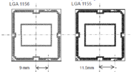
The present LGA-1156 package on which Intel builds value-through-performance processors including a bulk of mainstream processors, will be succeeded with the LGA-1155 package. Though similar, LGA-1155 and LGA-1156 are not inter-compatible, meaning that LGA-1155 processors will not work on existing LGA-1156 motherboards, and LGA-1156 processors will not work on LGA-1155 motherboards, either. For these processors, the arrangement of vital components is similar to the LGA-1156 package, except that every LGA-1155 processor - dual-core or quad-core - will feature an on-die display controller.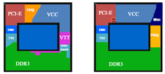 The die itself will be monolithic, where the northbridge component completely integrates with the processor component, leaving only the southbridge outside the package, on the motherboard. Currently, the "Clarkdale" and "Arrandale" dual-core processors have the processor and northbridge components on separate dies, but on the same package. LGA-1155 is also designated as socket H2 (LGA-1156 is H1), the package is identical in size to LGA-1156, but has a different pin layout and orientation notch.
Chipsets that drive the LGA-1156 platform include P67, H67, H61, and Q67, which will support features which were conceived prior to Ibex Peak platform's launch, but were shelved, such as ONFI NAND Flash "Braidwood", etc. USB 3.0 still isn't part of the feature-set, though native SATA 6 Gb/s support is on the cards.
The next big platform to succeed the LGA-1366, which caters to processors in the upper performance-though-enthusiast segments is the "Patsburg" platform, succeeding the existing "Tylersburg" based Intel X58, 5000 series chipsets. Here, Intel will introduce a massive new socket, the LGA-2011. The pin count is drastically increased for two reasons: the processor will have a 256-bit wide memory interface (quad-channel DDR3), and the northbridge component (currently X58 PCH) will be integrated completely into the processor package, upping the pin count with the PCI-Express and DMI pins. The on-die PCI-Express 2.0 root-complex will give out 32 lanes for graphics (unlike 16 lanes on the LGA-1155), and a DMI link to the so-called "Intel X68" chipset, which is relegated to being a Platform Controller Hub, just like the P55, or P67. The X68 could have a feature-set similar to the P67.
Source:
bit-tech.net
The present LGA-1156 package on which Intel builds value-through-performance processors including a bulk of mainstream processors, will be succeeded with the LGA-1155 package. Though similar, LGA-1155 and LGA-1156 are not inter-compatible, meaning that LGA-1155 processors will not work on existing LGA-1156 motherboards, and LGA-1156 processors will not work on LGA-1155 motherboards, either. For these processors, the arrangement of vital components is similar to the LGA-1156 package, except that every LGA-1155 processor - dual-core or quad-core - will feature an on-die display controller.
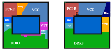

The next big platform to succeed the LGA-1366, which caters to processors in the upper performance-though-enthusiast segments is the "Patsburg" platform, succeeding the existing "Tylersburg" based Intel X58, 5000 series chipsets. Here, Intel will introduce a massive new socket, the LGA-2011. The pin count is drastically increased for two reasons: the processor will have a 256-bit wide memory interface (quad-channel DDR3), and the northbridge component (currently X58 PCH) will be integrated completely into the processor package, upping the pin count with the PCI-Express and DMI pins. The on-die PCI-Express 2.0 root-complex will give out 32 lanes for graphics (unlike 16 lanes on the LGA-1155), and a DMI link to the so-called "Intel X68" chipset, which is relegated to being a Platform Controller Hub, just like the P55, or P67. The X68 could have a feature-set similar to the P67.
119 Comments on Intel Sandy Bridge to Introduce New Sockets, Chipsets, Reorganize Platform Further
On applications that aren't heavily multithreaded, the architecture of Core i# is inferior to that of Core 2 and Phenom II.[/QUOTE]
No. Core i7 is faster in single threaded application. It has higher performance per clock than any other architecture. Look at how it fares in gaming compared to phenom and Core 2 Quads.
Look here at the bottom www.anandtech.com/bench/Product/45?vs=48
Two games are tied, two games where either or wins. That sums up the whole of the video game comparison... it's even.
This is a bad financial move for intel. Exactly like the ps3 was for sony.
Look at the most to least portion of the results here:
forums.techpowerup.com/showpost.php?p=1686222&postcount=119
4 times was exagerating :roll:, it was (as expected) almost twice as fast with hyperthreading enabled. No hyperthreading = very low scores except in the floating point department. It got hurt very badly in the integer department without Hyperthreading. That proves that over half of the ALU's are idle without two threads throwing work at it where the FPUs are mostly loaded with just a single thread giving it work.
As you can see, I haven't done any testing at only one thread yet.Phenoms II win 50% of the time. Core 2 loses all the time because of the delay in reaching the RAM that is minimized in Phenom II and Core i#.
uint64: Core i7 920 < Phenom II 955
double: Core i7 920 > Phenom II 955 (not by much on the 4 thread test)
Core i7 920 is better at floating point operations than the Phenom II 955 but not at integer operations. If you are testing with an application that is heavy in floats, the Core i7 will come out on top (with hypthreading disabled). If the application is heavy on ints, Core i7 (hyperthreading disabled) will come in second.
Turning on hyperthreading and the workload the same (4 threads each), Phenom II 955 and Core i7 920 are very close (i7 on top) while the Core i7 920 slaughters the Phenom II 955 in the floating point area. Turn on hyperthreading and add 4 more threads and the Core i7 920 simply mocks the Phenom II 955.Read the results at the bottom for analysis. The test was to compare HT to no HT, two processors versus one, and AMD versus Intel (they were about the same price when the benchmark was done).
When I first wrote it, it was when P4s were all big and I made it to compare them. I first wrote it on my P4 2.4GHz Northwood and since then I have been using it on all the CPUs I have had since and here are some quick results:
And if you look back at history these scores really do correlate well. K7 was faster than Netburst per clock, Pentium M was much faster than Netburst, Core was faster still. Nehalem gets the highest score therefore Nehalem is the best.
Anyone who doubts these findings are either a fanboy or a just plain stupid.
Oh this is a rewrite of the original program for P4s.
Let me know what you get.
Edit* I got 11468
What type of calculations does this appication do? Lemme guess, floating point?According to that, Phenom II 965 BE and Core 2 Q9650 are well matched, Core 2 being slightly more efficient clock for clock.
I don't think my program is affected by memory much, hence the very low difference.