News Posts matching #Sandy Bridge

Return to Keyword Browsing

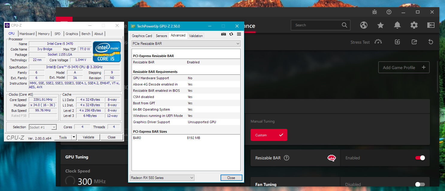
ReBarUEFI is a Boot Time Module that Enables Resizable BAR on Some Older Platforms

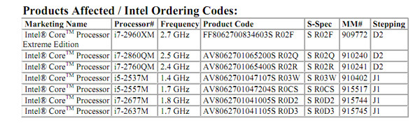
Officially, support for resizable BAR on the Intel platform begins with the 10th Gen Core "Comet Lake," and for AMD, the Ryzen 3000 "Zen 2." It is a PCI-SIG feature that allows the software to see the entire amount of video memory on your graphics card as a single contiguous addressable block, rather than through 256 MB apertures—a workaround for the original PCI Express specification as the industry was transitioning to it from AGP. The PCI-SIG had introduced resizable BAR way back during the PCI-Express 2.0 specification (late 2000s), although none of the GPU or platform vendors of the time bothered to implement it. Resizable BAR is known to have a positive impact on performance for modern GPUs from NVIDIA and AMD; although its most profound performance impact is on the Intel Arc "Alchemist" GPUs, which suffer a large performance penalty without it.

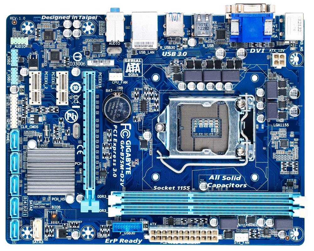
ReBarUEFI by xCuri0 is a UEFI DXE driver mod, which requires you to know how to modify the UEFI firmware of your motherboard. The ReBarUEFI mod calls for a motherboard that implements UEFI, the older legacy BIOS won't do. The industry transitioned to UEFI in the early 2010s, roughly around the time of Intel "Sandy Bridge." UEFI DXE drivers provide basic support for the various hardware on your system. The ReBarUEFI driver informs software that the platform is capable of resizable BAR. Some motherboards may require you to enable the "Above 4G Decode" setting. The author claims that users on platforms as old as 2nd Gen Core "Sandy Bridge" have had success in getting resizable BAR to work.

Microsoft Releases Microcode Updates Adressing Intel CPU Vulnerabilities under Windows 10

Microsoft today has released several microcode updates for Intel CPUs. The updates are meant to be applied in a case-by-case basis under their Windows 10 operating system, and these updates target several releases of that OS (ranging from version 1507 through version 1903/1909). These address several vulnerability exploits related to side-channel and speculative execution attacks on Intel CPUs.

The updates need to be installed specifically for the Windows OS version you're rocking, and on systems with CPUs affected by the vulnerabilities and covered by this microcode update release. These include Intel's Denverton (Atom C3000 series); Sandy Bridge, Sandy Bridge E and EP (2000 and 3000 series), Valleyview (Atom Z3000 series) and Whiskey Lake U CPUs (8000U series, 5000U series, and 4200U series). These updates must be installed manually by users.

NVIDIA Rushes Out GeForce Hotfix 430.97 Driver

NVIDIA Friday released the GeForce Hotfix 430.97 driver. Hotfix drivers are released when NVIDIA needs to address a limited number of glaring issues with a recently released driver, in this case, the 430.86 WHQL and 430.64 WHQL. Released only for Windows 10, the drivers fix a game crash noticed in "Forza Horizon 4" when driving through tunnels. It also addresses a "Code 43" error noticed on machines powered by Intel "Sandy Bridge" processors when trying to install the WDDM 2.6-ready 430.64 WHQL drivers on Windows 10 May 2019 Update (1903). Grab the drivers from the link below.
NVIDIA GeForce 430.97 Hotfix

The change-log follows.

Intel Releases "Spectre" Hardening Microcode Updates for "Ivy Bridge" thru "Westmere" Architectures

Intel today released the latest round of CPU micro-code updates for its processors, which expand support for Intel processor microarchitectures ranging all the way back to 1st generation Core "Westmere," and "Lynnfield," and including "Sandy Bridge" and "Ivy Bridge" along the way, at various stages of roll-out (beta, pre-production, and production). This update probably features hardening against "Spectre" variant 4, and perhaps even RSRR (rogue system register read) variant 3A, chronicled in CVE-2018-3640.

Intel Processors Hit by "Lazy FP State Restore" Vulnerability

Security researchers have discovered a vulnerability affecting all modern Intel Core and Xeon processors, which is an exploit of a performance optimization feature called "lazy FP state restore," which can be exploited to sniff out sensitive information, including cryptographic keys used to protect sensitive data. The flaw affects all x86 micro-architectures by Intel, "Sandy Bridge" and later.

The "lazy FP state restore" feature is a set of commands used to temporarily store or restore the FPU states of applications running "lazily" (as opposed to "eagerly"). Red Hat put out an advisory stating that numbers held in FPU registers could be used to access sensitive information about the activities of other applications, including encryption keys. Intel began working with popular OS vendors to quickly roll out software patches against the vulnerability.

New "BranchScope" Side-channel CPU Vulnerability Threatens Modern Processors

In the age of cyber-security vulnerabilities being named by their discoverers, much like incoming tropical storms, the latest, which exploits speculative execution of modern processors, is named "BranchScope," discovered by academics from four US universities, Dmitry Evtyushkin, Ryan Riley, Nael Abu-Ghazaleh, and Dmitry Ponomarev. The vulnerability has been successfully tested on Intel "Sandy Bridge," "Haswell," and "Skylake" micro-architectures, and remains to be tested on AMD processors. It bears similarities to "Spectre" variant 2, in that it is an exploit of the branch prediction features of modern CPUs.

BranchScope differs from Spectre variant 2, in that while the latter exploits the branch target buffer, BranchScope goes after the directional branch predictor, a component that decides which speculative operations to execute. By misdirecting it, attackers can make the CPU read and spit out data from the memory previously inaccessible. The worst part? You don't need administrative privileges to run the exploit, it can be run from the user-space. Unlike CTS-Labs, the people behind the BranchScope discovery appear to have alerted hardware manufacturers significantly in advance, before publishing their paper (all of it, including technicals). They will present their work at the 23rd ACM International Conference on Architectural Support for Programming Languages and Operating Systems (ASPLOS 2018), later today.

AMD Ryzen Machine Crashes to a Sequence of FMA3 Instructions

An AMD Ryzen 7-1800X powered machine was found to be crashing upon execution of a very specific set of FMA3 instructions by Flops version 2, a simple open-source CPU benchmark by Alexander "Mystical" Yee. An important point to note here is that this little known benchmark has been tailored by its developer to be highly specific to the CPU micro-architecture, with separate binaries for each major x64 architecture (eg: Bulldozer, Sandy Bridge, Haswell, Skylake, etc.), and as such the GitHub repository does not have a "Zen" specific binary.

Members of the HWBot forums found that Ryzen powered machines crash on running the Haswell-specific binary, at "Single-Precision - 128-bit FMA3 - Fused Multiply Add." The Haswell-specific binary (along with, we imagine, Skylake), adds support for the FMA3 instruction-set, which Ryzen supports, and which lends some importance to the discovery of this bug. What also makes this important is because a simple application, running at user privileges (i.e. lacking special super-user/admin privileges), has the ability to crash the machine. Such a code could even be executed through virtual machines, and poses a security issue, with implications for AMD's upcoming "Naples" enterprise processor launch.

TechPowerUp Announces GPU-Z 1.17.0

TechPowerUp today released the latest version of GPU-Z, its popular graphics subsystem information, monitoring, and diagnostic utility, which no PC enthusiast can leave home without. Version 1.17.0 comes with support for new graphics chips, and a host of stability and usability improvements. To begin with, it comes with full support for Intel "Kaby Lake" and "Apollo Lake" HD Graphics (integrated graphics). It also comes with support for NVIDIA GeForce GTX 1050, GTX 1050 Mobile, GP104-based GTX 1060, and GP104-based Quadro Mobile.

GPU-Z 1.17.0 also comes with some user-interface changes, including display of Core architecture codename for Intel iGPUs, UEFI support being shown as available for Intel iGPUs newer than "Sandy Bridge" architecture, fixed ROP count on AMD "Beema" iGPU, and fixed values for Intel "Bay Trail" silicon to be 22 nm silicon process, and DirectX 11 as maximum API support. Grab GPU-Z from the link below.
DOWNLOAD: TechPowerUp GPU-Z 1.17.0

Intel Skylake Microarchitecture Detailed

The "Skylake" CPU microarchitecture is as much important to Intel as "Sandy Bridge" was, a few years ago. It allows Intel to facilitate mainstream adoption of the DDR4 memory standard (with DDR3 backwards compatibility encouraging cheap upgrades), and gives users IPC increases over older architectures. While users of Core "Haswell" processors and reasonably fast DDR3 memory will find "Skylake" a hard-sell, it should look appealing to users of much older chips, such as "Lynnfield," and perhaps even "Sandy Bridge."

The "Skylake" core is bigger than "Haswell," owing to wider pipelines, prefetcher improvements, more execution units, a bigger front-end with a higher-capacity branch predictor, cache optimizations, and an update to the way HyperThreading works. The instruction window is nearly 1.5x the size of Sandy Bridge, with an out-of-order execution window size of 224 (vs. 168 on Sandy Bridge), load/store sizes of 72/56 (vs. 64/36 on Sandy Bridge), 97 scheduler entries (vs. 56 on Sandy Bridge), and an allocation queue size of 64/thread (vs. 28/thread). The platform of "Skylake" is similar to that of its predecessor, with four notable changes - an integrated camera ISP with the chipset, DDR4 memory support, double the chipset bus bandwidth (64 Gb/s), and eDRAM support on certain CPU SKUs.

Moore's Law Buckles as Intel's Tick-Tock Cycle Slows Down

Intel co-founder Gordon Moore's claim that transistor counts in microprocessors can be doubled with 2 years, by means of miniaturizing silicon lithography is beginning to buckle. In its latest earnings release, CEO Brian Krzanich said that the company's recent product cycles marked a slowing down of its "tick-tock" product development from 2 years to close to 2.5 years. With the company approaching sub-10 nm scales, it's bound to stay that way.

To keep Moore's Law alive, Intel adopted a product development strategy it calls tick-tock. Think of it as a metronome that give rhythm to the company. Each "tock" marks the arrival of a new micro-architecture, and each "tick" marks its miniaturization to a smaller silicon fab process. Normally, each year is bound to see one of the two in alternation.

AMD to Emphasize on "Generation" with Future CPU Branding

AMD is planning to play a neat branding game with Intel. Branding of the company's 2016 lineup of CPUs and APUs will emphasize on "generation," much in the same way Intel does with its Core processor family. AMD will mention in its PIB product packaging, OEM specs sheets, and even its product logo (down to the case-badge), that its 2016 products (FX-series CPUs and A-series APUs) are the company's "6th generation." 2016 marks prevalence of Intel's Core "Skylake" processor family, which is its 6th generation Core family (succeeding Nehalem/Westmere, Sandy Bridge, Ivy Bridge, Haswell, and Broadwell). AMD is arriving at its "6th generation" moniker counting "Stars," "Bulldozer," "Piledriver," "Steamroller," and "Excavator," driving its past 5 generations of APUs, and the occasional FX CPU.

It turns out that the emphasis on "generation" is big with DIY and SI retail channels. Retailers we spoke with, say that they find it easier to break through Intel's often-confusing CPU socket change cycle, which ticks roughly every 18-24 months. Customers, they say, find it easier to simply mention the "generation" of Core processor they want, to get all relevant components to go with them (such as motherboard and memory bundles). While AMD's FX brand clearly didn't see generations beyond "Piledriver," the company's decision to unify the socket for its FX and A-Series product lines next year, with AM4, makes "6th generation FX processor" valid.

Desktop OEMs Begin Listing "Broadwell" Chips, "Skylake" Arrives in Q3

Major pre-built desktop manufacturers began listing products driven by 5th generation Core "Broadwell" processors, which are having a brief stint at the markets before being replaced by 6th generation Core "Skylake" processors in Q3-2015. The 5th Generation Core family is led by two parts, the Core i5-5675C, and the Core i7-5775C, both of which come with unlocked base-clock multipliers, are based on Intel's new 14 nanometer silicon fab process, and built in the LGA1150 package, compatible with existing Intel 9-series chipset based motherboards, with BIOS updates.

The Core i5-5675C and i7-5775C aren't exactly successors of the i5-4690K and i7-4790K. The i7-5775C is placed in a product tier Intel calls "P1+," while the i5-5675C is placed in one called "MS2+." The two aren't exactly in the same plane as P1K (eg: i7-4790K) or MS2K (eg: i5-4690K), respectively, and don't qualify as P1 (eg: i7-4790 non-K) or MS2 (eg: i5-4690 non-K). The two still feature unlocked multipliers. This places them somewhere between P1K/MS2K and P1/MS2. Both the i5-5675C and i7-5775C are quad-core chips, and physically feature just 6 MB of L3 cache. The i7-5775C has access to all 6 MB of it, while the i5-5675K features just 4 MB.

Intel to Launch Socketed "Broadwell" Processors in mid-2015

Along the sidelines of GDC 2015, Intel offered a few details on how the year could look for its desktop processor lineup. The company is preparing to launch socketed Core "Broadwell" processors in mid-2015 (late Q2 or early Q3), likely in the sidelines of Computex 2015. Broadwell is an optical shrink of "Haswell" to the new 14-nanometer silicon fab process, with a minor feature-set update, much in the same way as "Ivy Bridge" was an optical shrink of "Sandy Bridge" to the 22 nm process.

The socketed Core "Broadwell" chips could come in the LGA1150 package, running on existing 8-series and 9-series chipset motherboards, with BIOS updates. The optical shrink seems to be working wonders for the silicon. Quad-core chips based on "Broadwell" could come with TDP rated as low as 65W (and we're not talking about the energy-efficient "S" or "T" brand extensions here). Some dual-core variants in the series may even be based on the smaller Core M "Broadwell" silicon, which physically features just 2 cores (and isn't a bigger quad-core silicon with two cores disabled in what's a colossal waste of rare-earth metals on a production scale). Some of those dual-core parts could come with TDP rated as low as 28W.

Intel Desktop CPU Roadmap Updated

Intel's presentation for Italian technology conference 3D Revolution 2014 was leaked to the web, revealing the company's most up-to-date desktop CPU roadmap, which looks deep into 2015. It reveals a wealth of new information. To begin with the HEDT (high-end desktop) segment, Intel plans to drag Core i7 "Ivy Bridge-E" through Q3-2014, and launch its succeeding Core i7 "Haswell-E" processor close to Q4-2014, or late into Q3, which would pin its launch some time in September 2014. "Haswell-E" is built in the new socket LGA2011-3 package, and is supported exclusively by Intel X99 Express chipset. It also heralds DDR4 memory to the consumer space. "Haswell-E" will have its reign till late-Q3 2015, when Intel plans to launch Core i7 "Broadwell-E," which is built in the same package, and supported by the same X99 platform, but based on a swanky new 14 nm silicon.

Things get interesting with the company's mainline desktop processors. Intel recently launched its "Haswell" Refresh silicon, and is bound to launch their unlocked variants, codenamed "Devil's Canyon," on the 25th of June. Built in the LGA1150 package, "Haswell" Refresh runs on both 8-series and 9-series chipset. Intel's 9-series chipset was originally designed to launch alongside the company's first processors built on the 14 nm silicon fab process, codenamed "Broadwell," which is an optical shrink of "Haswell," with a few minor tweaks and speed bumps, just as "Ivy Bridge" was to "Sandy Bridge." Intel's "Broadwell" chips are now expected to debut in Q1-2015, probably along the sidelines of the 2015 International CES. These chips will be supported by existing LGA1150 motherboards, some with BIOS updates.

Only Intel Machines Affected by Windows 8 RTC Bug?

HWBot.org blanket-banning benchmark submissions from Windows 8 machines sent ripples across the PC enthusiast community. Overclocker Christian Ney from OCaholic.ch spent some time trying out different combinations of hardware and operating system to check if Windows 8 RTC (realtime-clock) bug affects benchmarks consistently, on all hardware platforms. His findings are interesting, and one can draw the inference that only Intel processor-based machines could be affected by the bug, not AMD-based ones.

Ney observed the Windows 8 RTC bug to affect benchmark results only on Windows 8 machines running Intel LGA1150 "Haswell," LGA1155 "Ivy Bridge," and LGA1155 "Sandy Bridge," and not AMD AM3 and FM2 platforms. The issue didn't surface on any system running the older Windows 7 operating system. With it, it's clear that it's not just Microsoft that has to do some troubleshooting, Intel has to, as well. HWBot.org may have just saved itself time and pointless "bias" debates by blanket-banning Windows 8.

Intel Phases Out Various Desktop CPUs by Q3-2013

Given that Intel's 4th generation Core "Haswell" family is based on existing 22 nm manufacturing processes, a market-scale transition between 3rd generation Core "Ivy Bridge" and it, is not as cumbersome as transition between two generations spanning across different processes. Intel plans to retire some of its best selling Core and Pentium LGA1155 parts by the end of September, to make room for Core and Pentium "Ivy Bridge" and "Haswell" parts in their place.

To begin with, a large number of Pentium and Celeron parts, namely G860, G645, G645T, G550T, G555, G645, G630, G620, G622, G870, G860T, G640, G630T, G640T, G550, G540T, G460, G530, and G530T, will be marked "EOL" (end of life), and will no longer be available to distributors and OEMs. From its Core i3 "Sandy Bridge" lineup, Core i3-2100, i3-2125, i3-2130, i3-2120T, and i3-2102 get the axe. From its Core i5 "Sandy Bridge" series, the i5-2390T gets marked EOL.

Habey USA Announces PRO-6820 Fanless Core i7 System

HABEY USA, a leading manufacturer of embedded computer and an Associate member of the Intel Intelligent Systems Alliance, announces the PRO-6820. This unique fanless system boasts heavy processing power in a rugged & reliable chassis. With 6 Gigabit ethernet ports, this system can perform a variety of different tasks. It is suitable for generic network applications, but due to the powerful CPU and rugged design, it is ideal for outdoor digital video surveillance using network cameras, but of course the applications don't stop there.

LucidLogix Virtu MVP 2.0 Software Suite Available

LucidLogix (Lucid) today announced the next generation of its GPU Virtualization software, Virtu MVP 2.0, is now available for direct sale to all gamers, videophiles and PC enthusiasts who own Intel Sandy Bridge and Ivy Bridge motherboards, with an NVIDIA or AMD discrete graphic card, by download on the Lucid online shop.

"Virtu MVP allows our customers to get the maximum multimedia experience from their dual core system, while preserving energy consumption," said Offir Remez, president of Lucid. "With MVP 2.0, games simply look better and respond quickly, video encoding is faster and multi-screen computing is more manageable."

New Chromebox Variant Helps Intel Sweep Sandy Bridge Inventory

With its 4th generation Core "Haswell" processor lineup not too far away, Intel is making efforts to clear inventories of its 2nd generation Core "Sandy Bridge" one. Usually, OEMs on the receiving end of such a move stand to score truckloads of chips at discounted prices. Samsung is one such OEM, which may have bagged a ton of "Sandy Bridge" Core i5-2450M dual-core chips clocked at 2.50 GHz, to deploy in its new premium Chromeboxes, which normally use entry-level Celeron B840 chips, because you can't exactly use Chrome OS to play Crysis, and so you don't need a faster CPU. The new, faster Chromebox is listed on Amazon for $423, bearing the SKU "Samsung Chromebox XE300M22-A01US."

Intel Culls Twelve Core, Celeron "Sandy Bridge" Processor Models

Intel's spring cleaning began early, with the company discontinuing twelve processor models spanning across the Core and Celeron lines, based on the 32 nm "Sandy Bridge" silicon. The company issued a PDN (product discontinuation notice) to that effect. A majority of these are mobile parts, whose market lifetime is stretched to keep up with OEM orders. Among the chips are the Core i7-2960XM, i7-2860QM, i5-2557M, i7-2637M, and Celeron B710, and 857. According to the PDN, Intel will stop accepting orders for the chips from July 11, 2013, and the last orders will have shipped out by January 14, 2014.

BClk-based Overclocking Returns with Haswell?

With Intel's 2011-launched Core "Sandy Bridge" processors, Intel CPU overclocking as we know it changed. No longer could you overclock the CPU by stepping up BClk (base clock), a frequency that processors use to time various components, including the effective clock speed, and in some cases, memory, and uncore. Sandy Bridge left consumers with only one effective way of overclocking, stepping up an unlocked BClk multiplier, a feature only available with a handful expensive models.

According to a Hardcoreware report, when Intel took up the "one BClk to rule them all" approach with Sandy Bridge, it may have overlooked the possibility of the integrated GPU waking other components up from lower power states to use the L3 cache, affecting the chip's overall energy efficiency, which carried on to successive Core "Ivy Bridge" silicon. "Haswell" may present Intel with an opportunity to split core and uncore from sharing the same base clock, and as such it could be possible to crank up CPU clock speeds using BClk, without destabilizing the uncore. The author admits this is speculation on his part, but quite likely.

Intel Updates CPU Launch Roadmap for Q1 2013

With the dawn of 2013, and no catastrophes in sight, Intel is going ahead with its usual business of phasing out old processor models, and making way for new ones. By the end of 2012, Intel will stop taking orders for several processor models mostly based on the older 32 nm "Sandy Bridge" silicon. These include chips such as the Core i7-2700K, Core i5-2310, Core i3-2105, Pentium G440, and surprisingly, an early demise of the 22 nm Core i5-3450, which is cannibalized by the Core i5-3470 at the same price point. Pentium G870, G645 and G645T as well as Celeron G555, G550 and G550T are the other chips on the chopping block.

Come 2013, Intel will release Pentium and Celeron series processors based on its 22 nm "Ivy Bridge" micro-architecture. These include the Pentium G2130, G2020 and G2020T and Celeron G1620, G1610 and G1610T. In the mobile (notebook) CPU sphere, Intel will launch dual-core "Ivy Bridge" chips to layer out its Ultrabook product segment. These include the Core i7-3687, Core i5-3437U, Celeron 1037U, 1007U, 1020M and 1000M. In March, the company is expected to launch its 4th generation Core "Haswell" line of processors.

Gigabyte Rolls Out B75M-D2V Motherboard

Gigabyte rolled out the B75M-D2V entry-level micro-ATX motherboard. Supporting Intel Core/Pentium/Celeron "Sandy Bridge" and "Ivy Bridge" processors in the LGA1155 package, the board is driven by Intel B75 Express chipset, featuring Intel Small Business Advantage. The board's feature-set barely goes beyond that of the B75 PCH. To begin with, the LGA1155 socket is powered by a 3+1+1 phase VRM, which draws power from a 4-pin CPU connector. The socket is wired to two DIMM slots supporting up to 16 GB of dual-channel DDR3 memory, and a PCI-Express 3.0 x16 slot. Two PCI-Express 2.0 x1 slots, wired to the PCH, make for the rest of the expansion.

In terms of connectivity, the B75M-D2V provides one SATA 6 Gb/s, and five SATA 3 Gb/s ports; four USB 3.0 ports (two on the rear panel, two by headers), DVI and D-Sub display outputs, 6-channel HD audio, gigabit Ethernet, a number of USB 2.0/1.1 ports, and legacy PS/2 mouse/keyboard connectors. The board is driven by UEFI BIOS. Expect the B75M-D2V to be priced around US $60.

MSI Hetris H61 Ultra Barebones Desktop Pictured

MSI designed the new Hetris H61 Ultra, a 10 liter commercial barebones desktop for the European market. Measuring 330 x 94 x 320 mm, its chassis houses an Intel H61 chipset-based socket LGA1155 motherboard, which supports Core/Pentium/Celeron processors based on the 32 nm "Sandy Bridge" and 22 nm "Ivy Bridge" micro-architectures. It features two 240-pin DDR3 DIMM slots, supporting up to 8 GB of dual-channel DDR3-1333 MHz memory. Among the drive bays in the chassis are a 3.5-inch/2.5-inch SATA bay for hard drives, and a 5.25-inch bay for optical drives.

The Hetris H61 Ultra packs an 80 Plus-compliant 270W power supply. It features a PCI-Express riser that allows you to install up to two PCIe expansion cards along the plane of the motherboard. Connectivity includes 6-channel HD audio, gigabit Ethernet, two USB 3.0 ports on the front, four USB 2.0/1.1 ports on the rear, a pair of serial COM ports, PS/2 keyboard/mouse, eSATA 3 Gb/s, and display connectivity that includes DVI, D-Sub, and HDMI. The Hetris H61 Ultra could also be sold with a number of entry-level CPU, memory, and HDD combinations.

Liantec Announce ITX-QM77 Motherboard for IPC and SFF PCs

Liantec announce ITX-QM77 industrial Mini-ITX Intel QM77 Ivy Bridge Mobile motherboard solution. The ITX-QM77 is based on Mini-ITX form factor and Intel Ivy Bridge (IVB) computing platform, supports Intel 3rd generation Ivy Bridge and 2nd generation Sandy Bridge Core i3 / i5 / i7 mobile processors, 16 GB of memory capacity, onboard dual Intel Gigabit Ethernet, HDMI, DVI, HD audio, SATA-III 6Gbit/s, and SuperSpeed USB 3.0 ports. The ITX-QM77 also offers x16 PCI Express slot and onboard MiniCard socket with x1 PCI Express and HiSpeed USB 2.0 interface for additional expansion.

With Intel latest Ivy Bridge platform, the ITX-QM77 provides advanced graphics computing capacity with Intel HD Graphics 4000 GPU, supports Microsoft DirectX 11, OpenGL 3.1, and OpenCL 1.1. Besides, the ITX-QM77 also supports x16 PCI Express 3.0 bus interface with 8 GT/s of data transfer rate on the expansion slot, suitable for add-on graphics or I/O card that need more data transfer bandwidth.
Return to Keyword Browsing
Apr 29th, 2024 17:31 EDT change timezone

New Forum Posts

Popular Reviews

Controversial News Posts