Tuesday, January 27th 2015

GTX 970 Memory Drama: Plot Thickens, NVIDIA has to Revise Specs
It looks like NVIDIA's first response to the GeForce GTX 970 memory allocation controversy clearly came from engineers who were pulled out of their weekend plans, and hence was too ambiguously technical (even for us). It's only on Monday that NVIDIA PR swung into action, offering a more user-friendly explanation on what the GTX 970 issue is, and how exactly did they carve the GM204 up, when creating the card.
According to an Anandtech report, which cites that easy explanation from NVIDIA, the company was not truthful about specs of GTX 970, at launch. For example, the non-public document NVIDIA gave out to reviewers (which gives them detailed tech-specs), had clearly mentioned ROP count of the GTX 970 to be 64. Reviewers used that count in their reviews. TechPowerUp GPU-Z shows ROP count as reported by the driver, but it has no way of telling just how many of those "enabled" ROPs are "active." The media reviewing the card were hence led to believe that the GTX 970 was carved out by simply disabling three out of sixteen streaming multiprocessors (SMMs), the basic indivisible subunits of the GM204 chip, with no mention of other components like the ROP count, and L2 cache amount being changed from the GTX 980 (a full-fledged implementation of this silicon).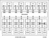
 NVIDIA explained to Anandtech that there was a communication-gap between the engineers (the people who designed the GTX 970 ASIC), and the technical marketing team (the people who write the Reviewer's Guide document, and draw the block-diagram). This team was unaware that with "Maxwell," you could segment components previously thought indivisible, or that you could "partial disable" components.
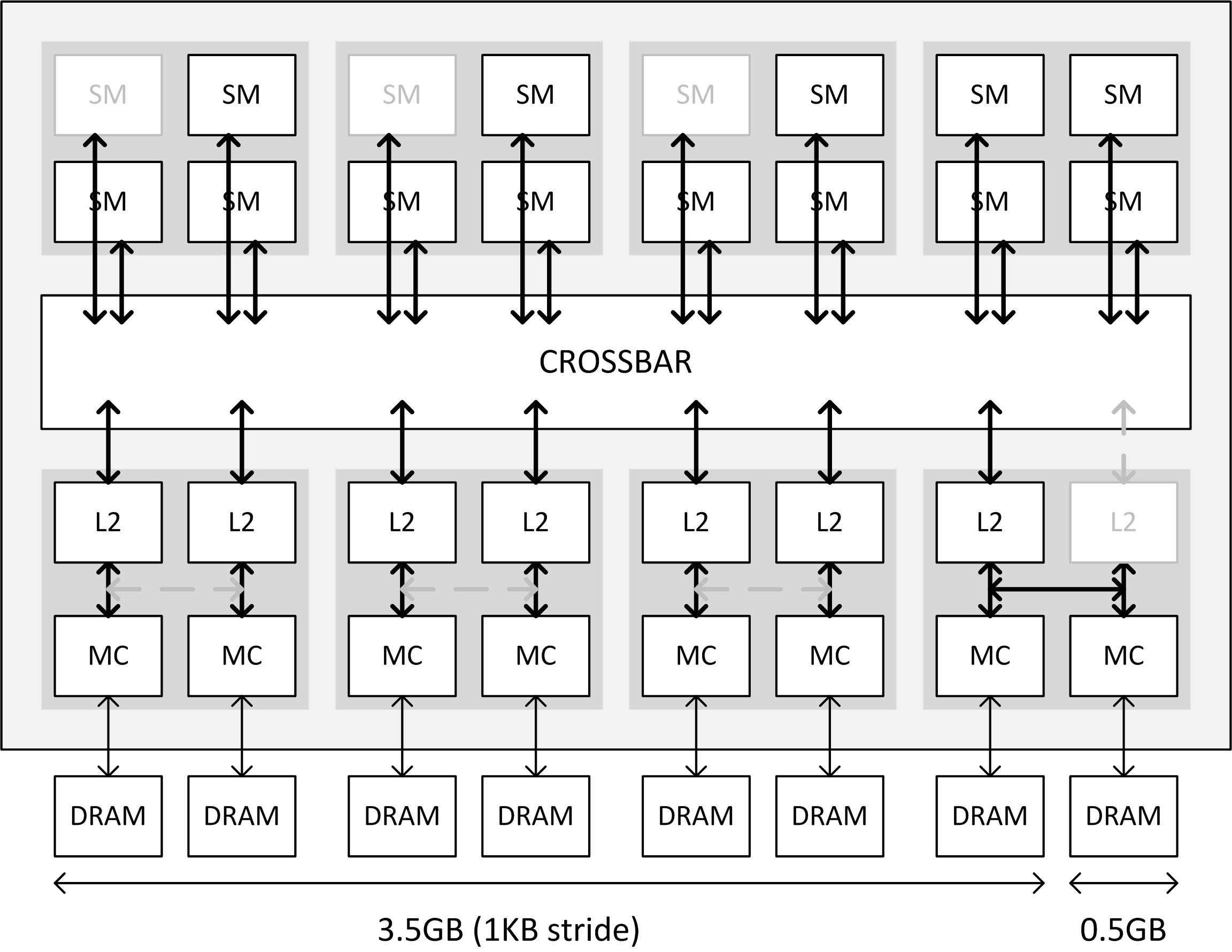
It turns out that in addition to three SMX units being disabled (resulting in 1,664 CUDA cores), NVIDIA reduced the L2 cache (last-level cache) on this chip to 1.75 MB, down from 2 MB, and also disabled a few ROPs. The ROP count is effectively 56, and not 64. The last 8 ROPs aren't "disabled." They're active, but not used, because their connection to the crossbar is too slow (we'll get to that in a bit). The L2 cache is a key component of the "crossbar." Think of the crossbar as a town-square for the GPU, where the various components of the GPU talk to each other by leaving and picking-up data labeled with "from" and "to" addresses. The crossbar routes data between the four Graphics Processing Clusters (GPCs), and the eight memory controllers of 64-bit bus width each (which together make up its 256-bit wide memory interface), and is cushioned by the L2 cache.
The L2 cache itself is segmented, and isn't a monolithic slab of SRAM. Each of the eight memory controllers on the GM204 is ideally tied to its segment of the L2 cache. Also tied to these segments are segments of ROPs. With NVIDIA reducing the L2 cache amount by disabling one such segment. Its component memory controller is instead rerouted to the cache segment of a neighbouring memory controller. Access to the crossbar for that memory controller is hence slower. To make sure there are no issues caused to the interleaving of these memory controllers, adding up to the big memory amount figure that the driver can address, NVIDIA partitioned the 4 GB of memory to two segments. The first is 3.5 GB large, and is made up of memory controllers with access to their own segments of the L2; the second segment is 512 MB in size, and is tied to that memory controller which is rerouted.
The way this partitioning works, is that the 3.5 GB partition can't be read while the 512 MB one is being read. Only to an app that's actively using the entire 4 GB of memory, there will be a drop in performance, because the two segments aren't being read at the same time. The GPU is either addressing the 3.5 GB segment, or the 512 MB one. Hence, there's a drop in performance to be expected, again, for apps that use up the entire 4 GB of memory.
While it's technically correct that the GTX 970 has a 256-bit wide memory interface, and given its 7.00 GHz (GDDR5-effective) memory clock, that translates to 224 GB/s of bandwidth on paper, not all of that memory is uniformly fast. You have 3.5 GB of it having normal access to the crossbar (the town-square of the GPU), and 512 MB of it having slower access. Therefore, the 3.5 GB segment really just has 196 GB/s of memory bandwidth (7.00 GHz x 7 ways to reach the crossbar x 32-bit width per chip), which can be said with certainty. Nor can we say how this segment affects the performance of the memory controller whose crossbar port it's using, if the card is using its full 4 GB. We can't tell how fast the 512 MB second segment really is. But it's impossible for the second segment to make up 28 GB/s (of the 224 GB/s), since NVIDIA itself claims this segment is running slower. Therefore NVIDIA's claims of GTX 970 memory bandwidth being 224 GB/s at reference clocks is inaccurate.
Why NVIDIA chose to reduce cache size and ROP count will remain a mystery. We can't imagine that the people designing the chip will not have sufficiently communicated this to the driver and technical marketing teams. To claim that technical marketing didn't get this the first time around, seems like a hard-sell. We're pretty sure that NVIDIA engineers read reviews, and if they saw "64 ROPs" on a first-page table, they would have reported it up the food-chain at NVIDIA. An explanation about this hardware change should have taken up an entire page in the technical documents the first time around, and NVIDIA could have saved itself a lot of explanation, much of it through the press.
Source:
Anandtech
According to an Anandtech report, which cites that easy explanation from NVIDIA, the company was not truthful about specs of GTX 970, at launch. For example, the non-public document NVIDIA gave out to reviewers (which gives them detailed tech-specs), had clearly mentioned ROP count of the GTX 970 to be 64. Reviewers used that count in their reviews. TechPowerUp GPU-Z shows ROP count as reported by the driver, but it has no way of telling just how many of those "enabled" ROPs are "active." The media reviewing the card were hence led to believe that the GTX 970 was carved out by simply disabling three out of sixteen streaming multiprocessors (SMMs), the basic indivisible subunits of the GM204 chip, with no mention of other components like the ROP count, and L2 cache amount being changed from the GTX 980 (a full-fledged implementation of this silicon).

It turns out that in addition to three SMX units being disabled (resulting in 1,664 CUDA cores), NVIDIA reduced the L2 cache (last-level cache) on this chip to 1.75 MB, down from 2 MB, and also disabled a few ROPs. The ROP count is effectively 56, and not 64. The last 8 ROPs aren't "disabled." They're active, but not used, because their connection to the crossbar is too slow (we'll get to that in a bit). The L2 cache is a key component of the "crossbar." Think of the crossbar as a town-square for the GPU, where the various components of the GPU talk to each other by leaving and picking-up data labeled with "from" and "to" addresses. The crossbar routes data between the four Graphics Processing Clusters (GPCs), and the eight memory controllers of 64-bit bus width each (which together make up its 256-bit wide memory interface), and is cushioned by the L2 cache.
The L2 cache itself is segmented, and isn't a monolithic slab of SRAM. Each of the eight memory controllers on the GM204 is ideally tied to its segment of the L2 cache. Also tied to these segments are segments of ROPs. With NVIDIA reducing the L2 cache amount by disabling one such segment. Its component memory controller is instead rerouted to the cache segment of a neighbouring memory controller. Access to the crossbar for that memory controller is hence slower. To make sure there are no issues caused to the interleaving of these memory controllers, adding up to the big memory amount figure that the driver can address, NVIDIA partitioned the 4 GB of memory to two segments. The first is 3.5 GB large, and is made up of memory controllers with access to their own segments of the L2; the second segment is 512 MB in size, and is tied to that memory controller which is rerouted.
The way this partitioning works, is that the 3.5 GB partition can't be read while the 512 MB one is being read. Only to an app that's actively using the entire 4 GB of memory, there will be a drop in performance, because the two segments aren't being read at the same time. The GPU is either addressing the 3.5 GB segment, or the 512 MB one. Hence, there's a drop in performance to be expected, again, for apps that use up the entire 4 GB of memory.
While it's technically correct that the GTX 970 has a 256-bit wide memory interface, and given its 7.00 GHz (GDDR5-effective) memory clock, that translates to 224 GB/s of bandwidth on paper, not all of that memory is uniformly fast. You have 3.5 GB of it having normal access to the crossbar (the town-square of the GPU), and 512 MB of it having slower access. Therefore, the 3.5 GB segment really just has 196 GB/s of memory bandwidth (7.00 GHz x 7 ways to reach the crossbar x 32-bit width per chip), which can be said with certainty. Nor can we say how this segment affects the performance of the memory controller whose crossbar port it's using, if the card is using its full 4 GB. We can't tell how fast the 512 MB second segment really is. But it's impossible for the second segment to make up 28 GB/s (of the 224 GB/s), since NVIDIA itself claims this segment is running slower. Therefore NVIDIA's claims of GTX 970 memory bandwidth being 224 GB/s at reference clocks is inaccurate.
Why NVIDIA chose to reduce cache size and ROP count will remain a mystery. We can't imagine that the people designing the chip will not have sufficiently communicated this to the driver and technical marketing teams. To claim that technical marketing didn't get this the first time around, seems like a hard-sell. We're pretty sure that NVIDIA engineers read reviews, and if they saw "64 ROPs" on a first-page table, they would have reported it up the food-chain at NVIDIA. An explanation about this hardware change should have taken up an entire page in the technical documents the first time around, and NVIDIA could have saved itself a lot of explanation, much of it through the press.
138 Comments on GTX 970 Memory Drama: Plot Thickens, NVIDIA has to Revise Specs
But NVidia has basically lied about hardware specifications. I don't believe for a second this was all one big mistake of somebody not saying to marketing that the card did not in fact have 64 ROPs and 224GB/s bandwidth. By all accounts it's pretty crappy business practice, and they should be punished accordingly.
That being said. I still like my 3.5GB 970 for the price I got it at.
The truth is once the card gets a to a rez where 4gb would even be worth having the GPU cant handle it and it would make maybe 1-2fps difference at best, its been show time and time again, 256bit bus really can only handle 2gb.
If this customer backlash gains traction it could result is a class action lawsuit. I'm certain with a market cap of 11 billion it would attract a top gun law firm to handle it.
It ain't a question about speed, but common sense. nVidia played faul.
For example AMD got TLB bug on K10, they force fixed it via kernel patch to all, despite it caused BSOD in very few specialized tasks, but yet they played clean.
Intel also plays clean and errata documents are available on Intel site and describes what stepping did correct for each CPU, thus kernels are patched and aware and disable many features, mostly virtualization sub features those are often broken. As all consumer semiconductor makers do with their device data sheet, it's been since 1950ties.
This time it is more than fishy. They actually intended to make such obscure design, they could save more on that one single memory chip, as it really give 2-5% max performance delta as they say. Doing that just for marketing and for the sake of round 4GB number?(noob user actually thinks it is the main criteria, OK yes) And spoofing the ROP count, just why(noob user doesn't know what it is). Gosh this is low... I am actually disappointed having nvidia cards in the past then a bit.
Although... everyone remembers the FX series bloop with broken DX9c shaders, they also acted a bit the same, there was a recall for them?
Well I guess it will bring up more AMD users, as they need dough really bad in order to keep them alive and maintain the competition. As the green camp is getting funny ideas and their marketing team smoking way too green stuff.
Ironically, I downgraded from a pair of Titans to a pair of 980s(side grade? iono). For a simple reason, Shadowplay works at 4k@60FPS. It does not with AMD, and it is not possible using fraps, dxtory, or the like(see my vraps, 4x256gb SSD raid 0(lsi 9266-4i). I can record, and upload 4k video's now that look good.
While I doubt many people here or anywhere were concerned with the ROP count, the L2 Cache, among other things it is still not right to lie to your customers. Performance has not changed and the numbers seen before still stand, however the 3.5gb is the most concerning part to those running the extreme areas of gaming and still could have effected a small amount of users decisions (I am being conservative with that). Even if just 5% would have changed their minds based on this information that is 5% of the people who purchased the card that feel ripped off in some way (Random number, not an actual figure). I don't find the way they are handling this to be smart nor the way it started out to begin with smart.
What is very hard to believe is that after months passed, and hundreds of reviews and articles, nobody at nVidia noticed the errors on so many reviews up until now. (Which if it was the case, it would prove they just don't give a damn what the reviews say, as long as they give a nice final grade and Pro/Cons appraisal.)
That said, it might mean that they did noticed the info/marketing "mistake" but didn't say anything until now because the card was working as intended anyway, getting mega hype, getting big sales, and pointing out the info mistake would actually be a possible marketing "downgrade", since the card was doing so well and AMD has no new response until Q2. So they just kept quiet, since this was detected only under specific games+settings, reviewers didn't even catch the info issue, and they just decided to shrug their shoulders... hoping that those user reports being made were just something considered by others as inaccurate or just non-relevant to the point of making a fuss about it. A gamble that failed completely.
I'd have bought the cards for the potential 4GB memory. If my experience could have been marred by this, in scenario's where 4k used over 3.5GB, I would be angry.
But, I read reviews and sli 970's seemed weaker than other options. I stayed with my 780ti and sli'd that instead.
This very poor PR for NV. Kind of impossible to defend the lie. Great card but needs to be formally rebranded as 3.5GB.
False advertising aside, they had to neuter it. Next time though a little heads up will save them a lot of PR crap.
Edit: After checking the article from yesterday, the table included that showed the effects of running <3.5GB and >3.5GB were almost identical in the performance hit on both the 980 and the 970. If that is true, then someone is still lying.
idk, it seemed the TR, PCper and esp. anand tech articles made it quite clear. though i do seem to have a talent at solving murder mysteries within the first chapter of the book.
" We can't imagine that the people designing the chip will not have sufficiently communicated this to the driver and technical marketing teams."
do you think they go out and have after work drinks? i'd be surprise if they're in the same building let alone on the same floor. in a perfect world all departments communicate well w/each other. however in the real world it is lacking.
"To claim that technical marketing didn't get this the first time around, seems like a hard-sell. We're pretty sure that NVIDIA engineers read reviews, and if they saw "64 ROPs" on a first-page table, they would have reported it up the food-chain at NVIDIA."
word on the street is the engineers were too busy watching kitty cat videos while eating cheetos.
"An explanation about this hardware change should have taken up an entire page in the technical documents the first time around, and NVIDIA could have saved itself a lot of explanation, much of it through the press."
yeah and i am surprised that technology journalists who have reported for years didn't see the asymmetrical design also. hopefully they will learn from nvidia's mistake as well.
edit: oh yeah HI, i am new :)
I mean if nobody found out about this "anomaly", NVIDIA will not say anything. Thats for sure. I mean its been months since 970 was out and they only found out now?
And response was a communication gap between each NVIDIA departments? For sure they lock this parts in purpose. so when they unlocked it, they will call it 970ti. Look at 780 and 780ti. 780 ti was just unlocked 780. am i right?
In theory, they could merge the memory pool and share it through PCIe, but I think OS doesn't really support that and GPU's aren't on the level where shaders could co-operate between GPU's in a seamless way in a way where you could just easily stack things up together.