Tuesday, January 27th 2015

GTX 970 Memory Drama: Plot Thickens, NVIDIA has to Revise Specs
It looks like NVIDIA's first response to the GeForce GTX 970 memory allocation controversy clearly came from engineers who were pulled out of their weekend plans, and hence was too ambiguously technical (even for us). It's only on Monday that NVIDIA PR swung into action, offering a more user-friendly explanation on what the GTX 970 issue is, and how exactly did they carve the GM204 up, when creating the card.
According to an Anandtech report, which cites that easy explanation from NVIDIA, the company was not truthful about specs of GTX 970, at launch. For example, the non-public document NVIDIA gave out to reviewers (which gives them detailed tech-specs), had clearly mentioned ROP count of the GTX 970 to be 64. Reviewers used that count in their reviews. TechPowerUp GPU-Z shows ROP count as reported by the driver, but it has no way of telling just how many of those "enabled" ROPs are "active." The media reviewing the card were hence led to believe that the GTX 970 was carved out by simply disabling three out of sixteen streaming multiprocessors (SMMs), the basic indivisible subunits of the GM204 chip, with no mention of other components like the ROP count, and L2 cache amount being changed from the GTX 980 (a full-fledged implementation of this silicon).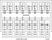
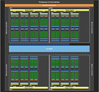 NVIDIA explained to Anandtech that there was a communication-gap between the engineers (the people who designed the GTX 970 ASIC), and the technical marketing team (the people who write the Reviewer's Guide document, and draw the block-diagram). This team was unaware that with "Maxwell," you could segment components previously thought indivisible, or that you could "partial disable" components.
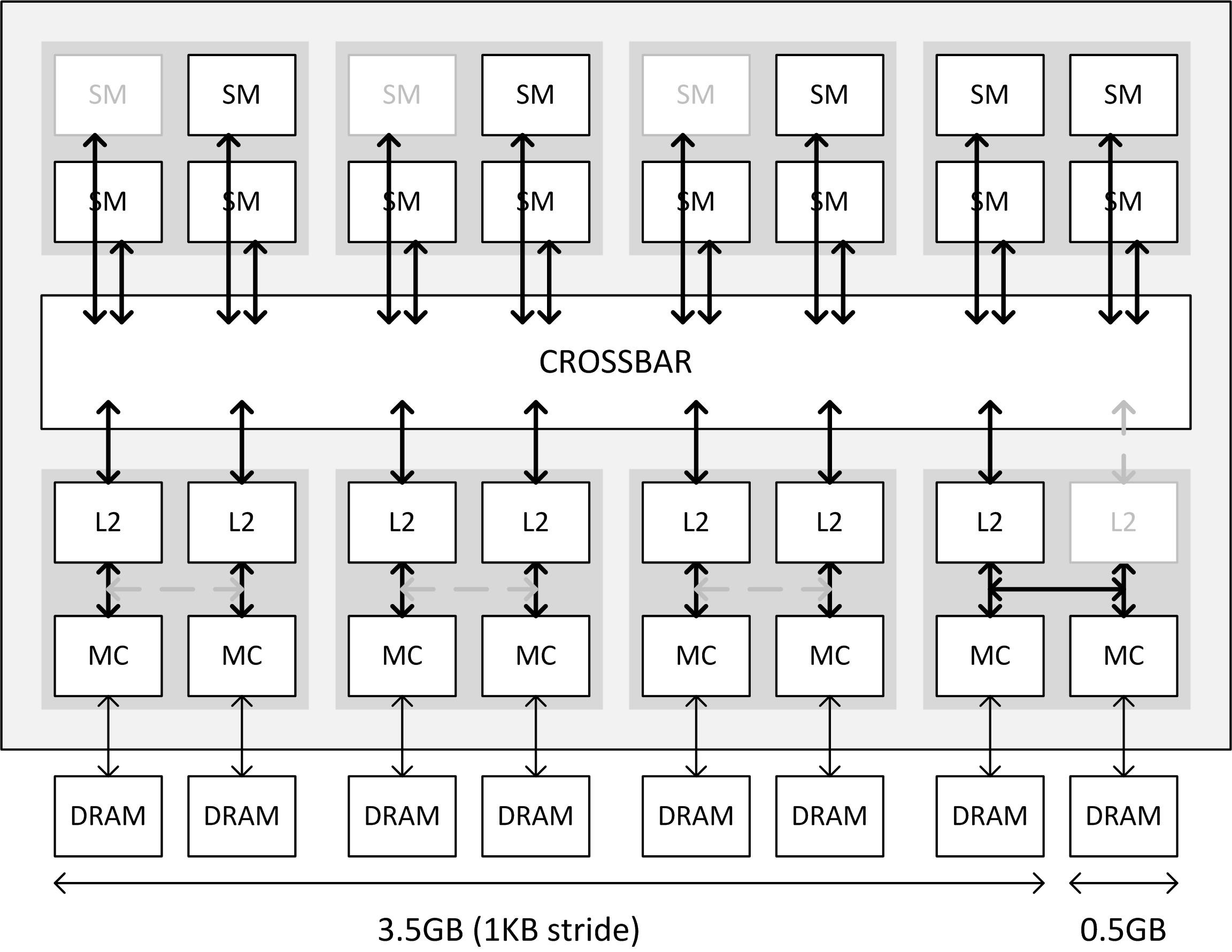
It turns out that in addition to three SMX units being disabled (resulting in 1,664 CUDA cores), NVIDIA reduced the L2 cache (last-level cache) on this chip to 1.75 MB, down from 2 MB, and also disabled a few ROPs. The ROP count is effectively 56, and not 64. The last 8 ROPs aren't "disabled." They're active, but not used, because their connection to the crossbar is too slow (we'll get to that in a bit). The L2 cache is a key component of the "crossbar." Think of the crossbar as a town-square for the GPU, where the various components of the GPU talk to each other by leaving and picking-up data labeled with "from" and "to" addresses. The crossbar routes data between the four Graphics Processing Clusters (GPCs), and the eight memory controllers of 64-bit bus width each (which together make up its 256-bit wide memory interface), and is cushioned by the L2 cache.
The L2 cache itself is segmented, and isn't a monolithic slab of SRAM. Each of the eight memory controllers on the GM204 is ideally tied to its segment of the L2 cache. Also tied to these segments are segments of ROPs. With NVIDIA reducing the L2 cache amount by disabling one such segment. Its component memory controller is instead rerouted to the cache segment of a neighbouring memory controller. Access to the crossbar for that memory controller is hence slower. To make sure there are no issues caused to the interleaving of these memory controllers, adding up to the big memory amount figure that the driver can address, NVIDIA partitioned the 4 GB of memory to two segments. The first is 3.5 GB large, and is made up of memory controllers with access to their own segments of the L2; the second segment is 512 MB in size, and is tied to that memory controller which is rerouted.
The way this partitioning works, is that the 3.5 GB partition can't be read while the 512 MB one is being read. Only to an app that's actively using the entire 4 GB of memory, there will be a drop in performance, because the two segments aren't being read at the same time. The GPU is either addressing the 3.5 GB segment, or the 512 MB one. Hence, there's a drop in performance to be expected, again, for apps that use up the entire 4 GB of memory.
While it's technically correct that the GTX 970 has a 256-bit wide memory interface, and given its 7.00 GHz (GDDR5-effective) memory clock, that translates to 224 GB/s of bandwidth on paper, not all of that memory is uniformly fast. You have 3.5 GB of it having normal access to the crossbar (the town-square of the GPU), and 512 MB of it having slower access. Therefore, the 3.5 GB segment really just has 196 GB/s of memory bandwidth (7.00 GHz x 7 ways to reach the crossbar x 32-bit width per chip), which can be said with certainty. Nor can we say how this segment affects the performance of the memory controller whose crossbar port it's using, if the card is using its full 4 GB. We can't tell how fast the 512 MB second segment really is. But it's impossible for the second segment to make up 28 GB/s (of the 224 GB/s), since NVIDIA itself claims this segment is running slower. Therefore NVIDIA's claims of GTX 970 memory bandwidth being 224 GB/s at reference clocks is inaccurate.
Why NVIDIA chose to reduce cache size and ROP count will remain a mystery. We can't imagine that the people designing the chip will not have sufficiently communicated this to the driver and technical marketing teams. To claim that technical marketing didn't get this the first time around, seems like a hard-sell. We're pretty sure that NVIDIA engineers read reviews, and if they saw "64 ROPs" on a first-page table, they would have reported it up the food-chain at NVIDIA. An explanation about this hardware change should have taken up an entire page in the technical documents the first time around, and NVIDIA could have saved itself a lot of explanation, much of it through the press.
Source:
Anandtech
According to an Anandtech report, which cites that easy explanation from NVIDIA, the company was not truthful about specs of GTX 970, at launch. For example, the non-public document NVIDIA gave out to reviewers (which gives them detailed tech-specs), had clearly mentioned ROP count of the GTX 970 to be 64. Reviewers used that count in their reviews. TechPowerUp GPU-Z shows ROP count as reported by the driver, but it has no way of telling just how many of those "enabled" ROPs are "active." The media reviewing the card were hence led to believe that the GTX 970 was carved out by simply disabling three out of sixteen streaming multiprocessors (SMMs), the basic indivisible subunits of the GM204 chip, with no mention of other components like the ROP count, and L2 cache amount being changed from the GTX 980 (a full-fledged implementation of this silicon).

It turns out that in addition to three SMX units being disabled (resulting in 1,664 CUDA cores), NVIDIA reduced the L2 cache (last-level cache) on this chip to 1.75 MB, down from 2 MB, and also disabled a few ROPs. The ROP count is effectively 56, and not 64. The last 8 ROPs aren't "disabled." They're active, but not used, because their connection to the crossbar is too slow (we'll get to that in a bit). The L2 cache is a key component of the "crossbar." Think of the crossbar as a town-square for the GPU, where the various components of the GPU talk to each other by leaving and picking-up data labeled with "from" and "to" addresses. The crossbar routes data between the four Graphics Processing Clusters (GPCs), and the eight memory controllers of 64-bit bus width each (which together make up its 256-bit wide memory interface), and is cushioned by the L2 cache.
The L2 cache itself is segmented, and isn't a monolithic slab of SRAM. Each of the eight memory controllers on the GM204 is ideally tied to its segment of the L2 cache. Also tied to these segments are segments of ROPs. With NVIDIA reducing the L2 cache amount by disabling one such segment. Its component memory controller is instead rerouted to the cache segment of a neighbouring memory controller. Access to the crossbar for that memory controller is hence slower. To make sure there are no issues caused to the interleaving of these memory controllers, adding up to the big memory amount figure that the driver can address, NVIDIA partitioned the 4 GB of memory to two segments. The first is 3.5 GB large, and is made up of memory controllers with access to their own segments of the L2; the second segment is 512 MB in size, and is tied to that memory controller which is rerouted.
The way this partitioning works, is that the 3.5 GB partition can't be read while the 512 MB one is being read. Only to an app that's actively using the entire 4 GB of memory, there will be a drop in performance, because the two segments aren't being read at the same time. The GPU is either addressing the 3.5 GB segment, or the 512 MB one. Hence, there's a drop in performance to be expected, again, for apps that use up the entire 4 GB of memory.
While it's technically correct that the GTX 970 has a 256-bit wide memory interface, and given its 7.00 GHz (GDDR5-effective) memory clock, that translates to 224 GB/s of bandwidth on paper, not all of that memory is uniformly fast. You have 3.5 GB of it having normal access to the crossbar (the town-square of the GPU), and 512 MB of it having slower access. Therefore, the 3.5 GB segment really just has 196 GB/s of memory bandwidth (7.00 GHz x 7 ways to reach the crossbar x 32-bit width per chip), which can be said with certainty. Nor can we say how this segment affects the performance of the memory controller whose crossbar port it's using, if the card is using its full 4 GB. We can't tell how fast the 512 MB second segment really is. But it's impossible for the second segment to make up 28 GB/s (of the 224 GB/s), since NVIDIA itself claims this segment is running slower. Therefore NVIDIA's claims of GTX 970 memory bandwidth being 224 GB/s at reference clocks is inaccurate.
Why NVIDIA chose to reduce cache size and ROP count will remain a mystery. We can't imagine that the people designing the chip will not have sufficiently communicated this to the driver and technical marketing teams. To claim that technical marketing didn't get this the first time around, seems like a hard-sell. We're pretty sure that NVIDIA engineers read reviews, and if they saw "64 ROPs" on a first-page table, they would have reported it up the food-chain at NVIDIA. An explanation about this hardware change should have taken up an entire page in the technical documents the first time around, and NVIDIA could have saved itself a lot of explanation, much of it through the press.
138 Comments on GTX 970 Memory Drama: Plot Thickens, NVIDIA has to Revise Specs
Having said that, how many mirrors must AMD's hierarchy broken, and how many black cats crossed their paths? Every time the competition slips up - this, Intel's Cougar Point SATA bug, Nvidia's 40nm woes (and the list goes on), and AMD are never in a position to capitalize.
When AMD WAS competitive back in the days of P3 1.13GHz recall & horrendus 1st Gen P4 efficiency, their K7 and K8 based CPU did manage to capitalize on those.
Either way in the end, all this can only make things better for everyone as it just shows people will at least put there foot down (Well at least enough to make a difference). This will help NVidia in the future with their next products not make the same mistakes.
The GTX970 is my first foray to the green team since my 8600GT and it crossed oceans to get from the store to me, so swaps/refunds ain't really an option for me.
Give us free Witcher 3 preorder keys (and some other decent options like Mortal Kombat X / Arkham Knight / Resident Evil for those that want others) and let's call it a day, nVIDIA.
I didn't really pay any attention to computers until I needed a new machine and built one last year. I initially looked at only AMD, because they were good last time I checked (2008), and I like the underdog. You could have called me a fan-boy. But as I got into the details I changed my mind.
I think Nvidia is losing a chunk of money even in the most ideal scenario.
Oh... and AMD is currently losing money while Nvidia and Intel are not. How to fix that? Cut "wasteful" R&D even more?
FTC - Truth In Advertising
Nvidia is based in California
California - Truth In Advertising
Lawyers will decide where the money can be squeezed out from the best.
So what is the excuse when AMD launched the Evergreen series (HD 5000) in September 2009? Between the launching of the HD 5970 (fastest card during virtually its entire lifetime), 5870, 5850 (best bang for buck card of its era), 5770 (best mainstream card of its era), and 5750, and the arrival of Nvidia's Fermi architecture at the end of March 2010, Nvidia fielded nothing newer than an 18-month old GT200 and an almost 2.5 year old G92.....yet AMD's discrete graphics market share actually declined.
It also doesn't explain how AMD's market share is steadily declining while the company still generally being first to market with new graphics architectures (Evergreen launched before Fermi, Southern Islands launched before Kepler).
And K7 and K8? At the height of AMD's competitiveness, the company never accounted for more than 25.3% of the x86 processor market, which was achieved in Q1 2006.
imo the reason AMD struggles so much is they charged too little for their chips. This is evidenced in the Profit Margin for AMD and Nvidia and Intel.
NVIDIA Corporation
Key stats and ratios
Q4 (Oct '14) 2014
Net profit margin 14.12% 10.65%
Operating margin 17.41% 12.01%
EBITD margin - 18.51%
Return on average assets 10.04% 6.44%
Return on average equity 16.31% 9.48%
Employees 8,808 -
CDP Score - 87 B
www.google.com/finance?cid=662925
Advanced Micro Devices, Inc.
Key stats and ratios
Q3 (Sep '14) 2013
Net profit margin 1.19% -1.57%
Operating margin 4.41% 1.92%
EBITD margin - 6.10%
Return on average assets 1.59% -1.99%
Return on average equity 13.16% -15.34%
Employees 10,671 -
CDP Score - 67 C
www.google.com/finance?q=NASDAQ:AMD&ei=hEjJVMCCFOOWsge1goDYCw
Intel Corporation
Key stats and ratios
Q3 (Sep '14) 2013
Net profit margin 22.79% 18.25%
Operating margin 30.97% 23.09%
EBITD margin - 39.01%
Return on average assets 14.59% 10.89%
Return on average equity 23.07% 17.58%
Employees 105,600 -
CDP Score - 85 B
www.google.com/finance?q=NASDAQ:INTC&ei=yEnJVNn3FJOTsgfRnYHYCg
Well, regarding AMD's market share in x86, their historical 25.3% figure was achieved because of the major success of K7 and K8. Don't forget Q1 2006 was about 6 months before Intel managed to return to dominance with their Core 2 series of CPUs. During the period between P3 Coppermine and Conroe, most enthusiasts and IT literate gamers had Athlon XP, 64, 64 X2, FX or Opeteron in their PCs. And I almost forgot that NV also got a free ride with their nForce chipsets on AMD's success at the time.
The reason of AMD's market share mediocrity is actually fairly simple. The company was founded on a sales/marketing foundation, Intel and Nvidia (and ATI for that matter) were founded on engineering. When you have substantial saleable IP from the get-go and it arrives at market in good shape, the company has a decided advantage (AMD's early years are mostly about making licensed copies of Fairchild TTL chips, Intel ROM/EPROM/SRAM/processors, analog circuits) in mindshare - firstly from the engineers in the companies they deal with, and later the roll-on effect to end users with the establishment of the brand. Once the brand has been established, any rival has to not only deliver better product, but the incumbent market leader also has to fail. Aside from the occasional blip, these two things have never occurred simultaneously to give AMD any advantage. Without the brand and IP basis, the company is playing follow-the-leader, it can't charge as much for products, it's margins are lower (see 64K's post above as example), and with lower revenue it can't take the financial risks on expansion and R&D without a greater risk of compromising the integrity of the company - you then sit at the crux of a damned if you do, damned if you don't situation. Play it safe (Cyrix, Mostek, S3, Matrox, Chips & Technologies etc.) and undergo death by a thousand cuts, or buy IP as a shortcut but incurring debt - as AMD did with the purchases of ATI, NexGen, the DEC licenses etc.
It also doesn't help that AMD promote the "underdog" persona - plenty of people root for the underdog, but a much larger percentage of people want to allied with the dominant brand.
2006 was the year that Nvidia jumped way ahead of ATI/AMD, and they've held about a 60% vs 40% market share lead in discrete graphics since then. Recently though, Nvidia's share has jumped to 72%. 40% to 28% in half a year is a steep decline for AMD. You could say that is a temporary thing and AMD will come on strong after they introduce new cards this year... but that remains to be seen. I fully expect AMD's top card to beat the GTX 980 in performance, but it will be 28nm and likely no more power efficient than previous AMD offerings, which means it will be a beast. Lower down the pecking order I don't expect their new cards to be any more impressive than the R9 285.