Wednesday, November 18th 2015

NVIDIA Details "Pascal" Some More at GTC Japan

NVIDIA revealed more details of its upcoming "Pascal" GPU architecture at the Japanese edition of the Graphics Technology Conference. The architecture will be designed to nearly double performance/Watt over the current "Maxwell" architecture, by implementing the latest tech. This begins with stacked HBM2 (high-bandwidth memory 2). The top "Pascal" based product will feature four 4-gigabyte HBM2 stacks, totaling 16 GB of memory. The combined memory bandwidth for the chip will be 1 TB/s. Internally, bandwidths can touch as high as 2 TB/s. The chip itself will support up to 32 GB of memory, and so enterprise variants (Quadro, Tesla), could max out the capacity. The consumer GeForce variant is expected to serve up 16 GB.

It's also becoming clear that NVIDIA will build its "Pascal" chips on the 16 nanometer FinFET process (AMD will build its next-gen chips on more advanced 14 nm process). NVIDIA is innovating a new interconnect called NVLink, which will change the way the company has been building dual-GPU graphics cards. Currently, dual-GPU cards are essentially two graphics cards on a common PCB, with PCIe bandwidth from the slot shared by a bridge-chip, and an internal SLI bridge connecting the two GPUs. With NVLink, the two GPUs will be interconnected with an 80 GB/s bi-directional data path, letting each GPU directly address memory controlled by the other. This should greatly improve memory management in games that take advantage of newer APIs such as DirectX 12 and Vulkan; and prime the graphics card for higher display resolutions. NVIDIA is expected to launch its first "Pascal" based products in the first half of 2016.
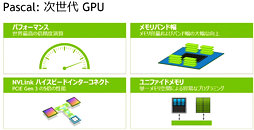
Source: VR World
Add your own comment

67 Comments on NVIDIA Details "Pascal" Some More at GTC Japan

#26
Estaric
Easo1TB/sec?
Well, damn...
i thought they same thing!
Posted on Reply
#28
Fluffmeister
Hitman_ActualHell yah! bring it! Excited for Pascal!
Ditto my friend, ditto! :O
Posted on Reply
#29
FreedomEclipse
~Technological Technocrat~
荷兰大母猪次世代GPU?3倍-5倍性能?本当?
In English please?
Posted on Reply
#31
HM_Actua1
LET THE MILLENNIALS AND AMD FB RAGE BEGIN!

Pascal will smoke everything out there
Posted on Reply
#32
dorsetknob
"YOUR RMA REQUEST IS CON-REFUSED"
荷兰大母猪次世代GPU?3倍-5倍性能?本当?
FreedomEclipseIn English please?
rough translation
Next-Gen GPU? 3 times-5 times times performance? The simple necessities?

:) "" 3 times-5 times times performance? "" Dream on
Posted on Reply
#33
cadaveca
My name is Dave
qubitI'm really looking forward to that unified memory architecture and the elimination of SLI problems.
Unified memory will not alone fix SLI problems. Most issues are more about proper resource management than it is about not having shared memory, although post-processing will be a bit easier to manage if NV-Link does what it is purported to be able to do. The big boon of shared memory is the added addressing space as well as the ability to store more data allowing for greater detail.
Posted on Reply
#34
qubit
Overclocked quantum bit
cadavecaUnified memory will not alone fix SLI problems. Most issues are more about proper resource management than it is about not having shared memory, although post-processing will be a bit easier to manage if NV-Link does what it is purported to be able to do. The big boon of shared memory is the added addressing space as well as the ability to store more data allowing for greater detail.
You might be right, I honestly dunno. I just remember that when this new form of SLI was announced several months ago by NVIDIA (they had a blog post that was reported widely by the tech press, including TPU) it sounded like all these problems would go away. Regardless, I'll bet it will be a big improvement over what we've got now.
Posted on Reply
#35
Solidstate89
AsRockMS says win 10 will allow mixed cards then nVidia come out with this, makes me wounder if they going nuke it and disable the crap out of it all over again.
NVLink has nothing to do with the consumer space and I don't know why people keep assuming it does. It literally replaces the PCI-e standard and adds cost and complexity the system builders neither want nor need. Not to mention the CPU/PCH has to support the capability in order to communicate between the GPU and the CPU.

On top of it, the DX12 explicit multi-GPU mode has to be specifically coded for and enabled by game developers, the GPU vendors have very little to do in implementing it and the drivers have very little if nothing to do with optimizing it due to the low level nature of DX12.

The only option nVidia could possibly have at even approaching NVLink usage in the consumer space is in Dual-GPU cards with two GPU dies on a single PCB, using the NVLink as an interconnect devoted specifically to GPU-to-GPU communications.
Posted on Reply
#36
HumanSmoke
Solidstate89NVLink has nothing to do with the consumer space and I don't know why people keep assuming it does. It literally replaces the PCI-e standard and adds cost and complexity the system builders neither want nor need. Not to mention the CPU/PCH has to support the capability in order to communicate between the GPU and the CPU.
That's about it. Just as Intel is pushing for PCI-E 4.0 and buying Cray's Aries/Gemini interconnect for pushing bandwidth in the big iron war with IBM, the latter has paired with Nvidia (NVLink) and Mellanox to do the exact same thing for OpenPOWER. The fixation some people have with everything tech HAVING to revolve around gaming is perplexing to say the least.
Solidstate89The only option nVidia could possibly have at even approaching NVLink usage in the consumer space is in Dual-GPU cards with two GPU dies on a single PCB, using the NVLink as an interconnect devoted specifically to GPU-to-GPU communications.
That was my understanding also. The only way for Nvidia to get NVLink into the consumer space would be for it to be folded into the PCI-E 4.0 specification, or as an optional dedicated chip in the same way that Avago's PEX lane extender chips are currently used (and Nvidia's own old NF200 predecessor for that matter).
Posted on Reply
#37
cadaveca
My name is Dave
HumanSmokeThat was my understanding also. The only way for Nvidia to get NVLink into the consumer space would be for it to be folded into the PCI-E 4.0 specification, or as an optional dedicated chip in the same way that Avago's PEX lane extender chips are currently used (and Nvidia's own old NF200 predecessor for that matter).
NVLink should allow for direct access to system ram, and that function is already supported by PCIe spec, AFAIK. It's really no different than AMD's "sidebar" that was present on past GPU designs. IBM has already partnered with NVidia for NVLink, so I'm sure we'll see NVidia GPUs paired with PowerPC CPUs in short order.
Posted on Reply
#38
HumanSmoke
cadavecaNVLink should allow for direct access to system ram, and that function is already supported by PCIe spec
The function is, but the bandwidth isn't.
PCI-E bandwidth isn't an issue for consumer GPU in 99%+ situations - as W1zz's many PCIE 1.1/2.0/3.0 comparisons have shown. HPC bandwidth, both intra- and inter-nodal on the other hand....it isn't hard to see how a couple of CPUs feeding eight dual-GPU K80's or next-gen GPUsat 100% workload might produce some different effects regards bandwidth saturation compared to a gaming system.
cadavecaIBM has already partnered with NVidia for NVLink, so I'm sure we'll see NVidia GPUs paired with PowerPC CPUs in short order.
Next year for early access and test/qualification/validation. POWER9 (14nm) won't be ready for prime time until 2017, so the early systems will be based on the current POWER8
Posted on Reply
#39
medi01
Fury is roughly on par with Maxwell on power efficiency.
Interesting, who will have better process, GloFo 14nm or ITMS 16nm.
Samsung's 14nm were rumored to suck.
deemonso much yadaydadayada
Try harder:

1) GSync is as locked down as it gets (to "nope, won't license it to anyone" point)
2) adaptive sync is THE ONLY standard, (DISPLAYPORT 1.2A, THAT IS) there is no "freesync" standard.
3) nothing stops any manufacturer out there to use adaptive sync (dp 1.2a), no need to involve AMD or any of its "freesync" stuff in there
Posted on Reply
#40
cadaveca
My name is Dave
HumanSmokeit isn't hard to see how a couple of CPUs feeding eight dual-GPU K80's or next-gen GPUsat 100% workload might produce some different effects regards bandwidth saturation compared to a gaming system.
I've literally complained about a lack of bandwidth for multi-GPU processing for a long time, only to get things like "mining doesn't need bandwidth!" as responses. GPGPU has been limited by PCIe for the past 5-7 years from my perspective.
Posted on Reply
#41
Darksword
TheGuruStudAnother $1k card, folks. Hell, with that much ram, maybe more.
$1,000.00? HA! This is Nvidia we're talking about.

Try, $2,000.00 at least.
Posted on Reply
#42
matar
I have been waiting for this can't wait, my next build intel broadwell-E with X99 USB 3.1 and nVidia Pascal in SLi
I have skipped 6 and 7 and 9 and 28nm on the Maxwell didn't sell me , is good now its worth the upgrade. next November 2016 black Friday is my new shopping saving from now...
Posted on Reply
#43
FreedomEclipse
~Technological Technocrat~
matarI have been waiting for this can't wait, my next build intel broadwell-E with X99 USB 3.1 and nVidia Pascal in SLi
I have skipped 6 and 7 and 9 and 28nm on the Maxwell didn't sell me , is good now its worth the upgrade. next November 2016 black Friday is my new shopping saving from now...
So a $4000 computer then? Are you going to be F@lding or Crunching to the moon and back?
Posted on Reply
#44
matar
FreedomEclipseSo a $4000 computer then? Are you going to be F@lding or Crunching to the moon and back?
broadwell-E and nVidia Pascal will be available in mid 2016 its not like they are out today and I am buying them next year
Posted on Reply
#45
HumanSmoke
cadavecaI've literally complained about a lack of bandwidth for multi-GPU processing for a long time, only to get things like "mining doesn't need bandwidth!" as responses. GPGPU has been limited by PCIe for the past 5-7 years from my perspective.
Sounds like the responses you've been getting aren't particularly well informed. I did note 99%+ of usage scenarios (current), but there are few people running 3 and 4 card setups, where the performance difference is more obvious...

...for HPC, I think latency is just as much an issue. Just as PCI-E 1.1/2.0 generally manifests as increased frame variance/stutter in comparison to 3.0 in bandwidth limiting scenarios, time to completion for GPGPU workloads is also affected by latency issues. Where time is literally money when selling time on a cluster its easy to see why Nvidia push the reduced latency of NVLink.
Posted on Reply
#46
lilhasselhoffer
Let's rip out the crap that AMD already said, as HBM is their baby. That means the VRAM quantities aren't news.

What we're left with is NVLink. It's interesting, if somewhat disturbing.

Right now single card dual GPU cards are don't scale great and cost a ton of money. NVLink addresses...maybe the first issue. The biggest issue is that even if it solves scaling, you've still got factor 2. As this conclusion is self evident, we're back to the NVLink announcement not being about consumer GPUs. The VRAM side definitely wasn't.

Is this good for HPC, absolutely. Once you stop caring about price, the better the interconnect speed the more you can compute. I applaud Nvidia announcing this for HPC, but it's standing against Intel. Intel is buying up semi-conductor companies for their IP, and working with other companies in their field to corner the HPC market via common interconnects (PCI-e 4.0).

The disturbing part is the upcoming war in which Intel decides to cut PCI-e lanes to make their PCI-e 4.0 standard required. The consumer Intel offerings are already a little sparse on their PCI-e lanes. I don't want Intel deciding to push less PCI-e lanes to penalize Nvidia for NVLink, which will also influence the AMD vs. Nvidia dynamic.


This is interesting, but not news for gamers. Please, show me the Pascal variant with about 8 GB of VRAM that has 60-80% better performance than my current 7970 while sipping power. Until then, thanks but I'm really not the target audience.
Posted on Reply
#47
arbiter
deemonso much misinformation.

Adaptive sync IS FreeSync.

FreeSync is the brand name for an adaptive synchronization technology for LCD displays that support a dynamic refresh rate aimed at reducing screen tearing.[2] FreeSync was initially developed by AMD in response to NVidia's G-Sync. FreeSync is royalty-free, free to use, and has no performance penalty.[3] As of 2015, VESA has adopted FreeSync as an optional component of the DisplayPort 1.2a specification.[4] FreeSync has a dynamic refresh rate range of 9–240 Hz.[3] As of August 2015, Intel also plan to support VESA's adaptive-sync with the next generation of GPU.[5]
Speaking of Misinformation, you quote "wikipedia".
How are DisplayPort Adaptive-Sync and AMD FreeSync™ technology different?
DisplayPort Adaptive-Sync is an ingredient DisplayPort feature that enables real-time adjustment of monitor refresh rates required by technologies like AMD FreeSync™ technology. AMD FreeSync™ technology is a unique AMD hardware/software solution that utilizes DisplayPort Adaptive-Sync protocols to enable user-facing benefits: smooth, tearing-free and low-latency gameplay and video. Users are encouraged to read this interview to learn more.
Source: support.amd.com/en-us/search/faq/214 <---- straight from AMD themselves. In Short words, proprietary use of the protocol
HumanSmokeThe function is, but the bandwidth isn't.
PCI-E bandwidth isn't an issue for consumer GPU in 99%+ situations - as W1zz's many PCIE 1.1/2.0/3.0 comparisons have shown. HPC bandwidth, both intra- and inter-nodal on the other hand....it isn't hard to see how a couple of CPUs feeding eight dual-GPU K80's or next-gen GPUsat 100% workload might produce some different effects regards bandwidth saturation compared to a gaming system.
Well NVlink will allow on a dual gpu card 1 gpu to access the memory of the other card as explained in the brief. Can't really do that with a pipe that so limited that PCI-E is atm. As resolution goes up could likely see benifit of that much higher bandwidth pipe in performance.
Posted on Reply
#48
HumanSmoke
lilhasselhofferThe disturbing part is the upcoming war in which Intel decides to cut PCI-e lanes to make their PCI-e 4.0 standard required. The consumer Intel offerings are already a little sparse on their PCI-e lanes. I don't want Intel deciding to push less PCI-e lanes to penalize Nvidia for NVLink, which will also influence the AMD vs. Nvidia dynamic.
Very unlikely to happen. Intel has been in the past threatened with sanction, and the FTC settlement (aside from being unable to substantially alter PCI-E for another year at least) only makes allowances for Intel's PCI-E electrical lane changes if it benefits their own CPUs - somewhat difficult to envisage as a scenario. Disabling PCI-E would require a justification that would suit both Intel, the FTC, and not incur anti-monopoly suits from add in board vendors (graphics, sound, SSD, RAID, ethernet, wi-fi, expansion options etc.)
The second requirement is that Intel is not allowed to engage in any actions that limit the performance of the PCIe bus on the CPUs and chipsets, which would be a backdoor method of crippling AMD or NVIDIA’s GPUs’ performance. At first glance this would seem to require them to maintain status quo: x16 for GPUs on mainstream processors, and x1 for GPUs on Atom (much to the chagrin of NVIDIA no doubt). However Intel would be free to increase the number of available lanes on Atom if it suits their needs, and there’s also a clause for reducing PCIe performance. If Intel has a valid technological reason for a design change that reduces GPU performance and can prove in a real-world manner that this change benefits the performance of their CPUs, then they can go ahead with the design change. So while Intel is initially ordered to maintain the PCIe bus, they ultimately can make changes that hurt PCIe performance if it improves CPU performance.
Bear in mind that when the FTC made the judgement, PCI-E's relevance was expected to diminish, not be looking at a fourth generation. It's hard to make a case for Intel pulling the plug, or decreasing PCI-E compatibility options when their own server/HPC future is tied to PCI-E 4.0 (and Omni-Path, which has no more relevance to consumer desktops than it's competitor, Mellanox's Infiniband)
lilhasselhofferThis is interesting, but not news for gamers. Please, show me the Pascal variant with about 8 GB of VRAM that has 60-80% better performance than my current 7970 while sipping power. Until then, thanks but I'm really not the target audience.
Performance/Power might be a juggling act depending upon which target market the parts end up for, but Nvidia released numbers for Pascal at SC15. ~ 4 TFLOPs of double precision for the top SKU (presumably GP 100) which probably equates to a 1:3:6 ratio ( FP64:FP32:FP16), so about 12 TFLOPs of single precision.
Posted on Reply
#49
lilhasselhoffer
HumanSmokeVery unlikely to happen. Intel has been in the past threatened with sanction, and the FTC settlement (aside from being unable to substantially alter PCI-E for another year at least) only makes allowances for Intel's PCI-E electrical lane changes if it benefits their own CPUs - somewhat difficult to envisage as a scenario. Disabling PCI-E would require a justification that would suit both Intel, the FTC, and not incur anti-monopoly suits from add in board vendors (graphics, sound, SSD, RAID, ethernet, wi-fi, expansion options etc.)


Bear in mind that when the FTC made the judgement, PCI-E's relevance was expected to diminish, not be looking at a fourth generation. It's hard to make a case for Intel pulling the plug, or decreasing PCI-E compatibility options when their own server/HPC future is tied to PCI-E 4.0 (and Omni-Path, which has no more relevance to consumer desktops than it's competitor, Mellanox's Infiniband)

Performance/Power might be a juggling act depending upon which target market the parts end up for, but Nvidia released numbers for Pascal at SC15. ~ 4 TFLOPs of double precision for the top SKU (presumably GP 100) which probably equates to a 1:3:6 ratio ( FP64:FP32:FP16), so about 12 TFLOPs of single precision.
While I appreciate the fact check, disabling PCI-e wasn't what I was trying to say. What I meant is developing a wholly new interface, and only offering a hand full of PCI-e interconnection. They would effectively make its use possible, but not reasonable. If they can demonstrate the ability to connect any card to their system via PCI-e bus it effectively means they're following the FTC's requirements to the letter of the law (if not the spirit). Nowhere in the FTC's ruling can I find an indication of how many PCI-e lanes are required, only that they must be present and meet PCI-SIG electrical requirements.

For example, instead of introducing PCI-e 4.0, introduce PCE (Platform Connect Experimental). 10 PCE connections are allowed to directly connect to the CPU (not interchangeable with PCI-e), while a single PCI-e lane is connected to the CPU. Intel still provides another 2 PCI-e lanes from the PCH, which don't exactly function as well for a GPU.

Intel decides to go whole hog with PCE, and cut Nvidia out of the HPC market. They allow AMD to cross-license the interconnect (under their sharing agreement for x86), but set up some substantial fees for Nvidia. In effect, Intel provides PCI-e as an option, but those who require interconnect have to forego Nvidia products.


As I read the ruling, this is technically not messing with PCI-e electrically. It's also making the HPC effectively Intel's, because the high performance needs make PCI-e unusable (despite physically being present). It follows along with the theory that PCI-e will be supplanted as well. Have I missed something here?
Posted on Reply
#50
HumanSmoke
lilhasselhofferWhile I appreciate the fact check, disabling PCI-e wasn't what I was trying to say. What I meant is developing a wholly new interface, and only offering a hand full of PCI-e interconnection.
Well, Intel could theoretically turn their back on a specification they basically pushed for, but how does that not affect every vendor not just committed to PCI-E (since 4.0 like previous versions is backwards compatible), but every vendor already preparing PCI-E 4.0 logic ? ( Seems kind of crappy to have vendors showing PCI-E 4.0 logic at an Intel Developers Forum if they planned on shafting them).
lilhasselhofferIf they can demonstrate the ability to connect any card to their system via PCI-e bus it effectively means they're following the FTC's requirements to the letter of the law (if not the spirit).
The FTC's current mandate does not preclude further action (nor that of the EU or DoJ for that matter), as evidenced by the Consent Decree the FTC slapped on it last year.
lilhasselhofferIntel decides to go whole hog with PCE, and cut Nvidia out of the HPC market.
Really?I'm not sure how landing a share of a $325million contract and an ongoing partnership with IBM fits into that. ARM servers/HPCalso use PCI-E, and are also specced for Nvidia GPGPU deployment
lilhasselhofferThey allow AMD to cross-license the interconnect (under their sharing agreement for x86),
Well, that's not going to happen unless AMD bring some IP of similar value to the table. Why would Intel give away IP to a competitor (and I'm talking about HSA here), and why would AMD opt for licensing Intel IP when PCI-E is not only free, it is also used by all other HSA Foundation founder members- Samsung, ARM, Mediatek, Texas Instruments, and of course Qualcomm, whose new server chip business supports PCI-E....and that's without AMD alienating it's own installed discrete graphics user base.

If you don't mind me saying so, that sounds like a completely convoluted and fucked up way to screw over a small IHV. If Intel were that completely mental about putting Nvidia out of business wouldn't they just buy it?
Posted on Reply
Add your own comment
Apr 26th, 2024 19:48 EDT change timezone

New Forum Posts

Popular Reviews

Controversial News Posts