Monday, September 17th 2018

NVIDIA Segregates Turing GPUs; Factory Overclocking Forbidden on the Cheaper Variant

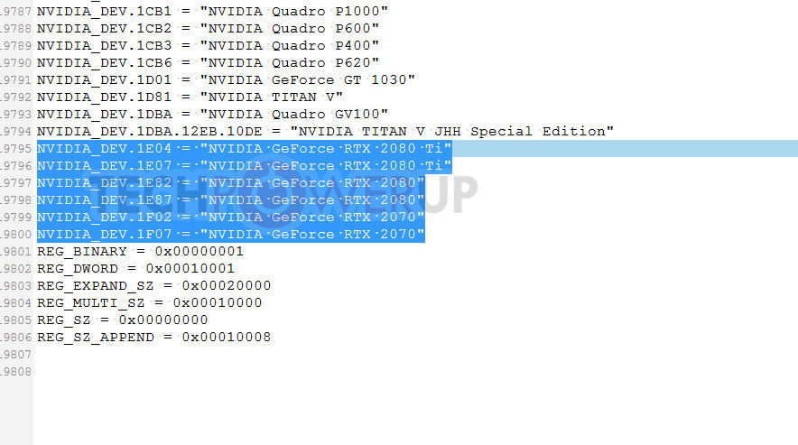
While working on GPU-Z support for NVIDIA's RTX 20-series graphics cards, we noticed something curious. Each GPU model has not one, but two device IDs assigned to it. A device ID is a unique identification that tells Windows which specific device is installed, so it can select and load the relevant driver software. It also tells the driver, which commands to send to the chip, as they vary between generations. Last but not least, the device ID can be used to enable or lock certain features, for example in the professional space. Two device IDs per GPU is very unusual. For example, all GTX 1080 Ti cards, whether reference or custom design, are marked as 1B06. Titan Xp on the other hand, which uses the same physical GPU, is marked as 1B02. NVIDIA has always used just one ID per SKU, no matter if custom-design, reference or Founders Edition.

We reached out to industry sources and confirmed that for Turing, NVIDIA is creating two device IDs per GPU to correspond to two different ASIC codes per GPU model (for example, TU102-300 and TU102-300-A for the RTX 2080 Ti). The Turing -300 variant is designated to be used on cards targeting the MSRP price point, while the 300-A variant is for use on custom-design, overclocked cards. Both are the same physical chip, just separated by binning, and pricing, which means NVIDIA pretests all GPUs and sorts them by properties such as overclocking potential, power efficiency, etc.
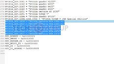
When a board partner uses a -300 Turing GPU variant, factory overclocking is forbidden. Only the more expensive -30-A variants are meant for this scenario. Both can be overclocked manually though, by the user, but it's likely that the overclocking potential on the lower bin won't be as high as on the higher rated chips. Separate device IDs could also prevent consumers from buying the cheapest card, with reference clocks, and flashing it with the BIOS from a faster factory-overclocked variant of that card (think buying an MSI Gaming card and flashing it with the BIOS of Gaming X).

All Founders Edition and custom designs that we could look at so far, use the same -300-A GPU variant, which means the device ID is not used to separate Founders Edition from custom design cards.
Add your own comment

90 Comments on NVIDIA Segregates Turing GPUs; Factory Overclocking Forbidden on the Cheaper Variant

#26
jabbadap
iOSo they found an additional income by charging a premium for binned chips if the AIBs want to offer OC models.
And we customer are no longer able to get a cheap card and OC it for extra performance. Yay!
This is more like a AMD Radeon RX 580 XTR vs XTX, for exemption nvidia prohibit AIBs to factory over clock xtx version of Geforce RTX.
B-RealAnd I bet that will influence the warranty and they will say "you OCd it, no rebate/repair".
Well Tom Petersen said on Gamers Nexus that Nvidia does not even look if gpu is OC at RMA process.
Posted on Reply
#27
R0H1T
This is gonna be interesting :laugh:
Posted on Reply
#28
DeathtoGnomes
It does not say the end user, you the buyer of said card, cant overclock. It infers some binned chips cannot be sold pre-overclocked.

It appears that purpose of dual device IDs is so AIBs can tell the difference. It also might be an attempt to prevent the changing of devices IDs. And/Or also to keep etailers from more price gouging and selling the lesser/weaker binned chips at the same price as OC variants and keep them closer to MRSP pricing.

2cp
Posted on Reply
#29
kings
I don't get all the drama, this was already happening for years, but now, instead of being AIBs making the selection of the best chips for certain versions, it's Nvidia itself.

No chip will be blocked for OC, but cards with better cooling and better power design, will receive the more binned chips to overclock even better. Which make perfect sense, since the buyer of an Zotac AMP! Extreme for example, pay more for that than who buys a basic Zotac card.
Posted on Reply
#30
DeathtoGnomes
kingsNo chip will be blocked for OC, but cards with better cooling and better power design, will receive the more binned chips to overclock even better. Which make perfect sense, since the buyer of an Zotac AMP! Extreme for example, pay more for that than who buys a basic Zotac card
yep its another case of Nvdia trying to dictate how AIBs can sell products.
Posted on Reply
#31
enxo218
for those who are claiming manual oc ability nvidia won't let you do that either as I recently read about nvidia's auto oc api that will be integrated into popular oc tools
Posted on Reply
#32
DeathtoGnomes
enxo218for those who are claiming manual oc ability nvidia won't let you do that either as I recently read about nvidia's auto oc api that will be integrated into popular oc tools
source?
Posted on Reply
#33
enxo218
DeathtoGnomessource?
saw it on arstechnia you can Google nvidia scanner for rtx
Posted on Reply
#34
Vayra86
Wow.

Just. Wow. How can a GPU scream 'AVOID ME' even louder?
Posted on Reply
#35
Captain_Tom
Wow Nvidia is really min-maxing the good exposure they can get out of launch reviews. It seems like the "founders editions" are 20% more expensive "Golden Samples" that could literally outperform the standard cards by 10%.

LOL consider that - the 2080 already just barely seems to edge out the 1080 Ti, I bet vanilla versions lose to it.
Posted on Reply
#36
Vayra86
Captain_TomLOL consider that - the 2080 already just barely seems to edge out the 1080 Ti, I bet vanilla versions lose to it.
The irony is: that is really quite normal. It used to be common practice (WITH stiff competition from AMD) to release a new gen that basically offers last gen's performance, but at a tier/price point lower.

The only real difference here is pricing, and that completely destroys the whole principle and incentive to upgrade this time, if they make such a performance jump.
Posted on Reply
#37
Solidstate89
enxo218for those who are claiming manual oc ability nvidia won't let you do that either as I recently read about nvidia's auto oc api that will be integrated into popular oc tools
nVidia Scanner API has absolutely nothing to do with preventing you from manually OC'ing. How in the hell did you get that out of reading that article? It doesn't prevent, just gives you an option to use an automatic overclocking function. It doesn't stop you from doing something manually at all. EVGA's current precision software already offers an auto-OC function with Pascal cards, the Scanner API for upcoming Turing is simply building off of what nVidia offered to AIB software developers with Pascal.
Posted on Reply
#38
enxo218
Solidstate89nVidia Scanner API has absolutely nothing to do with preventing you from manually OC'ing. How in the hell did you get that out of reading that article? It doesn't prevent, just gives you an option to use an automatic overclocking function. It doesn't stop you from doing something manually at all. EVGA's current precision software already offers an auto-OC function with Pascal cards, the Scanner API for upcoming Turing is simply building off of what nVidia offered to AIB software developers with Pascal.
I admit my response was poorly worded what I meant to illustrate was nvidia's desire for control over this product series by preying on customers through the guise of convenience and safety.
gaming will soon be a service with nvidia is what came to mind
Posted on Reply
#39
Solidstate89
enxo218I admit my response was poorly worded what I meant to illustrate was nvidia's desire for control over this product series by preying on customers through the guise of convenience and safety.
gaming will soon be a service with nvidia is what came to mind
Allowing someone to auto-OC a piece of hardware doesn't remove control. MOBO makers have allowed been shipping auto-OC functions in their motherboards for years and yet the manual options are all still there. It's just giving users who don't feel like spending hours testing and retesting overclocked speeds with stability benchmarks another option.
Posted on Reply
#40
Basard
Who knows.... maybe the lesser binned chips will be super cheap good deals............................

:roll::roll:
Posted on Reply
#41
Unregistered
At this point it looks like nvidia has effectively outgrown their AIBs and proved they can manufacture all their own cards, even factory double axial coolers.

Like Apple nvidia can look forward to controlling all aspects of their hardware and marketing.
Posted on Edit | Reply
#42
enxo218
Solidstate89Allowing someone to auto-OC a piece of hardware doesn't remove control. MOBO makers have allowed been shipping auto-OC functions in their motherboards for years and yet the manual options are all still there. It's just giving users who don't feel like spending hours testing and retesting overclocked speeds with stability benchmarks another option.
dumbing it down till user is by nature dependent on the feature is imo the manufacturer assuming control
Posted on Reply
#43
RealNeil
I don't feel compelled to buy into the 20 series cards at all so far.
Posted on Reply
#44
Captain_Tom
Vayra86The irony is: that is really quite normal. It used to be common practice (WITH stiff competition from AMD) to release a new gen that basically offers last gen's performance, but at a tier/price point lower.

The only real difference here is pricing, and that completely destroys the whole principle and incentive to upgrade this time, if they make such a performance jump.
The pricing is bad, but I think the one thing most people are overlooking is just how far Nvidia has bumped their naming schemes up. For instance I would have no problem with a $1499 2080 if it was a near-full 850mm^2 TU100 with ~5100 Cores (and then of course the 2070 was ~4800 cores cut down).

But what's going on right now is Nvidia is selling a TU106 die for $600 lol, and then calling it a xx70. xx106 is the same bracket used for the 550 Ti and the 650 Ti. It's pathetic.

-GV/TU100
-TU102
-TU104
-TU106 (2070)
-TU108

Low-end is being sold for $600...
Posted on Reply
#45
John Naylor
Makes perfect sense .... I went thru this w/ an VGA FTW whereby I spemt 18 months, 20 support calls and 5 RMAs trying to get a card that performs up to specifications. EVGA widely advertised that they were binning their chips for the classified line. When a card is returned as in the example above, there's s ignificamnt cost associated with that both in terms of financial impacts and mind share. NViida cards in recent generations always OC in double digits ... often over 30%. AMD OTOH aggressively clocks the cards in the box, usually getting single digit OCs and venturing occassionally ion to the low to mid teens.

NVidia certainly doesn't want to see reviews of pedestrian cards with poor performance tainting their image. I think this also ties to the since abandoned partnering thing. The poor overclock ability of the AMD version of the card, "taints" the brand. Also, in this manner, the consumer gains some protection. What's the use of that improved AIB PCB with 14 phases, beefier VRMs and better cooling if the silicon lottery pairs it with a weaker GPU ? Also, hopefully we'll see an end to product lines like EVGAs SC series which almost always come with a factory OC but only a reference PCB which is inevitably limiting.
Posted on Reply
#46
LFaWolf
I also don't see what the drama is about. I actually think maybe the AIBs partners ask nVidia to do this. Take EVGA FTW line for example. EVGA took the non-binned chips from nVidia and put them on the FTW PCB. If I remember correctlly they cannot test the chip without putting them on PCB first. However, some of the chips could not maintain the FTW boost speed and EVGA ended up selling those cards as FTW DT at reference clock speed at only a slight premium over the regular reference PCB cards such as the Black or SC editions. The FTW PCB costs more as they come with more phases and better power delivery, and yet EVGA may end up not making as much as simply using the reference PCB compared for the FTW DT. It is just an unnecessary SKU and if nVidia can bin the chips at the factory, that will save EVGA the time and resources to test these chips after they have been placed on the PCB.

If I get something like the FTW or Zotax AMP Extreme, I want to be sure that I am able to OC or boost higher than the reference card. Previously it was a lottery by chance. Now you pay a premium but will get a card that will OC higher. I think it is a fair trade-off for those that can afford it.
Posted on Reply
#47
Captain_Tom
John NaylorNViida cards in recent generations always OC in double digits ... often over 30%. AMD OTOH aggressively clocks the cards in the box, usually getting single digit OCs and venturing occassionally ion to the low to mid teens.
That's actually not true at all. Kepler was ok at overclocking, and Maxwell was REALLY good - but that's only because Nvidia held back on clockspeeds so Maxwell could look otherworldly efficient and Pascal could look more impressive.

Pascal is actually pretty god awful at overclocking. There are very real frequency walls no one can get past, and the biggest boosts I have seen is about 9% on most models (Yes, there are exceptions). On the other hand Vega cards often see very real 20% boosts from tweaking, and the 7000 series was legendary in its overclocking abilities. Polaris and Fiji definitely were limited to about 10% gains though - that's true.
Posted on Reply
#48
Vayra86
Captain_TomThe pricing is bad, but I think the one thing most people are overlooking is just how far Nvidia has bumped their naming schemes up. For instance I would have no problem with a $1499 2080 if it was a near-full 850mm^2 TU100 with ~5100 Cores (and then of course the 2070 was ~4800 cores cut down).

But what's going on right now is Nvidia is selling a TU106 die for $600 lol, and then calling it a xx70. xx106 is the same bracket used for the 550 Ti and the 650 Ti. It's pathetic.

-GV/TU100
-TU102
-TU104
-TU106 (2070)
-TU108

Low-end is being sold for $600...
Well a name's just a name. If you take a look at die size however - and take into account that a 'similar' die would actually become ever so much smaller with every node shrink - those are going up even for TU106. I think the best metric is however not die size but raw performance. And TU wastes way too much die space on workload specific performance, while leaving raw performance near-stagnant, despite a die size increase.

GK106 - 221m²
www.techpowerup.com/gpudb/1188/geforce-gtx-650-ti

I remember buying a GTX 660 at launch for 220 EUR. But there was also a 660ti on the same die... at about 300 EUR.

TU106 - 445m² - twice as big

Suddenly a 600 EUR price point isn't all that surreal in fact its a precise match if you compare die size of the 660ti + price... IF all of that die space was raw performance. Paying the premium just to drive RTX is ridiculous.

EDIT: this is also why I feel Nvidia is taking a huge risk with RTX. They are fast going the AMD route of chips with a lot die space reserved for tasks with questionable benefit for a use case - its the reason GCN can't really keep up.
Captain_TomThat's actually not true at all. Kepler was ok at overclocking, and Maxwell was REALLY good - but that's only because Nvidia held back on clockspeeds so Maxwell could look otherworldly efficient and Pascal could look more impressive.

Pascal is actually pretty god awful at overclocking. There are very real frequency walls no one can get past, and the biggest boosts I have seen is about 9% on most models (Yes, there are exceptions). On the other hand Vega cards often see very real 20% boosts from tweaking, and the 7000 series was legendary in its overclocking abilities. Polaris and Fiji definitely were limited to about 10% gains though - that's true.
As for Pascal's OC capabilities; I see this as a matured architecture much like Intel's Core - they know it so well they can OC out of the box and not worry about stability. Overclocking these days is very much a marketing gimmick, really.
Posted on Reply
#49
jabbadap
Vayra86Well a name's just a name. If you take a look at die size however - and take into account that a 'similar' die would actually become ever so much smaller with every node shrink - those are going up even for TU106. I think the best metric is however not die size but raw performance. And TU wastes way too much die space on workload specific performance, while leaving raw performance near-stagnant, despite a die size increase.

GK106 - 221m²
www.techpowerup.com/gpudb/1188/geforce-gtx-650-ti

I remember buying a GTX 660 at launch for 220 EUR. But there was also a 660ti on the same die... at about 300 EUR.

TU106 - 445m² - twice as big

Suddenly a 600 EUR price point isn't all that surreal in fact its a precise match if you compare die size of the 660ti + price... IF all of that die space was raw performance. Paying the premium just to drive RTX is ridiculous.
Kepler that old bastard... btw gtx660ti was bigger gk104 die not the same as non-ti used.
Posted on Reply
#50
Vayra86
jabbadapKepler that old bastard... btw gtx660ti was bigger gk104 die not the same as non-ti used.
Shit - you're right!

295mm² - still is significantly smaller though and it had disabled SMXes including a bus width cut to 192 bit.
Posted on Reply
Add your own comment
Apr 25th, 2024 01:58 EDT change timezone

New Forum Posts

Popular Reviews

Controversial News Posts