Wednesday, October 31st 2018

AMD Could Solve Memory Bottlenecks of its MCM CPUs by Disintegrating the Northbridge

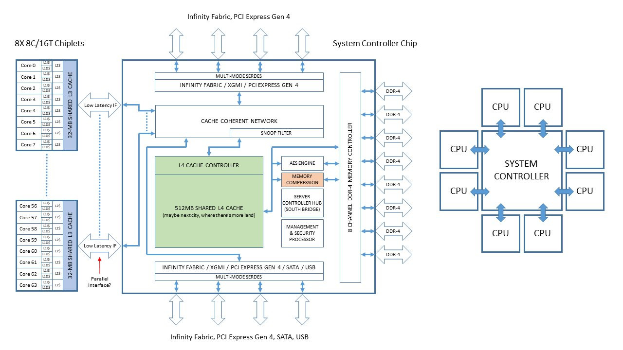
AMD sprung back to competitiveness in the datacenter market with its EPYC enterprise processors, which are multi-chip modules of up to four 8-core dies. Each die has its own integrated northbridge, which controls 2-channel DDR4 memory, and a 32-lane PCI-Express gen 3.0 root complex. In applications that can not only utilize more cores, but also that are memory bandwidth intensive, this approach to non-localized memory presents design bottlenecks. The Ryzen Threadripper WX family highlights many of these bottlenecks, where video encoding benchmarks that are memory-intensive see performance drops as dies without direct access to I/O are starved of memory bandwidth. AMD's solution to this problem is by designing CPU dies with a disabled northbridge (the part of the die with memory controllers and PCIe root complex). This solution could be implemented in its upcoming 2nd generation EPYC processors, codenamed "Rome."

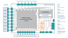
With its "Zen 2" generation, AMD could develop CPU dies in which the integrated northrbidge can be completely disabled (just like the "compute dies" on Threadripper WX processors, which don't have direct memory/PCIe access relying entirely on InfinityFabric). These dies talk to an external die called "System Controller" over a broader InfinityFabric interface. AMD's next-generation MCMs could see a centralized System Controller die that's surrounded by CPU dies, which could all be sitting on a silicon interposer, the same kind found on "Vega 10" and "Fiji" GPUs. An interposer is a silicon die that facilitates high-density microscopic wiring between dies in an MCM. These explosive speculative details and more were put out by Singapore-based @chiakokhua, aka The Retired Engineer, a retired VLSI engineer, who drew block diagrams himself.
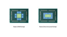
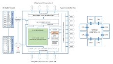
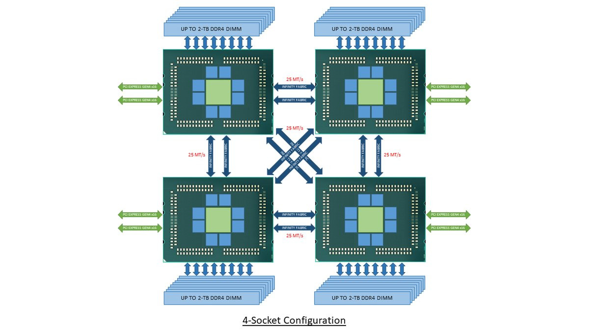
The System Controller die serves as town-square for the entire processor, and packs a monolithic 8-channel DDR4 memory controller that can address up to 2 TB of ECC memory. Unlike current-generation EPYC processors, this memory interface is truly monolithic, much like Intel's implementation. The System Controller also features a PCI-Express gen 4.0 x96 root-complex, which can drive up to six graphics cards with x16 bandwidth, or up to twelve at x8. The die also integrates the southbridge, known as Server Controller Hub, which puts out common I/O interfaces such as SATA, USB, and other legacy low-bandwidth I/O, in addition to some more PCIe lanes. There could still be external "chipset" on the platform that puts out more connectivity.
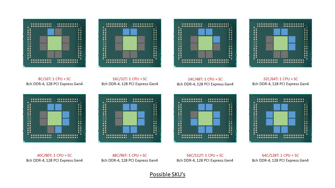
The Retired Engineer goes on to speculate that AMD could even design its socket AM4 products as MCMs of two CPU dies sharing a System Controller die; but cautioned to take it with "a bowl of salt." This is unlikely given that the client-segment has wafer-thin margins compared to enterprise, and AMD would want to build single-die products - ones in which the integrated northbridge isn't disabled. Still, that doesn't completely discount the possibility of a 2-die MCM for "high-margin" SKUs that AMD can sell around $500. In such cases, the System Controller die could be leaner, with fewer InfinityFabric links, a 2-channel memory I/O, and a 32-lane PCIe gen 4.0 root.

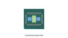
AMD will debut the "Rome" MCM within 2018.
Source: The Retired Engineer
Add your own comment

60 Comments on AMD Could Solve Memory Bottlenecks of its MCM CPUs by Disintegrating the Northbridge

#1
ShurikN
This could also be relevant to the article
Posted on Reply
#2
XiGMAKiD
It's a solution that creates more problems :kookoo:
Posted on Reply
#3
hat
Enthusiast
Hrm... I don't think we've really had multi die chips since Core 2... and since then, the northbridge has moved off the board onto the chip. Still, creating a separate design for EPYC (or even some Threadripper chips) to work around that performance penalty kinda ruins the scalability of the Zen architecture, and may not perform all that well anyway... cause now you've got X amount of dies trying to communicate with the same northbridge, and thereby the rest of the system, at the same time...
Posted on Reply
#4
CheapMeat
This is similar to IBM's approach from what I recall seeing. The SC is the system controller chip. I really like how AMD is trying something else especially with their infinity fabric. I think IBM even helped them with their hyper-threading implementation.

It also makes sense that initially Ryzen and EPYC were based off the same design overall and packaging to save cost and now most likely will separate into their own dedicated production lines.

Posted on Reply
#5
R0H1T
I was wondering when this rumor would end up here, lo & behold. What's interesting is that if the system controller is moved off die, you can basically make any number of CPU/GPU combinations as well, the only limiting factor being the TDP especially for ULV segment. The details should be revealed sometime next month I believe.
hatHrm... I don't think we've really had multi die chips since Core 2... and since then, the northbridge has moved off the board onto the chip. Still, creating a separate design for EPYC (or even some Threadripper chips) to work around that performance penalty kinda ruins the scalability of the Zen architecture, and may not perform all that well anyway... cause now you've got X amount of dies trying to communicate with the same northbridge, and thereby the rest of the system, at the same time...
This isn't just the NB, remember Zen is already a full on SoC.
Posted on Reply
#6
WikiFM
As I kept reading I realized that this is not going to work on the same slow InfinityFabric, also it is going to be more latency because more hops are needed to communicate with cores in another die and also there is not direct access to memory in any die. I can imagine this design to be very low performing in low threaded apps and to have a outrageous power consumption. I hope AMD do not take this approach (good for even more cores, bad for performance)
Posted on Reply
#7
R0H1T
WikiFMAs I kept reading I realized that this is not going to work on the same slow InfinityFabric, also it is going to be more latency because more hops are needed to communicate with cores in another die and also there is not direct access to memory in any die. I can imagine this design to be very low performing in low threaded apps and to have a outrageous power consumption. I hope AMD do not take this approach (good for even more cores, bad for performance)
I have a feeling you'll be surprised (disappointed?) by how well it performs.
www.hpcwire.com/2018/10/30/cray-unveils-shasta-lands-nersc-9-contract/

There's also a possibility that there will be more than one die, especially for desktops & notebooks.
Posted on Reply
#8
WikiFM
R0H1TI have a feeling you'll be surprised (disappointed?) by how well it performs.
www.hpcwire.com/2018/10/30/cray-unveils-shasta-lands-nersc-9-contract/

There's also a possibility that there will be more than one die, especially for desktops & notebooks.
100 petaflops of "peak performance" powered by an undisclosed number of AMD EPYC and NVIDIA GPUs. I'm quite sure most of the performance comes from GPUs anyway. This proves nothing.
Posted on Reply
#9
R0H1T
WikiFM100 petaflops of "peak performance" powered by an undisclosed number of AMD EPYC and NVIDIA GPUs. I'm quite sure most of the performance comes from GPUs anyway. This proves nothing.
It certainly proves that the system isn't bottle-necked in any way you're thinking it'd be, also it's Rome.

You mean "theoretical peak FLOPS" unless we are to believe that CPUs in most supercomputers are just for show.
Posted on Reply
#10
Prima.Vera
So many experts here in CPU design it's amazing to be part of such a group. You should all be hired by AMD! Seriously!

For their "Clown Division"...
Posted on Reply
#11
First Strike
The only question now is whether the 32MB L3 cache per CCX chip will be present as this leak suggests. It is totally possible that L3 cache all get dumped to the center controller chip. 32MB cache in 7nm is really some cost to consider. And making 8 of them shared and coherent is hard AF. If this is the case (and they use it in MSDT), it's screwed.
Posted on Reply
#12
jigar2speed
Prima.VeraSo many experts here in CPU design it's amazing to be part of such a group. You should all be hired by AMD! Seriously!

For their "Clown Division"...
I couldn't have put it better without sounding like a troll.
Posted on Reply
#13
hat
Enthusiast
R0H1TI was wondering when this rumor would end up here, lo & behold. What's interesting is that if the system controller is moved off die, you can basically make any number of CPU/GPU combinations as well, the only limiting factor being the TDP especially for ULV segment. The details should be revealed sometime next month I believe.This isn't just the NB, remember Zen is already a full on SoC.
If the system controller/NB is moved off die... isn't that a huge step backwards? Sure it might be good for connecting a lot of stuff together... but it would be really slow and clunky compared to the way things have been done for the past 10 years or more.

Anyway, this design (and others that exist already, as seen in the 2990WX) kinda sounds like a multi socket system... all in one chip. It's great for huge threaded workloads, being wallet friendly, and cramming an obscene amount of cores into one chip/board, but if you're not using it for that, it's detrimental.
Posted on Reply
#14
R0H1T
hatIf the system controller/NB is moved off die... isn't that a huge step backwards? Sure it might be good for connecting a lot of stuff together... but it would be really slow and clunky compared to the way things have been done for the past 10 years or more.

Anyway, this design (and others that exist already, as seen in the 2990WX) kinda sounds like a multi socket system... all in one chip. It's great for huge threaded workloads, being wallet friendly, and cramming an obscene amount of cores into one chip/board, but if you're not using it for that, it's detrimental.
That's the biggest question for everyone right now, though if the leaks are true then AMD must have done their own tests & found it to not be such a major regression, if at all. The part about L3 & possible L4 also makes sense, as some of the latency trade-offs can be mitigated by increasing the L3 size & introducing L4 thereby increasing the overall cache hits.

I think there will be more dies this time around, Zen had 2 with the second one being RR having an IGP.
Posted on Reply
#15
hat
Enthusiast
Maybe you're on to something. When the Athlon was smacking the Pentium around, part of the reason for that was because they had an on die memory controller... but then the Core 2 series came out, and though it still relied on the old, slow FSB (with memory controller on the then on board, not on chip NB), it smacked the Athlon around... and they had big caches. Then Intel had much smaller caches with Nehalem, going forward.

AMD's CCX design is great, but even that has its limits, as when you put a bunch of them together, they all have to communicate with each other in some way... but there was a reason everything moved off the board onto the CPU, it's much faster that way. AMD certainly has an issue on their hands... and this move seems like a gamble to me. Time will tell if they come out with a hit of a flop...
Posted on Reply
#16
WikiFM
Prima.VeraSo many experts here in CPU design it's amazing to be part of such a group. You should all be hired by AMD! Seriously!

For their "Clown Division"...
Did you already notice that you included yourself? :laugh:
Posted on Reply
#17
ShurikN
Prima.VeraSo many experts here in CPU design it's amazing to be part of such a group. You should all be hired by AMD! Seriously!

For their "Clown Division"...
Took the words out of my mouth... or fingers in this case.
Posted on Reply
#18
generaleramon
AMD knew what it was doing with Zen and the CCX/Infinity Fabric thing(i guess we can agree that Zen is overall a good and performing architecture), now, i guess they have learned something from this experience and they want to go further with the idea, also... the multi chip solution is the only practical one we have for high core count cpus, there is no way to manifacture gigantic peaces of silicon with decent yealds. And we also don't know if AMD made some improvements to the Infinty Fabric to reduce the bandwidth/latency problem of this connection, other than increasing the L3 cache for obvious reasons. I think this is something new, with good possibilities if done correctly, we need to relax and wait for the end result. As costumers/consumers, we always need to be positive and supportive for new and brave ideas.
Posted on Reply
#19
PanicLake
XiGMAKiDIt's a solution that creates more problems :kookoo:
It's a comment that provides no argument...
Posted on Reply
#20
sergionography
But how does this effect minimum latency? Right now with the current approach there is a somewhat wide delta between min and max latency depending on which core is communicating with what. When an app is running locally on a ccx the latency is excellent, when both ccx's are needed then the latency slightly increases, and lastly when needing to connect to other chips on the module for one workload then latency maxes out. This central north bridge might lower that max latency and make the gap between min and max much smaller, however from a high level one can expect min latency to take a big hit and increase drastically.

Tldr - Unless i am misunderstanding something; this approach will only lower the min-max delta to make a more consistent latency in all workloads, but that would be achieved by increasing min latency and decreasing max latency - counter productive if true
Posted on Reply
#21
Zubasa
sergionographyBut how does this effect minimum latency? Right now with the current approach there is a somewhat wide delta between min and max latency depending on which core is communicating with what. When an app is running locally on a ccx the latency is excellent, when both ccx's are needed then the latency slightly increases, and lastly when needing to connect to other chips on the module for one workload then latency maxes out. This central north bridge might lower that max latency and make the gap between min and max much smaller, however from a high level one can expect min latency to take a big hit and increase drastically.

Tldr - Unless i am misunderstanding something; this approach will only lower the min-max delta to make a more consistent latency in all workloads, but that would be achieved by increasing min latency and decreasing max latency - counter productive if true
Currently the Zen die compose of 2 CCX of Quad-Cores and both are connected to the SOC / NB via Infinity Fabric.
So to access the L3 Cache that is on another die it requires 3 hops, first from the CCX to the local SOC, second to SOC of the other die, then from the other SOC to the CCX with the L3.
On this new layout the number of hops is 2, first to the Central Hub, second to the other CCX where the L3 is located.

What this does though, is avoid the issues with the 2990WX / 2970WX where some cores needs 3 hops to the memory.
First from CCX to local SOC then to the SOC on the IO Die.
Also the 2-Die Threadripper connects to each other via 2 links of Infinity Fabric, and the 4-Die version only has 1 connection to each die, so half the bandwidth.
If each Zen 2 die also keeps its 2 IF links, it would always have as much if not double bandwidth to the memory, if AMD can keep the IF speed the same as Zen 1.
On Zen 2 each CCX is always 1 hop away from memory, meaning it will have consistent latency across all dies.

For gaming isn't it mostly the maximum latency that cause frame-time issues?
After all the 1% and 0.1% lows are measuring the max frame time between each frame, as the minimum frame time aka Max FPS isn't nearly as important.
Posted on Reply
#22
bug
XiGMAKiDIt's a solution that creates more problems :kookoo:
It's engineering. Any solution will create problems sooner or later, given the "proper" scenario ;)
Posted on Reply
#23
Vya Domus
First StrikeThe only question now is whether the 32MB L3 cache per CCX chip will be present as this leak suggests. It is totally possible that L3 cache all get dumped to the center controller chip. 32MB cache in 7nm is really some cost to consider. And making 8 of them shared and coherent is hard AF. If this is the case (and they use it in MSDT), it's screwed.
The cache needs to be low latency, therefore it has to be on the same die.
WikiFMbecause more hops are needed to communicate with cores in another die
It's going to be less actually, on average.
WikiFMI can imagine this design to be very low performing in low threaded apps
If the communication between the cores is hampered as you say , how would that affect the single thread performance ? It's the exact opposite of what you are describing, leaving only the cores and cache on each die would allow for higher clocks and therfore higher single thread performance and higher performance in general.
Posted on Reply
#24
Vayra86
So, all roads truly do lead to Rome, then.
Posted on Reply
#25
bug
Vayra86So, all roads truly do lead to Rome, then.
More like many Romes will lead to one road instead ;)
Posted on Reply
Add your own comment
Apr 26th, 2024 12:08 EDT change timezone

New Forum Posts

Popular Reviews

Controversial News Posts