Jun 1st, 2025 23:32 EDT
change timezone
Latest GPU Drivers
New Forum Posts
- Opinions on AI (450)
- [TT] AMD rumored Radeon RX 9080 XT: up to 32GB of faster GDDR7, up to 4GHz GPU clocks, 450W power (49)
- AAF Optimus Modded Driver For Windows 10 & Windows 11 - Only for Realtek HDAUDIO Chips (498)
- Windows 11 General Discussion (6041)
- Why don't cases seperate CPU from GPU for thermal reasons? (11)
- 6800xt va 4070 12gb (49)
- Ghetto Mods (4578)
- ASUS Zephyrus Duo 16 (GX650PY) – RTX 4090 GPU Driver Issues, Black Screen, Artifacting, and Freezing Post-Clean Install (Help Needed) (1)
- 6700 XT vs. RTX 3070 for 1080p resolution - Seeking urgent help, details inside. (8)
- Are The "Newer" NVIDIA GPU Driver Series Now Good Enough To Install (Bugs Fixed?) (8)
Popular Reviews
- NVIDIA GeForce RTX 5060 8 GB Review
- ASUS Radeon RX 9070 XT TUF OC Review
- Lian Li Lancool 217 Review
- Upcoming Hardware Launches 2025 (Updated May 2025)
- DOOM: The Dark Ages Performance Benchmark Review - 40 GPUs Tested
- AMD Ryzen 7 9800X3D Review - The Best Gaming Processor
- Sapphire Radeon RX 9070 XT Nitro+ Review - Beating NVIDIA
- MSI MAG X870E Tomahawk Wi-Fi Review
- Clair Obscur: Expedition 33 Performance Benchmark Review - 33 GPUs Tested
- Phylina S480 Max Review
TPU on YouTube

Controversial News Posts
- AMD Announces Radeon RX 9060 XT Graphics Card, Claims "Fastest Under $350" (139)
- Microsoft Forces Automatic Windows 11 24H2 Update on Pro and Home PCs (121)
- XFX & Acer Radeon RX 9060 XT Graphics Cards Leaked by Retailers - Starting at "$450" (120)
- AMD "Zen 7" Rumors: Three Core Classes, 2 MB L2, 7 MB V‑Cache, and TSMC A14 Node (98)
- NVIDIA's GeForce RTX 5080 SUPER Gains 24 GB GDDR7, Keeps 10,752 CUDA Cores (88)
- NVIDIA Issues vBIOS Update to Fix RTX 5060 (Ti) Reboot Black Screens (72)
- NVIDIA Announces Financial Results for First Quarter Fiscal 2026 (68)
- Intel Partner Prepares Dual Arc "Battlemage" B580 GPU with 48 GB of VRAM (64)
Tuesday, September 3rd 2019

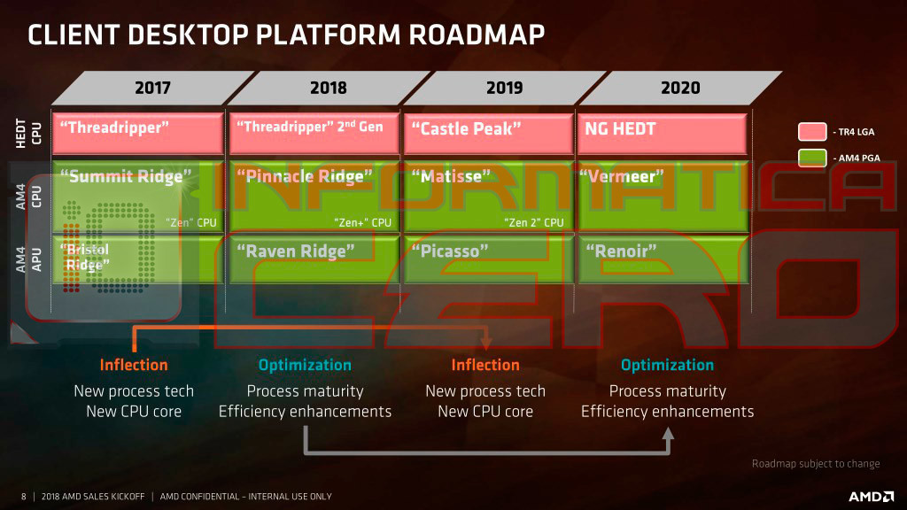
AMD "Renoir" APU to Support LPDDR4X Memory and New Display Engine
AMD's next-generation "Renoir" APU, which succeeds the company's 12 nm "Picasso," will be the company's truly next-generation chip to feature an integrated graphics solution. It's unclear as of now, if the chip will be based on a monolithic die, or if it will be a multi-chip module of a 7 nm "Zen 2" chiplet paired with an enlarged I/O controller die that has the iGPU. We're getting confirmation on two key specs - one, that the iGPU will be based on the older "Vega" graphics architecture, albeit with an updated display engine to support the latest display standards; and two, that the processor's memory controller will support the latest LPDDR4X memory standard, at speeds of up to 4266 MHz DDR. In comparison, Intel's "Ice Lake-U" chip supports LPDDX4X up to 3733 MHz.
Code-lines pointing toward "Vega" graphics with an updated display controller mention the new DCN 2.1, found in AMD's new "Navi 10" GPU. This controller supports resolutions of up to 8K, DSC 1.2a, and new resolutions of 4K up to 240 Hz and 8K 60 Hz over a single cable, along with 30 bits per pixel color. The multimedia engine is also suitably updated to VCN 2.1 standard, and provides hardware-accelerated decoding for some of the newer video formats, such as VP9 and H.265 at up to 90 fps at 4K, and 8K up to 24 fps, and H.264 up to 150 fps at 4K. There's no word on when "Renoir" comes out, but a 2020 International CES unveil is likely.
Source:
Phoronix
Code-lines pointing toward "Vega" graphics with an updated display controller mention the new DCN 2.1, found in AMD's new "Navi 10" GPU. This controller supports resolutions of up to 8K, DSC 1.2a, and new resolutions of 4K up to 240 Hz and 8K 60 Hz over a single cable, along with 30 bits per pixel color. The multimedia engine is also suitably updated to VCN 2.1 standard, and provides hardware-accelerated decoding for some of the newer video formats, such as VP9 and H.265 at up to 90 fps at 4K, and 8K up to 24 fps, and H.264 up to 150 fps at 4K. There's no word on when "Renoir" comes out, but a 2020 International CES unveil is likely.
Jun 1st, 2025 23:32 EDT
change timezone
Latest GPU Drivers
New Forum Posts
- Opinions on AI (450)
- [TT] AMD rumored Radeon RX 9080 XT: up to 32GB of faster GDDR7, up to 4GHz GPU clocks, 450W power (49)
- AAF Optimus Modded Driver For Windows 10 & Windows 11 - Only for Realtek HDAUDIO Chips (498)
- Windows 11 General Discussion (6041)
- Why don't cases seperate CPU from GPU for thermal reasons? (11)
- 6800xt va 4070 12gb (49)
- Ghetto Mods (4578)
- ASUS Zephyrus Duo 16 (GX650PY) – RTX 4090 GPU Driver Issues, Black Screen, Artifacting, and Freezing Post-Clean Install (Help Needed) (1)
- 6700 XT vs. RTX 3070 for 1080p resolution - Seeking urgent help, details inside. (8)
- Are The "Newer" NVIDIA GPU Driver Series Now Good Enough To Install (Bugs Fixed?) (8)
Popular Reviews
- NVIDIA GeForce RTX 5060 8 GB Review
- ASUS Radeon RX 9070 XT TUF OC Review
- Lian Li Lancool 217 Review
- Upcoming Hardware Launches 2025 (Updated May 2025)
- DOOM: The Dark Ages Performance Benchmark Review - 40 GPUs Tested
- AMD Ryzen 7 9800X3D Review - The Best Gaming Processor
- Sapphire Radeon RX 9070 XT Nitro+ Review - Beating NVIDIA
- MSI MAG X870E Tomahawk Wi-Fi Review
- Clair Obscur: Expedition 33 Performance Benchmark Review - 33 GPUs Tested
- Phylina S480 Max Review
TPU on YouTube
Controversial News Posts
- AMD Announces Radeon RX 9060 XT Graphics Card, Claims "Fastest Under $350" (139)
- Microsoft Forces Automatic Windows 11 24H2 Update on Pro and Home PCs (121)
- XFX & Acer Radeon RX 9060 XT Graphics Cards Leaked by Retailers - Starting at "$450" (120)
- AMD "Zen 7" Rumors: Three Core Classes, 2 MB L2, 7 MB V‑Cache, and TSMC A14 Node (98)
- NVIDIA's GeForce RTX 5080 SUPER Gains 24 GB GDDR7, Keeps 10,752 CUDA Cores (88)
- NVIDIA Issues vBIOS Update to Fix RTX 5060 (Ti) Reboot Black Screens (72)
- NVIDIA Announces Financial Results for First Quarter Fiscal 2026 (68)
- Intel Partner Prepares Dual Arc "Battlemage" B580 GPU with 48 GB of VRAM (64)
39 Comments on AMD "Renoir" APU to Support LPDDR4X Memory and New Display Engine
Raven Ridge's CPU portion has no advantages over the equivalent i7 (slower, hungrier, lower IPC) and it sucks that AMD doesn't provide software to control the APUs properly. We rely on third parties for that.
One thing I found helpful for gaming was to run the game with processor affinity limited to two consecutive threads (one physical core with SMT). Assuming the game runs on two threads, it's usually an improvement in IGP performance. Just create a shortcut to your game with the following:
cmd.exe /c start "Program Name" /affinity 3 "Full path of application file"
The 3 is hexdecimal for 11, implying core0 and core1 are active.
affinity 1 = 1C/1T
affinity 3 = 1C/2T
affinity 5 = 2C/2T
affinity 1E = 2C/4T
I don't think there's any point going higher than that because the IGP will always be the gaming bottleneck even with only 2C/4T active.
There is less CPU usage then (especially when hardware acceleration is present).
Hexadecimal 3 is... 3.
- AMD can make Navi work with an APU, but they don't want to provide a GPU solution in the APU that makes casual gamers just skip a discrete AMD GPU when building their computer.
- AMD developed Navi with Sony and Microsoft money and there's some provision that AMD can't use Navi in APUs until after console release so as not to overshadow the custom APUs.
- AMD is out of time and money to make Navi work with the APUs that aren't really their profit center right now.
- The GPU part is going to be integrated into the IO chip and Navi was never validated on the larger lithography.
Whatever the case, AMD will be looking pretty weak on APU performance if Intel is able to push out Gen 11 integrated graphics on their chips anytime soon. Hopefully they figured out some way to up the number of compute units to at least beat the existing chips in graphics performance.Note that the Vega chip in those implementations has its own dedicated HBM2 framebuffer, removing the need to share bandwith with the CPU.
If you compare the Vega 8 in the 2200g with the Vega 11 in the 2400g, there is a 50% increase in raw power, but the gaming performance is really close. Shure, "Renoir" has potentially higher ram speeds (4266 MHz compared to 3200 MHz) but that is peanuts (68 GB/s and 51 GB/s) compared to the dedicated bandwidth of the 8809g at over 200 GB/s.
In short; memory interface speed is holding AMD APUs back, and nothing short of a dedicated HMB2 chip for GPU memory on package will solve that.
TSMC's 7nm node is busy. Everyone wants a piece, not just AMD. So AMD have limited 7nm capacity available to them and all of that is going on Zen chiplets for Epyc in the case of the most efficient yields (where the profit margin is 10x what it is in the consumer space) and the leakier, higher-voltage chips become consumer Ryzen.
This is why the only Navi parts coming out right now are going into the high-end market. There's not enough spare 7nm production capacity to justify making low-end consumer parts with tiny profit margins, so the only APUs we're likely to see in the immediate future are probably going to be 8C/16T Zen2 chiplets that are super-defective but can be salvaged as 4C/8T. All AMD have to do to make Renoir from those is throw them onto a package with existing Vega and IO controller made on the cheap and unconstrained GloFo 14nm process.
Additionally, both of them have memory in the same ballpark as the HBM2 chip in the 8809g for the GPUs (Xbox one x 326 GB/s and PS4 is 176 GB/s)
The Subor Z+ sits at 256 GB/s according to this.
I still think it’s a question of memory bandwidth for the consumer APUs from AMD.