Monday, January 4th 2021

AMD Patents Chiplet Architecture for Radeon GPUs
On December 31st, AMD's Radeon group has filed a patent for a chiplet architecture of the GPU, showing its vision about the future of Radeon GPUs. Currently, all of the GPUs available on the market utilize the monolithic approach, meaning that the graphics processing units are located on a single die. However, the current approach has its limitations. As the dies get bigger for high-performance GPU configurations, they are more expensive to manufacture and can not scale that well. Especially with modern semiconductor nodes, the costs of dies are rising. For example, it would be more economically viable to have two dies that are 100 mm² in size each than to have one at 200 mm². AMD realized that as well and has thus worked on a chiplet approach to the design.
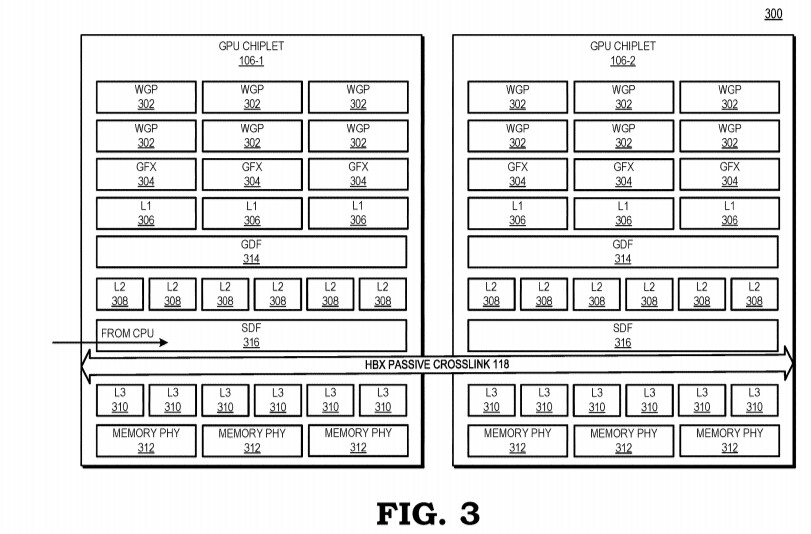
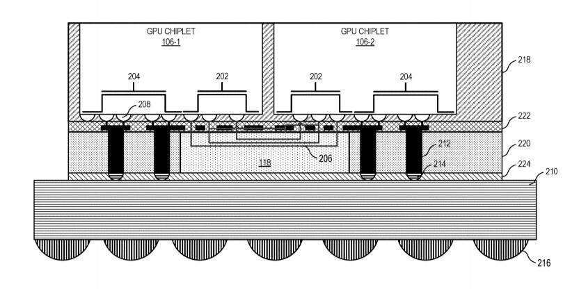
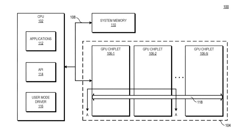
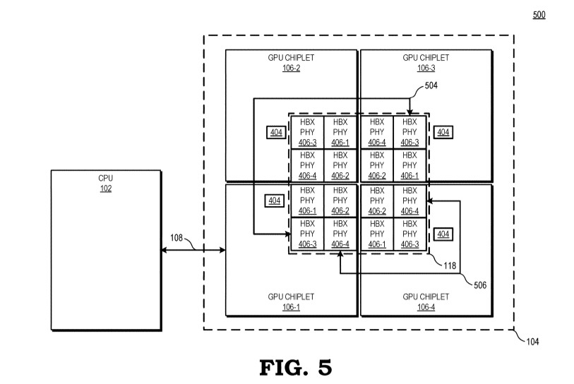
AMD reports that the use of multiple GPU configuration is inefficient due to limited software support, so that is the reason why GPUs were kept monolithic for years. However, it seems like the company has found a way to go past the limitations and implement a sufficient solution. AMD believes that by using its new high bandwidth passive crosslinks, it can achieve ideal chiplet-to-chiplet communication, where each GPU in the chiplet array would be coupled to the first GPU in the array. All the communication would go through an active interposer which would contain many layers of wires that are high bandwidth passive crosslinks. The company envisions that the first GPU in the array would communicably be coupled to the CPU, meaning that it will have to use the CPU possibly as a communication bridge for the GPU arrays. Such a thing would have big latency hit so it is questionable what it means really.
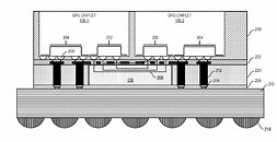
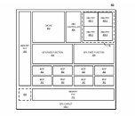
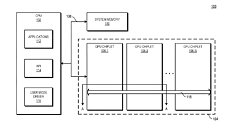 The patent also suggests that each GPU chiplet uses its own Last Level Cache (LLC), instead of separate LLCs for each GPU, so each of the LLCs is communicably coupled and the cache remains coherent across all chiplets. Rumors suggest that we are going to see the first chiplet-based architecture from AMD as successor to the RDNA3 generation, so it will happen in the coming years. AMD already has experience with chiplets from its processors, with Ryzen processors being the prime example. We just need to wait and see how it will look once it arrives for GPUs.
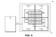
Sources:
Free Patents Online, via VideoCardz
AMD reports that the use of multiple GPU configuration is inefficient due to limited software support, so that is the reason why GPUs were kept monolithic for years. However, it seems like the company has found a way to go past the limitations and implement a sufficient solution. AMD believes that by using its new high bandwidth passive crosslinks, it can achieve ideal chiplet-to-chiplet communication, where each GPU in the chiplet array would be coupled to the first GPU in the array. All the communication would go through an active interposer which would contain many layers of wires that are high bandwidth passive crosslinks. The company envisions that the first GPU in the array would communicably be coupled to the CPU, meaning that it will have to use the CPU possibly as a communication bridge for the GPU arrays. Such a thing would have big latency hit so it is questionable what it means really.


69 Comments on AMD Patents Chiplet Architecture for Radeon GPUs
Having independent GPCs made a lot more sense but it was probably more complicated on the host side to distribute commands.
I remember the 4870 X2 where it was 2 chips on 1 pcb connected with a PLX chip or something?
Chiplet based CPUs are also far better for binning. Compared to a monolithic design where a single defect can reduce the value of the entire die, with chiplets you can just bin the best dies for the best CPUs. With chiplets you also get to pick which specific dies to use in each specific CPU model. This is what allows AMD to make CPUs like the 5950X. They are cherry picking the best dies to achieve a lower power consumption and higher performance.
Other reasons also include cost and yield. Suffice it to say, implying that AMD adopted chiplets only because it was cost effective is misleading. I think it's pretty clear AMD knew this design's other advantages from the onset.
www.eecg.utoronto.ca/~enright/modular-isca.pdf
and a quick summary
www.cs.ucy.ac.cy/conferences/pact2018/material/PACT2008-public.pdf
Memory is global: all CUs on a GPU (like MI100 or RDNA2) have the potential to access any memory location. Now, L2 caches are pretty smart: the L2 cache could be pulling from PCIe 4.0 (aka: CPU RAM), and the CUs are none-the-wiser. But keeping that data in-sync across a GPU is very important within a ROCm or OpenCL kernel. Heck, even across kernels, you may share some VRAM and keeping those views consistent requires a bit of effort. (Mostly because L1 caches aren't very coherent on GPUs... so you need to worry about keeping Constant-L1 vs __shared__ vs Vector-L1 in sync).
On AMD architectures at least, the memory model seems to be coherency in the L2 cache. But if you split things up between chiplets, you're going to have separate L2 caches, and things are going to get a LOT more complicated. I can't think of any automated way of keeping separate L2 caches in sync: the programmer simply has to adapt to the new architecture. Maybe some "easy cases" can be detected (two kernels touching two different memory sets independently)... but its non-obvious to me how that kind of system would work.
Alternatively: AMD could keep L2 caches coherent by creating a very large-and-bulky communication mechanism between L2 caches (a "GPU Infinity Fabric"). Which is what this patent appears to be doing with that HBX-crosslink.
Hmmm... L3 cache? That's different. RDNA is L0, L1, and L2 (where L1 and L2 are in the proper place in the above diagram). L3 is new.
-------
I don't quite remember the last time we talked about this issue. But I'll bring up the same "Framebuffer" issue as before: the "Framebuffer" is the final rendering of any image on the GPU: the sum of transparency / fog / rasterization / raytracing / all results right before it enters the monitor. The Framebuffer is a hard-hit portion of RAM which must be shared and even has some order-dependent effects going on (transparency is strongly ordered: A (80% alpha) on top of B (50% alpha) on top of C will result in a grossly different picture of C on top of B on top of A). That's the kind of memory sync and memory sharing that happens every render of every frame in every video game.
Geometry shaders will read and write all the data in parallel. Then when the vertex shaders run after those, they'll all read and write the data together. Finally, pixel shaders process the data all in parallel and eventually deposit their results into the framebuffer.
Yeah I'm skipping a few steps, but that's the gist of it. A modern GPU shares a lot of information in parallel. At a minimum, all of those shaders are performing shared reads, and there needs to be a synchronization point where all of that data is merged together (especially because any transparency algorithm must be Z-order sorted and then applied from furthest-away to closest ala the Painter's algorithm).
There's only one framebuffer (maybe two if you're playing VR for your two eyes: but those two framebuffers must remain in sync regardless). Any geometry shader which tessellates... any vertex shader custom-animation thing... any shared data at all must be synchronized across all compute units. There's only one mipmapped copy of Gordon Freeman's face in VRAM, and that copy is shared to all wavefronts that may want to render any piece of Gordon Freeman's face (texture, vertex, tessellation data).
-------
There's a reason why Crossfire and SLI failed: the data synchronization issue is actually pretty difficult to solve. There was a time when we thought that simple data-sharing patterns was good enough... but as effects got more complicated (more transparency, more sharing of shadows, more complicated tessellation patterns or whatever), the more and more important data-sharing became.
I'm not saying this data-synchronization problem is unsolvable, but there's a reason why AMD is putting a big fat "HBX Crosslink" between their chiplets in this patent. Maybe this HBX-crosslink is good enough, or maybe not. AMD is surely going to build a prototype now (if they haven't already). If its good enough, maybe we'll see it in a product in a few years. If not, then it will be tossed into the trashbin and another design will be made.
-------
EDIT: I realize I'm still being handwavy. Here's a specific example which clearly relies upon shared-data states: Claybook (gpuopen.com/wp-content/uploads/2018/05/gdc_2018_tutorial_clay_sim_and_raytracing_in_claybook.pptx).
Youtube:
The physics + fluids of Claybook were implemented on the GPU. Its clear that the world-state (where tracks are, for example) is shared between all parallel processors and that various parts of the scene (shadows, verticies, etc. etc.) morph to that shared state.
NIiiiiiiiiice!
Dx12 mGPU implicit been around for years, and theoretically can present just one GPU for system with multi adapters and yet none of developer take advantages of it. Just like what you said, a prime example of EA's Battlefield, I can run Battlefield 1 with Vega 56 Crossfire and suddenly borked in Battlefield V even though it needs more of GPU power. Several matter could come into hands, the most obvious is temporal anti aliasing will not work and developer need to write another thousand rows of code. These approach would eliminating API needed and bloated codes as hardware itself is controlling it.
Still, this is too much for average joe like me, I mean you could "easily" parallel a serial processor ( chiplet design on Ryzen CPU ), but what it takes to parallel already parallel processor ( GPU ), or arrange all those parallel processor as serial? :confused:
But I have to point out again that if every wavefront needing to fetch something would require synchronization the performance implications would be ridiculous.
Atomic reads/writes to the same locations in memory. Some of it is optimized to an atomic read/write to __local__ memory, but some of it must happen globally synchronized.
That's a global write across compute units being consolidated into the same memory locations. The only way to synchronize that effectively is through atomic operations, which modern GPUs can actually do very quickly.
------
Its hard to come up with a single example, because most examples of writing to the same memory location are considered trivial. I don't think people talk about it because its happening all the freaking time. That's the very reason atomics + memory barriers are implemented on modern GPUs.
The hard part is finding ways to localize and minimize the naive approach. The Claybook devs have noted a lot of areas where they were able to synchronize to __local__ or __shared__ memory instead (which is much faster for this kind of stuff). But that doesn't change the fact that the ultimate data must be synchronized to the global state eventually... and such synchronization is going to happen in different CUs.
I dunno, do you need to see the simpler programming examples to believe me?
on-demand.gputechconf.com/gtc/2013/presentations/S3101-Atomic-Memory-Operations.pdf
Is there a good reason for them to use the same design on the gpu as the cpu, or are they just stroking themselves because it seems to be working so well on the cpu's?
Is there actually an advantage to this on the gpu? why is monolithic gpu design suddenly cack? or is everyone gonna just go hoorah for Amd as Intel are now the "underdog"
And they are dog slow by the way for that reason.
My point remains: there are global data-structures on GPUs that must remain synchronized. Currently, that synchronization mechanism is L2 cache atomics. Your proposal to split the data between chiplets ignores the synchronization mechanism of typical GPU code.
"Render Texture" in modern game engines (see docs.unity3d.com/Manual/class-RenderTexture.html) is another situation where multiple CUs have to write to the same memory (or at least: the same texture). You almost certainly want to render that texture as parallel as possible. From my understanding, render-to-texture at runtime is used in all sorts of advanced effects (blog.theknightsofunity.com/practical-use-of-render-textures/).
GPU effects on modern video games are now a complex web of dependencies. That's just where the industry has gone in the past 10 years: these sorts of advanced effects are cheap to calculate and look really good.
An example - these die sizes are made up, and I'm assuming linear CU scaling per area here which is a bit on the optimistic side, but reasonably representative. Yield rate is based on published TSMC yield data of 0.09 defects/cm². Yield calculations from here.
-A 15x15mm die (225mm²) fits 256 dice per 300mm wafer with ~46 (partially or fully) defective dice.
-A 15x30mm die (450mm²) fits 116 dice per 300mm wafer with ~38 (partially or fully) defective dice.
In other words halving die size increases dice per wafer by 120%, while defective dice only increase by 21%. In other words you're left with far more fault-free silicon, giving a lot more flexibility in binning and product segmentation. If 10% of error-free dice hit the top clock speed/voltage bin, that's ~7.8 dice per wafer on the larger die or ~21 dice per wafer on the smaller die. If two of the smaller can be combined to work as an equivalent of one of the larger, you then have ~2,7 more useable flagship GPUs per wafer or a 34% increase in yields for the top bin, and far more flexibility for the remainder, seeing how it can be used for either 1- or 2-die configurations, giving a much wider possible range of configurations and thus a higher chance of utilizing faulty dice too (a >50% cut-down SKU of a large die is immensely wasteful and extremely unlikely to happen, after all).
Also, cost goes way down. Assuming a per-wafer cost of $20 000, the smaller die ends up at ~$95/die (not counting defective dice), while the larger die ends up at ~$256 (same). Taking into account the higher likelihood of being able to use the defective dice from the smaller design, that further brings down prices. If 50% of defective small dice can be used vs. 30% of defective large dice, that's ~$86 vs. ~$206.
Nobody is saying monolithic GPU designs are cack, but we're reaching the practical and economical upper limits of monolithic GPU die designs. If we want better performance at even remotely accessible prices in the future, we need new ways of making these chips.
"The prospects of 4 discrete GPU's with a chunk of infinity cache on each running to a CPU with larger chunk of infinity cache that it can split amongst them is a very real future and vastly better than 4-way GTX980/980Ti's was with those old slower and less multicore Intel workstation chips and motherboards like setup is archaic to what we've got now it may as well be a 486 it just looks so dated this current tech in so many area's."