Monday, January 4th 2021

AMD Patents Chiplet Architecture for Radeon GPUs

On December 31st, AMD's Radeon group has filed a patent for a chiplet architecture of the GPU, showing its vision about the future of Radeon GPUs. Currently, all of the GPUs available on the market utilize the monolithic approach, meaning that the graphics processing units are located on a single die. However, the current approach has its limitations. As the dies get bigger for high-performance GPU configurations, they are more expensive to manufacture and can not scale that well. Especially with modern semiconductor nodes, the costs of dies are rising. For example, it would be more economically viable to have two dies that are 100 mm² in size each than to have one at 200 mm². AMD realized that as well and has thus worked on a chiplet approach to the design.

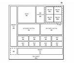
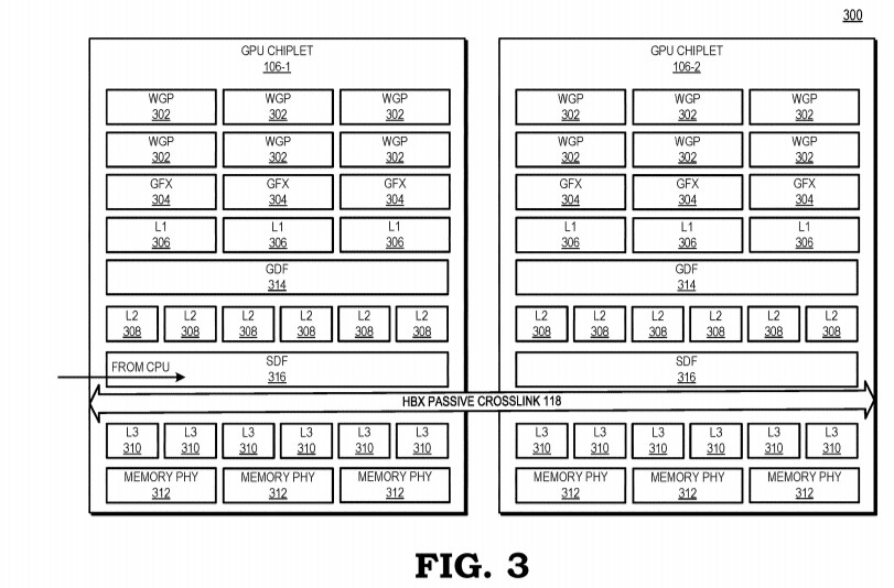
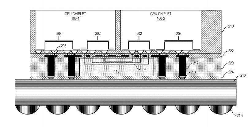
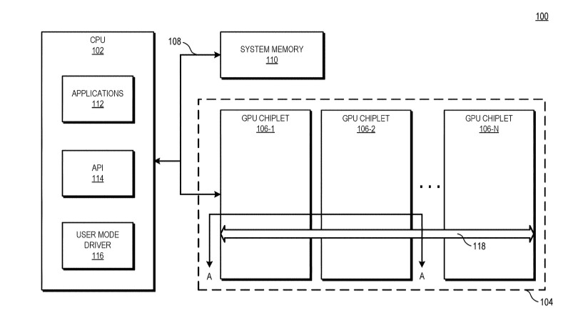
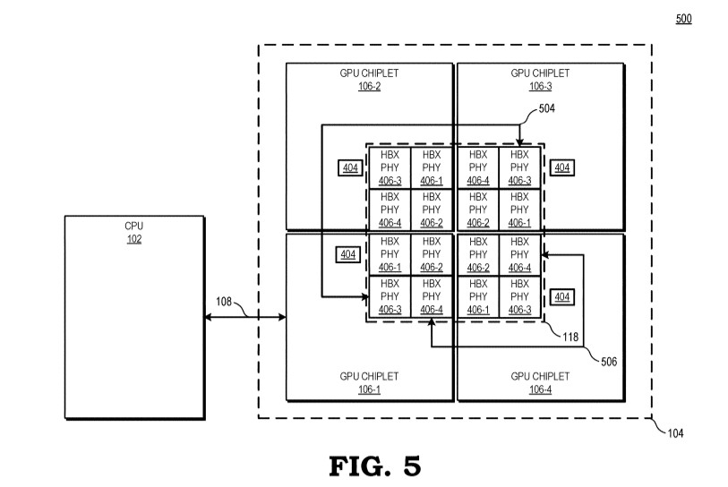
AMD reports that the use of multiple GPU configuration is inefficient due to limited software support, so that is the reason why GPUs were kept monolithic for years. However, it seems like the company has found a way to go past the limitations and implement a sufficient solution. AMD believes that by using its new high bandwidth passive crosslinks, it can achieve ideal chiplet-to-chiplet communication, where each GPU in the chiplet array would be coupled to the first GPU in the array. All the communication would go through an active interposer which would contain many layers of wires that are high bandwidth passive crosslinks. The company envisions that the first GPU in the array would communicably be coupled to the CPU, meaning that it will have to use the CPU possibly as a communication bridge for the GPU arrays. Such a thing would have big latency hit so it is questionable what it means really.
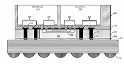
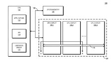
The patent also suggests that each GPU chiplet uses its own Last Level Cache (LLC), instead of separate LLCs for each GPU, so each of the LLCs is communicably coupled and the cache remains coherent across all chiplets. Rumors suggest that we are going to see the first chiplet-based architecture from AMD as successor to the RDNA3 generation, so it will happen in the coming years. AMD already has experience with chiplets from its processors, with Ryzen processors being the prime example. We just need to wait and see how it will look once it arrives for GPUs.
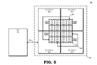
Sources: Free Patents Online, via VideoCardz
Add your own comment

69 Comments on AMD Patents Chiplet Architecture for Radeon GPUs

#51
InVasMani
Well smaller chips are cheaper than a larger monolithic design by a wide margin.
Posted on Reply
#52
Valantar
Gruffalo.SoldierBig question is, will it cost more.
The main reason for doing this is to reduce costs. So no. The interposer will obviously not be cheap, but given sufficient production volume the cost of that will make little difference compared to the savings of making smaller dice. See my calculations a few posts up for a rough estimation.
Posted on Reply
#53
londiste
Cost and chiplet design overhead is also the function of chiplet size and count.
Posted on Reply
#54
Valantar
londisteCost and chiplet design overhead is also the function of chiplet size and count.
True. Designing a cutting-edge chip and getting it mass produced does after all cost from hundreds of millions of USD to billions of USD. If a chiplet design allows them to go from, say, small-medium-large-XL monolithic chips to small+medium chiplets in various combinations, that is a massive R&D and manufacturing savings even when accounting for the R&D needed for interposer development, advanced packaging technologies, etc.
Posted on Reply
#55
AusWolf
Judging by the 20 C difference between edge temp and hotspot temp on my 5700 XT under load, imagine it must be easier to cool a bunch of smaller dies than a single big one.
Posted on Reply
#56
Valantar
AusWolfJudging by the 20 C difference between edge temp and hotspot temp on my 5700 XT under load, imagine it must be easier to cool a bunch of smaller dies than a single big one.
That depends. Getting a single cold plate to make ideal contact with a collection of individual surfaces will always be more difficult than having it make contact with a single surface. Also, edge/hotspot temperature deltas like that are likely found on all high powered chips, it's just rare for them to have a thermal reporting system that allows users to see both. A smaller die is of course likely to pull less power and might have a smaller distance from edge to hotspot, but the difference isn't likely to be huge. The portion of the chip consuming the power will always be hotter than surrounding regions.
Posted on Reply
#57
RainingTacco
So they decreased the chiplet dependency on new ryzens 5000, and they want to introduce similar thing to GPU? Why? Havent they learned about latency...
Posted on Reply
#58
Valantar
RainingTaccoSo they decreased the chiplet dependency on new ryzens 5000, and they want to introduce similar thing to GPU? Why? Havent they learned about latency...
Hm? There are exactly the same amount of chiplets in Ryzen 5000 as Ryzen 3000. They reduced the number of CCXes (Core Complex) per CCD (chiplet, Core Complex Die) from 2 to 1 by doubling the number of cores per CCX, but there are still two CCDs + an IOD in anything with >8 cores and one CCD for anything =<8 cores.
Posted on Reply
#59
RainingTacco
ValantarHm? There are exactly the same amount of chiplets in Ryzen 5000 as Ryzen 3000. They reduced the number of CCXes (Core Complex) per CCD (chiplet, Core Complex Die) from 2 to 1 by doubling the number of cores per CCX, but there are still two CCDs + an IOD in anything with >8 cores and one CCD for anything =<8 cores.
You are right. I thought they've ditched the whole infinity fabric shtick and made unified die. They actually didn't.
Posted on Reply
#60
Valantar
RainingTaccoYou are right. I thought they've ditched the whole infinity fabric shtick and made unified die. They actually didn't.
That's only the APUs, AMD aren't going back to monolithic dice for CPUs, likely not ever. The MCM approach allows them low production costs, high yields, great binning flexibility, easy configurability, and a heap of other advantages. And latency is much improved too, even if monolithic chips are still better in that regard.
Posted on Reply
#61
dragontamer5788
RainingTaccoSo they decreased the chiplet dependency on new ryzens 5000, and they want to introduce similar thing to GPU? Why? Havent they learned about latency...
Ryzen 5000 I/O die only has 50GBps to each chiplet. GPUs need 500GBps (10x more than CPU bandwidth), but are allowed to have higher latency. The infinity fabric on AMD's CPU needs to be majorly changed to be effective in a GPU architecture.

NVidia's NVLink is closer to a proper chiplet design than anything AMD has made in their GPUs so far. The AMD MI100 Infinity Link system is along the right approach, but only reaches 80GBps. NVidia is pushing 600GBps with the latest generation of NVLink.
Posted on Reply
#62
Valantar
dragontamer5788Ryzen 5000 I/O die only has 50GBps to each chiplet. GPUs need 500GBps (10x more than CPU bandwidth), but are allowed to have higher latency. The infinity fabric on AMD's CPU needs to be majorly changed to be effective in a GPU architecture.

NVidia's NVLink is closer to a proper chiplet design than anything AMD has made in their GPUs so far. The AMD MI100 Infinity Link system is along the right approach, but only reaches 80GBps. NVidia is pushing 600GBps with the latest generation of NVLink.
IF can scale out much, much wider than its implementation in Ryzen though, so aggregate bandwidth shouldn't be a problem. But still, there's no mention of IF in the patent, so they might be using some other bus for this (or just keeping the patent intentionally vague, obviously).
Posted on Reply
#63
londiste
ValantarIF can scale out much, much wider than its implementation in Ryzen though, so aggregate bandwidth shouldn't be a problem. But still, there's no mention of IF in the patent, so they might be using some other bus for this (or just keeping the patent intentionally vague, obviously).
Sure IF can scale. The problem isn't scalability, it is probably power at large bandwidth numbers :)
This is not unique to AMD either, Nvidia has the same problem with NVLink.
Posted on Reply
#64
Valantar
londisteSure IF can scale. The problem isn't scalability, it is probably power at large bandwidth numbers :)
This is not unique to AMD either, Nvidia has the same problem with NVLink.
Oh, absolutely. But given that AMD can handle a ton of IF links over relatively long distances through a PCB substrate in TR with about 70W of power for those links + the IOD (including 8 memory controllers and a heap of PCIe), implementing a wide link setup through a silicon interposer for GPUs ought to be manageable in terms of power if we consider a total package power envelope of 250-300W.
Posted on Reply
#65
voltage
so, amd just copies every step Intel has already done, or planned to do. yawn
Posted on Reply
#66
InVasMani
Chimp innovation at it's finest...so advanced you'd swear it's bananas! This chimp copies that chimp who makes those chimps go chimpanzee OMG bananas over it!!!
Posted on Reply
#67
Valantar
voltageso, amd just copies every step Intel has already done, or planned to do. yawn
Ah, yes, because nobody has talked about MCM GPUs before Intel ...

My guess, AMD, Nvidia and Intel have all been at work on this tech for 3+ years.
Posted on Reply
#68
TheoneandonlyMrK
voltageso, amd just copies every step Intel has already done, or planned to do. yawn
In what way, AMD are laying out a path to their version of multi die GPU and Intel sure as shit were not doing multi die GPU before AMD.
Pontevechio was for servers not consumer's.
Interesting actual angle, from my reading you have master and slave dies, massive bandwidth but essentially one tile to rule them all and an io die in the interposer.

First GPU does all the scheduling, the first virtex pass on math's Then hand's out work, there may be a efficiency hit on the first designs, of few tiles but if it scales it could serve well as a forward path and be really effective across 8 or more tiles.
Posted on Reply
#69
Valantar
AndrewIntelThis solution is based on a 12 inch wafers and in the future the industry will move to 18 inch wafers, which means higher utilization of the fab and better pricing per wafer and eventually better prices to the end user. Basically, much more dies per wafer. This die per wafer calculator show the various options per wafer size: anysilicon.com/die-per-wafer-formula-free-calculators/
Hasn't that been "in the future" for like two decades now, with no real progress being made? Considering the massive fab expansions in the works currently (planned to be ready for mass production between this year and 2025-27), all of which are 300mm, it's going to be a long, long time until 450mm wafers take over high end fabs.
Posted on Reply
Add your own comment
Apr 26th, 2024 21:38 EDT change timezone

New Forum Posts

Popular Reviews

Controversial News Posts