Tuesday, January 5th 2021

Intel DG2 Xe-HPG Features 512 Execution Units, 8 GB GDDR6
Intel's return to discrete gaming GPUs may have had a modest beginning with the Iris Xe MAX, but the company is looking to take a real stab at the gaming market. Driver code from the latest 100.9126 graphics driver, and OEM data-sheets pieced together by VideoCardz, reveal that its next attempt will be substantially bigger. Called "DG2," and based on the Xe-HPG graphics architecture, a derivative of Xe targeting gaming graphics, the new GPU allegedly features 512 Xe execution units. To put this number into perspective, the Iris Xe MAX features 96, as does the Iris Xe iGPU found in Intel's "Tiger Lake" mobile processors. The upcoming 11th Gen Core "Rocket Lake-S" is rumored to have a Xe-based iGPU with 48. Subject to comparable clock speeds, this alone amounts to a roughly 5x compute power uplift over DG1, 10x over the "Rocket Lake-S" iGPU. 512 EUs convert to 4,096 programmable shaders.
A leaked OEM data-sheet referencing the DG2 also mentions a rather contemporary video memory setup, with 8 GB of GDDR6 memory. While the Iris Xe MAX is built on Intel's homebrew 10 nm SuperFin node, Intel announced that its Xe-HPG chips will use third-party foundries. With these specs, Intel potentially has a GPU to target competitive e-sports gaming (where the money is). Sponsorship of major e-sports clans could help with the popularity of Intel Graphics. With enough beans on the pole, Intel could finally invest in scaling up the architecture to even higher client graphics market segments. As for availability, VideoCardz predicts a launch roughly coinciding with that of Intel's "Tiger Lake-H" mobile processor series, possibly slated for mid-2021.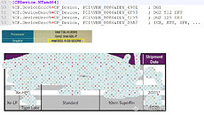
Source:
VideoCardz
A leaked OEM data-sheet referencing the DG2 also mentions a rather contemporary video memory setup, with 8 GB of GDDR6 memory. While the Iris Xe MAX is built on Intel's homebrew 10 nm SuperFin node, Intel announced that its Xe-HPG chips will use third-party foundries. With these specs, Intel potentially has a GPU to target competitive e-sports gaming (where the money is). Sponsorship of major e-sports clans could help with the popularity of Intel Graphics. With enough beans on the pole, Intel could finally invest in scaling up the architecture to even higher client graphics market segments. As for availability, VideoCardz predicts a launch roughly coinciding with that of Intel's "Tiger Lake-H" mobile processor series, possibly slated for mid-2021.

34 Comments on Intel DG2 Xe-HPG Features 512 Execution Units, 8 GB GDDR6
GPGPU: Blender (intel.com)
ZLUDA is a project that can make it possible, but Intel isn't involved:
ZLUDA: Drop-In Open-Source CUDA Support For Intel Xe / UHD Graphics - Phoronix
So it looks like it will once again be in the hands of the developers to use OneAPI instead of CUDA, and sucess where Open Cl failed. (Wich could be a good thing since OneAPI isn't exclusive to Intel.) The good news is that the CPU side of OneAPI is already used by a few popular render engines, so maybe there's hope.
www.techpowerup.com/gpu-specs/xe-arctic-sound.c3503
www.tweaktown.com/news/74491/intel-arctic-sound-gpu-42-tflops-monster-4x-faster-than-playstation-5/index.html
Big Xe is 96EU - 768:48:24.
Intel is using a 50% bigger iGPU configuration.
Raven Ridge - max 1300 Mhz
Picasso - max 1400 Mhz
Renoir- max 1750 Mhz
Cezanne - max 2100 Mhz