Jul 25th, 2025 07:56 CDT
change timezone
Latest GPU Drivers
New Forum Posts
- How to get free Windows 10 security updates through October 2026: Two ways (11)
- AI Job Losses: let's count the losses up, total losses to AI so far 94,000 and counting (66)
- Which Linux flavor? (58)
- R9 7900X - 5070Ti - Lags / Stuttering (31)
- What's your latest tech purchase? (24363)
- DTS DCH Driver for Realtek HDA [DTS:X APO4 + DTS Interactive] (2233)
- Questionable quality future game releases being considered (3)
- Sapphire ATI 4850x2 - messed up the flash.... (4)
- Lexar NM790 (4TB) made my PC go back to Windows XP days, since it caused my PC to be SO slow and laggy! (27)
- Kindly help me to complete my new PC build... (7)
Popular Reviews
- Noctua NF-A12x25 G2 PWM Fan Review
- MSI MPG B850I Edge Ti Wi-Fi Review
- UPERFECT UMax 24 Review
- Cougar OmnyX Review
- TerraMaster F4-424 Max Review - The fastest NAS we've tested so far
- VAXEE XE V2 Wireless Review
- Sharkoon OfficePal C10 Review - Affordable and Decent
- Thermal Grizzly WireView Pro Review
- Upcoming Hardware Launches 2025 (Updated May 2025)
- Razer Blade 16 (2025) Review - Thin, Light, Punchy, and Efficient
TPU on YouTube
Controversial News Posts
- Some Intel Nova Lake CPUs Rumored to Challenge AMD's 3D V-Cache in Desktop Gaming (140)
- AMD Radeon RX 9070 XT Gains 9% Performance at 1440p with Latest Driver, Beats RTX 5070 Ti (131)
- AMD's Upcoming UDNA / RDNA 5 GPU Could Feature 96 CUs and 384-bit Memory Bus (121)
- NVIDIA GeForce RTX 5080 SUPER Could Feature 24 GB Memory, Increased Power Limits (115)
- NVIDIA DLSS Transformer Cuts VRAM Usage by 20% (99)
- AMD Sampling Next-Gen Ryzen Desktop "Medusa Ridge," Sees Incremental IPC Upgrade, New cIOD (97)
- NVIDIA Becomes First Company Ever to Hit $4 Trillion Market-Cap (94)
- Windows 12 Delayed as Microsoft Prepares Windows 11 25H2 Update (92)
Monday, April 5th 2021

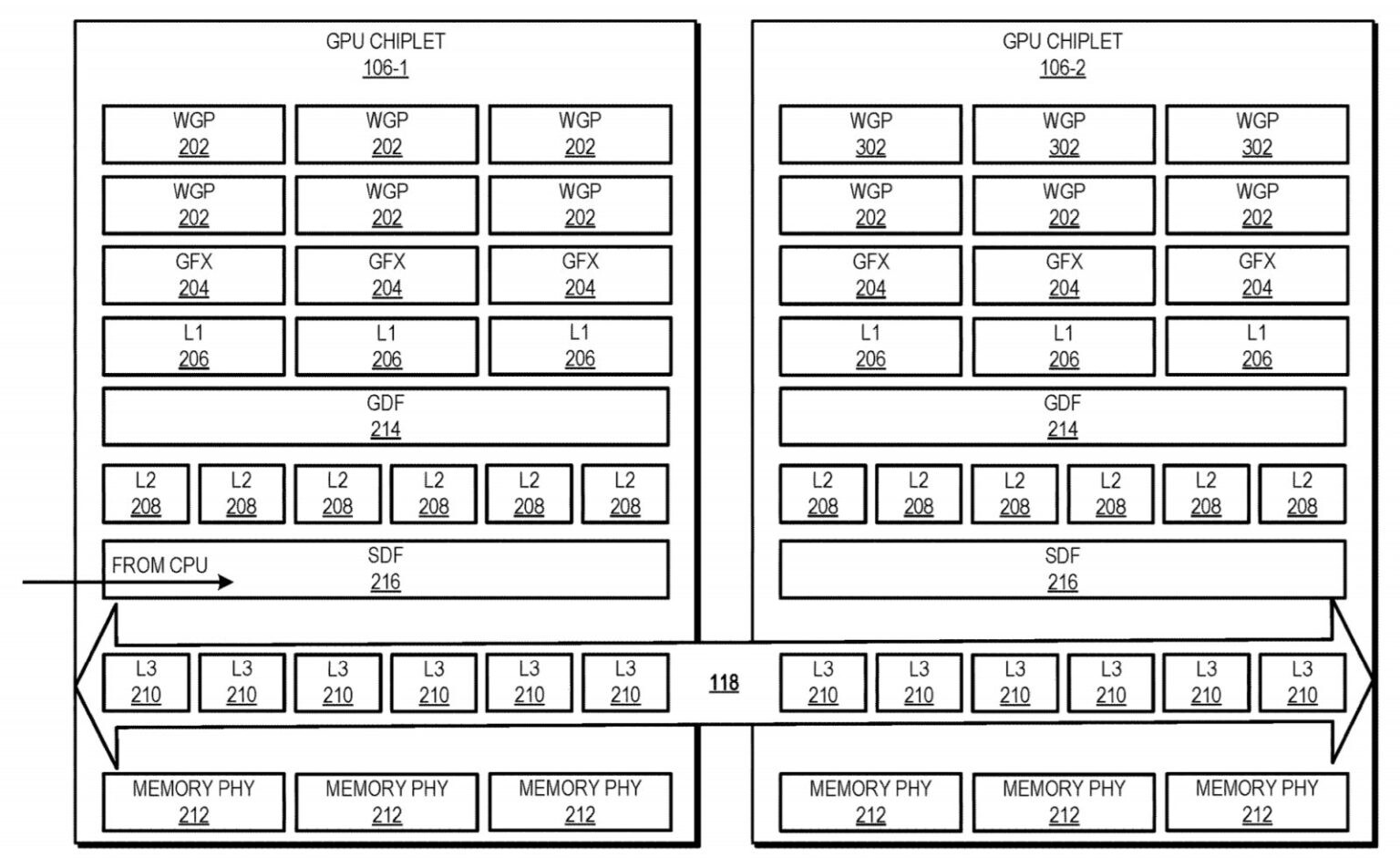
AMD Patents Chiplet-based GPU Design With Active Cache Bridge
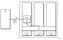
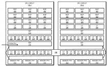
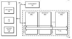
AMD on April 1st published a new patent application that seems to show the way its chiplet GPU design is moving towards. Before you say it, it's a patent application; there's no possibility for an April Fool's joke on this sort of move. The new patent develops on AMD's previous one, which only featured a passive bridge connecting the different GPU chiplets and their processing resources. If you want to read a slightly deeper dive of sorts on what chiplets are and why they are important for the future of graphics (and computing in general), look to this article here on TPU.
The new design interprets the active bridge connecting the chiplets as a last-level cache - think of it as L3, a unifying highway of data that is readily exposed to all the chiplets (in this patent, a three-chiplet design). It's essentially AMD's RDNA 2 Infinity Cache, though it's not only used as a cache here (and for good effect, if the Infinity Cache design on RDNA 2 and its performance uplift is anything to go by); it also serves as an active interconnect between the GPU chiplets that allow for the exchange and synchronization of information, whenever and however required. This also allows for the registry and cache to be exposed as a unified block for developers, abstracting them from having to program towards a system with a tri-way cache design. There are also of course yield benefits to be taken here, as there are with AMD's Zen chiplet designs, and the ability to scale up performance without any monolithic designs that are heavy in power requirements. The integrated, active cache bridge would also certainly help in reducing latency and maintaining chiplet processing coherency.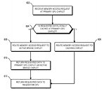
Sources:
Free Patents Online, via Videocardz
The new design interprets the active bridge connecting the chiplets as a last-level cache - think of it as L3, a unifying highway of data that is readily exposed to all the chiplets (in this patent, a three-chiplet design). It's essentially AMD's RDNA 2 Infinity Cache, though it's not only used as a cache here (and for good effect, if the Infinity Cache design on RDNA 2 and its performance uplift is anything to go by); it also serves as an active interconnect between the GPU chiplets that allow for the exchange and synchronization of information, whenever and however required. This also allows for the registry and cache to be exposed as a unified block for developers, abstracting them from having to program towards a system with a tri-way cache design. There are also of course yield benefits to be taken here, as there are with AMD's Zen chiplet designs, and the ability to scale up performance without any monolithic designs that are heavy in power requirements. The integrated, active cache bridge would also certainly help in reducing latency and maintaining chiplet processing coherency.


Jul 25th, 2025 07:56 CDT
change timezone
Latest GPU Drivers
New Forum Posts
- How to get free Windows 10 security updates through October 2026: Two ways (11)
- AI Job Losses: let's count the losses up, total losses to AI so far 94,000 and counting (66)
- Which Linux flavor? (58)
- R9 7900X - 5070Ti - Lags / Stuttering (31)
- What's your latest tech purchase? (24363)
- DTS DCH Driver for Realtek HDA [DTS:X APO4 + DTS Interactive] (2233)
- Questionable quality future game releases being considered (3)
- Sapphire ATI 4850x2 - messed up the flash.... (4)
- Lexar NM790 (4TB) made my PC go back to Windows XP days, since it caused my PC to be SO slow and laggy! (27)
- Kindly help me to complete my new PC build... (7)
Popular Reviews
- Noctua NF-A12x25 G2 PWM Fan Review
- MSI MPG B850I Edge Ti Wi-Fi Review
- UPERFECT UMax 24 Review
- Cougar OmnyX Review
- TerraMaster F4-424 Max Review - The fastest NAS we've tested so far
- VAXEE XE V2 Wireless Review
- Sharkoon OfficePal C10 Review - Affordable and Decent
- Thermal Grizzly WireView Pro Review
- Upcoming Hardware Launches 2025 (Updated May 2025)
- Razer Blade 16 (2025) Review - Thin, Light, Punchy, and Efficient
TPU on YouTube
Controversial News Posts
- Some Intel Nova Lake CPUs Rumored to Challenge AMD's 3D V-Cache in Desktop Gaming (140)
- AMD Radeon RX 9070 XT Gains 9% Performance at 1440p with Latest Driver, Beats RTX 5070 Ti (131)
- AMD's Upcoming UDNA / RDNA 5 GPU Could Feature 96 CUs and 384-bit Memory Bus (121)
- NVIDIA GeForce RTX 5080 SUPER Could Feature 24 GB Memory, Increased Power Limits (115)
- NVIDIA DLSS Transformer Cuts VRAM Usage by 20% (99)
- AMD Sampling Next-Gen Ryzen Desktop "Medusa Ridge," Sees Incremental IPC Upgrade, New cIOD (97)
- NVIDIA Becomes First Company Ever to Hit $4 Trillion Market-Cap (94)
- Windows 12 Delayed as Microsoft Prepares Windows 11 25H2 Update (92)
43 Comments on AMD Patents Chiplet-based GPU Design With Active Cache Bridge
-= edited=-
Remind me of hUMA, it all makes sense now why are they waiting to bring this to new AM5 platform with DDR5 RAM.
Infinitycache is Infinity Fabric for GPUs.
So rather than Infinity Fabric being a unified transport giving all CPU chiplets access to the memory controllers, Each GPU chiplet will have a baby/pseudo memory controller that seeds data into a massive shared L3 cache for all GPU chiplets too feed off.
Neat, probably. The move to chiplets will hurt overall IPC and efficiency slightly but it will move away from the single-biggest constraint GPUs have right now - manufacturing difficulties and yields on massive monolithic dies. You only have to look at the fact a 64C/128T Threadripper is available on a consumer/mainstream platform for the masses at $4000, whilst Intel is struggling so hard to get more than 24C in a processor that they'll charge $10-14K for the privilege and sell it only to server integrators as it's too much of a special snowflake to work in any non-proprietary mainstream platform using a regular, unified driver model.
AMD is shitting out 80mm² scalable chiplets at fantastic yields because of the small dies with 8C/16T and craploads of cache, whilst Intel's smallest 8C/16T part is 276mm² with zero scalability and half the cache.
Using the same silicon wafer yield calculator for both, AMD's gets ~696 sellable dies per wafer compared to Intel's ~161 sellable dies per wafer. Four times easier to make and the smaller die size also means that 92% of AMD's product is a flawless 8-core part, whilst around 25% of Intel's output needs to be harvested to make 6-core or worse.
So, if you take that example alone, GPU chiplets can't come soon enough.
I expect the patent trolls are already digging for that one line of code or whatever so they can sue.not like they can use the same name, that serves, essentially, the same function.
- Infinity Fabric connects cores to memory controllers, and cores manage their cache.
- Infinity cache connects cache to memory controllers, and cores manage their memory controllers.
I mean, sure - they both connect things which is the same function - but so do nails, tape, and string - yet those things are allowed to have different names? :pHere it is.
Sounds like RDNA 3 will be an interesting generation for sure!
Let say you modify some data. You will need to have the updated data available for other execution units. The easy way is to save it to ram, and them read it back but this add huge latency.
They use the L3 cache for that, this save a lot of time but when you have multiple L3 cache, you need to have mechanism that detect if the data is in another L3 cache and then collect it. (very simplified explanation)
Having it in the bridge is probably the best solution as it will be aware of all others chiplets. But, connecting that to each chiplets will add latency and will have reduced bandwidth. But chip design is all about compromise and making the best choice that give the best performance overall.
We will see
AMD had been successively expanding the chip resources, albeit never found the medium to express what it can do unequivocally.
How do you think it will affect 'Infinity Cache' sizes? This might mitigate 'all' outbound memory transfer needs of AMD.