News Posts matching #Infinity Cache

Return to Keyword Browsing

AMD Radeon RX 9050 4 GB Benchmarks Surface, 8 GB Model 37% Faster

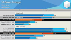
Hardware Unboxed and Toasty Bros have both tested the mysterious Radeon RX 9050 4 GB, and the results look rough. AMD only sells this version in OEM systems, so both channels had to buy CyberPowerPC prebuilts to get one. In Hardware Unboxed's 18-game test at 1080p Low, the 4 GB card averaged 78 FPS with 55 FPS 1% lows, against 107 FPS and 78 FPS for the RX 9050 8 GB. That makes the 8 GB model about 37% faster. At the lowest settings tested, it was still around 32% ahead, at 147 FPS versus 111 FPS. Both cards share 1,024 Stream Processors and up to a 2.6 GHz boost clock, so the difference comes from memory. As AMD confirmed, the 4 GB model has a 64-bit bus, 144 GB/s of bandwidth, and 16 MB of Infinity Cache, exactly half of what the 8 GB model has.

Toasty Bros opened their prebuilt and found an XFX dual-fan card with a single 8-pin connector, so it looks like ASRock is not the only partner making one. AMD has said it developed the Radeon RX 9050 4 GB version for a specific partner system aimed at entry-level gaming customers, and that it has no plans to sell it outside that OEM PC. The card was first spotted in a CyberPowerPC Gamer Master prebuilt at Best Buy, which was listed at $889.99. Keep in mind that this is still a small sample, with only two outlets testing the card so far, so it's important to wait for more independent results before drawing firm conclusions. Still, AMD launching a card with only 4 GB of VRAM in 2026 is not looking like a great decision so far.

AMD Confirms Radeon RX 9050 4 GB Has Smaller Infinity Cache, Lower Memory Bandwidth

AMD has updated its documentation page for the late-July launch of the Radeon RX 9050 graphics cards, which include two models: one with 4 GB and another with 8 GB of GDDR6 memory. Both cards feature 1,024 Streaming Processors across 16 Compute Units and can boost up to a 2.6 GHz clock speed. However, the lower-end GPU has only 4 GB of GDDR6 memory on a 64-bit bus, resulting in a memory bandwidth of 144 GB/s, which is significantly lower than the 8 GB version. The 8 GB version of the Radeon RX 9050 uses 8 GB of GDDR6 on a 128-bit bus, providing a memory bandwidth of 288 GB/s, doubling the throughput.

Another difference lies in the Infinity Cache within each GPU die. The 8 GB edition has 32 MB of Infinity Cache, while the 4 GB edition has only 16 MB. Initially, the listing for the 4 GB edition did not reveal the difference in Infinity Cache size, but AMD's documentation confirms it. Naturally, this will result in some performance differences, as larger cache buffers tend to improve performance significantly.

Sapphire Intros Radeon RX 9050 8GB Pulse Graphics Card

Sapphire today introduced its Radeon RX 9050 Pulse 8 GB graphics card. Based on a compacted variant of its RX 9060 XT Pulse board design, the card forms AMD's new entry-level in the RX 9000 series generation of GPUs powered by RDNA 4 graphics architecture. AMD carved the RX 9050 out of the 4 nm "Navi 44" silicon by enabling 16 out of 32 compute units physically present on the silicon, resulting in 1,024 stream processors. The SKU interestingly gets the entire 32 MB Infinity Cache present on the silicon. It also features the chip's full 128-bit wide GDDR6 memory bus, and this particular card features 8 GB of 18 Gbps GDDR6 memory.

Sapphire's board design for the RX 9050 Pulse 8 GB features a dense aluminium fin-stack heatsink featuring two 6 mm-thick copper heat pipes. The fin-stack is ventilated by a pair of 70 mm fans. The card takes in a single 8-pin PCIe power connection that's sufficient for its 100 W typical board power. Display outputs include two HDMI 2.1b and one DisplayPort 2.1a connectors. The card is 20 cm in length, 12.2 cm in height, and is strictly 2 slots thick. The company didn't reveal pricing.

AMD Launches Radeon RX 9070 GRE Worldwide at $550

AMD today announced a global launch of the Radeon RX 9070 GRE graphics card. The card was debuted as a China-exclusive, and is seeing a wider launch to fill a key price-performance gap that exists between the RX 9060 XT 16 GB and the RX 9070. The new RX 9070 GRE carved out from the same 4 nm "Navi 48" silicon as the RX 9070 and RX 9070 XT. While the silicon physically has 64 compute units and a 256-bit wide memory bus, the RX 9070 GRE is configured with three quarters of it, featuring 48 compute units, and a 192-bit memory bus. In comparison, the RX 9060 XT and the "Navi 44" silicon it's based on, has exactly half the CU count and memory bus width.

The Radeon RX 9070 GRE hence has 3,072 stream processors, 48 RT accelerators, 96 AI accelerators, 192 TMUs, and 96 ROPs. The card gets 12 GB of 18 Gbps GDDR6 memory across its 192-bit wide memory bus, for 437 GB/s of memory bandwidth. It's also configured with 48 MB of Infinity Cache memory, three quarters of the 64 MB physically present on "Navi 48." The card is configured with 2.20 GHz of Game clock, and 2.79 GHz of maximum boost frequency for the GPU engine clock domain, while the memory ticks at 18 Gbps (GDDR6-effective). The main competition for this card is NVIDIA's GeForce RTX 5060 Ti 16 GB, which is priced at $570. AMD, in its first-party performance tests claims a significant 22% performance gain over the RTX 5060 Ti 16 GB, and a 26% performance-price gain. While NVIDIA recommends the RTX 5060 Ti for 1080p gaming, AMD is confident in the RX 9070 GRE being a 1440p-class gaming GPU. The card will be available from today, June 1st, through AMD's various add-in board (AIB) partners, including Sapphire, PowerColor, ASRock, XFX, GIGABYTE, Acer, and ASUS.

AMD Plans to Release Radeon AI Pro R9700S and R9600D Graphics Cards

AMD is preparing two new professional GPUs: Radeon AI Pro R9700S and Radeon AI Pro R9600D, built off the Radeon AI Pro R9700 that launched on October 27. References to the R9600D recently appeared in AMD's 25.30.1 Linux driver, and reports suggest both cards are planned for announcement around CES 2026. The R9700S is described as a server-focused variant of the standard R9700. Instead of the blower cooler used on the original model, the R9700S is expected to switch to passive cooling for use in data-center systems that rely on chassis airflow. The R9600D is positioned as a cut-down version of the same GPU, similar in naming strategy to AMD's earlier Pro W7900D.

Since both cards are rumored to be based on the existing R9700, their general configuration should be similar. The R9700 uses a 4 nm Navi 48 GPU with 64 RDNA 4 compute units, totaling 4,096 stream processors and 128 AI accelerators. It ships with 32 GB of 20 Gbps GDDR6 on a 256-bit interface for 640 GB/s of bandwidth, backed by 64 MB of 3rd-generation Infinity Cache. AMD rates the card at up to 191 TFLOPS of FP16 dense compute or 1531 TOPS of INT4 performance, with a 300 W power target. The R9700 launched as a dual-slot, blower-style card designed for multi-GPU inference systems. The upcoming R9700S and R9600D would expand this lineup, offering a passive server option and a lower-tier configuration built from the same RDNA 4 foundation.

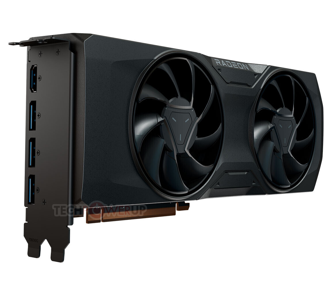
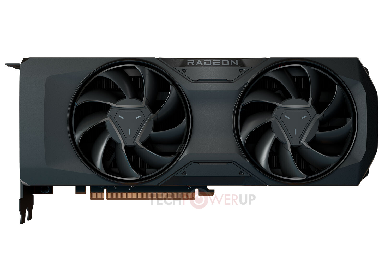
ASRock Launches Radeon RX 7700 Challenger Graphics Cards with 16 GB Memory

ASRock has unveiled its Radeon RX 7700 Challenger 16 GB graphics card, AMD's surprise new desktop gaming GPU that slots below the RX 7700 XT with a unique memory configuration targeting gamers seeking higher VRAM capacity for memory-intensive scenarios. The card features AMD's Navi 32 GPU with 2,560 cores, which is 26% fewer than the RX 7700 XT variant. However, AMD has equipped it with 16 GB of GDDR6 memory running at 19.5 Gbps on a 256-bit bus, compared to the XT's 12 GB at 18 Gbps. In this configuration we have 44% higher memory bandwidth despite the reduced core count.

ASRock's non-overclocked Challenger model reveals AMD's reference clock speeds: 2,041 MHz game clock and 2,459 MHz boost clock. The card includes 40 RDNA 3 Compute Units with RT and AI accelerators, plus 40 MB of AMD Infinity Cache technology. Power requirements include dual 8-pin connectors with a recommended 650 W PSU, though AMD hasn't disclosed the Total Board Power specification. Display connectivity includes three DisplayPort 2.1 and one HDMI 2.1 output over PCIe 4.0 interface. The Challenger maintains ASRock's established 2.5-slot dual-fan design with a metal backplate, striped ring fans, ultra-fit heatpipes, LED indicators, and 0dB silent cooling technology. Exact availability and pricing are yet unknown.

AMD's Next-Gen UDNA: Four Die Sizes, One Potential 96-CU Flagship

New block diagrams from a well-known hardware leaker @Kepler_L2 sketch out a very modular AMD UDNA family that could include four die sizes, with the largest rumored to reach 96 compute units. The images show repeating shader arrays and shader engines, each engine holding a handful of compute units and its own render backend. Those engines feed into a central SoC block that contains the graphics command processor, the graphics engine, hardware schedulers, and a shared L2 cache. On the memory side, the flagship diagram shows sixteen unified memory controllers, each with 32 bits, which would add up to a 512-bit external interface. The leak also mentions the possibility of a much larger on-die Infinity Cache for the top part.

If you map the parts together, the flagship's numbers line up with the diagram. Eight shader arrays with two shader engines each give 16 shader engines, and with six compute units per engine, that reaches the 96 CU figure. The mid-tier design pares things back: four shader arrays and eight shader engines, with five compute units per engine, which is about 40 compute units and an estimated six memory controllers for a 192-bit bus. Below that are 24 CU and 12 CU designs built from smaller arrays and fewer controllers. The 24 CU design is shown with as many as eight memory controllers, which could mean different controller widths depending on whether the part uses a traditional GDDR style interface or an LPDDR5X-like arrangement.

AMD Radeon RX 9070 GRE Tested, Fills Gap Between RX 9060 XT and RX 9070

AMD released the China-exclusive Radeon RX 9070 GRE in May, and ComputerBase.de caught hold of a Sapphire Pulse branded RX 9070 GRE card to test. While the RX 9060 XT specs sheet reads as being exactly half of the RX 9070 XT, the RX 9070 GRE is configured to be three quarters of it. It's based on the same 4 nm "Navi 48" silicon as the rest of the RX 9070 series, but is configured with 48 compute units out of the 64 present, and comes with 12 GB of memory across a 192-bit wide GDDR6 memory bus, in place of the 256-bit wide one that the RX 9070 and RX 9070 XT come with. With 48 CU, the RX 9070 GRE has 3,072 stream processors, 96 AI accelerators, 48 RT accelerators, 192 TMUs, and 96 ROPs. The Infinity Cache size is reduced to 48 MB. The card comes with the same 220 W TBP as the RX 9070.

Testing by ComputerBase.de finds that despite its reduction in compute units and memory, the RX 9070 GRE is still a 1440p-class GPU, and a significant upgrade over the RX 9060 XT 16 GB and the NVIDIA GeForce RTX 5060 Ti 16 GB. Averaged across 13 game tests, at 1440p, the RX 9070 GRE tests 28.4% faster than RX 9060 XT 16 GB, 22% faster than RTX 5060 Ti 16 GB, and 11% faster than the previous-gen RX 7800 XT, and 5% faster than RTX 4070. The current-gen RTX 5070 is 9% faster, RX 9070 is 14% faster, and the current flagship RX 9070 XT is 29% faster. This makes the RX 9070 GRE an interesting SKU that's at the intersection of various price-performance combinations within the 1440p class. In the Chinese domestic market, the RX 9070 GRE is priced slightly higher than the RTX 5060 Ti 16 GB, but lower than the RTX 5070, making it a good value proposition. Find more test results and insights in the source link below.

AMD Formally Launches Ryzen Threadripper PRO 9000 and Radeon AI PRO 9000 Series

AMD today formally launched a slew of new hardware for workstations. These include the new Ryzen Threadripper PRO 9000 "Shimada Peak" line of high core-count processors, and the Radeon AI PRO 9000 line of graphics cards that cover a range of use-cases spanning from edge AI acceleration to professional visualization. The Threadripper 9000 series is based on the "Zen 5" microarchitecture, and "Shimada Peak" is a variant of the "Turin" MCM powering 5th Gen EPYC processors, which comes with workstation-relevant I/O. Meanwhile, the Radeon AI Pro 9000 series is based on the same RDNA 4 graphics architecture powering the Radeon RX 9000 series gaming graphics cards.

The Ryzen Threadripper 9000 series comes with CPU core counts of up to 96-core/192-thread, with an IPC uplift from the "Zen 5" microarchitecture over the previous Threadripper 7000 series "Storm Peak" processors powered by "Zen 4." More than IPC, workstation users should benefit greatly from the architecture's full 512-bit FPU data-path, offering significant increases in performance of applications that leverage the AVX-512 instruction set. AMD also fine-tuned the IOD (I/O die) to support increased memory speeds of DDR5-6400 (native), AMD EXPO profiles, and CKD. With these changes, and minor increases in clock speeds for certain SKUs, AMD is promising a 16% uplift in performance over the Threadripper 7000 series predecessors in workstation benchmarks, and a significant 25% increase in SPEC Workstation AI and ML benchmarks (comparing identical core-counts and frequency).

AMD Instinct MI350X Series AI GPU Silicon Detailed

AMD today unveiled its Instinct MI350X series AI GPU. Based on the company's latest CDNA 4 compute architecture, the MI350X is designed to compete with NVIDIA B200 "Blackwell" AI GPU series, with the top-spec Instinct MI355X being compared by AMD to the B200 in its presentation. The chip debuts not just the CDNA 4 architecture, but also the latest ROCm 7 software stack, and hardware ecosystem based on the industry-standard Open Compute Project specification, which combines AMD EPYC Zen 5 CPUs, Instinct MI350 series GPUs, AMD-Pensando Pollara scale-out NICs supporting Ultra-Ethernet, and industry-standard racks and nodes, both in air- and liquid-cooled form-factors.

The MI350 is a gigantic chiplet-based AI GPU that consists of stacked silicon. There are two base tiles called I/O dies (IODs), each built on the 6 nm TSMC N6 process. This tile has microscopic wiring for up to four Accelerator Compute Die (XCD) tiles stacked on top, besides the 128-channel HBM3E memory controllers, 256 MB of Infinity Cache memory, the Infinity Fabric interfaces, and a PCI-Express 5.0 x16 root complex. The XCDs are built on the 3 nm TSMC N3P foundry node. These contain a 4 MB L2 cache, and four shader engines, each with 9 compute units. Each XCD hence has 36 CU, and each IOD seats 144 CU. Two IODs are joined at the hip by a 5.5 TB/s bidirectional interconnect that enables full cache coherency among the two IODs. The package has a total of 288 CU. Each IOD controls four HBM3E stacks for 144 GB of memory, the package has 288 GB.

SAPPHIRE Announces NITRO+ AMD Radeon RX 9070 Series Graphics Cards

SAPPHIRE Technology announces the latest SAPPHIRE NITRO+ AMD Radeon RX 9070 XT and Radeon RX 9070 graphics cards, built on the new AMD RDNA 4 architecture specialized for gamers and creators. With a plethora of new exciting features alongside the iconic powerful cooling engineering from the SAPPHIRE NITRO+ lineup, expect a new premium centerpiece for all gaming graphical needs.

NITRO Charged for an Elite Next Generation Adventure
The SAPPHIRE NITRO+ AMD Radeon RX 9070 Series Graphics Cards will be available in these enthusiast models:
  • SAPPHIRE NITRO+ AMD Radeon RX 9070 XT GPU with 16 GB memory, AMD RDNA 4 architecture, DisplayPort 2.1a
  • SAPPHIRE NITRO+ AMD Radeon RX 9070 GPU with 16 GB memory, AMD RDNA 4 architecture, DisplayPort 2.1a

AMD Introduces the Radeon PRO V710 to Microsoft Azure

AMD today introduced the Radeon PRO V710, the newest member of AMD's family of visual cloud GPUs. Available today in private preview on Microsoft Azure, the Radeon PRO V710 brings new capabilities to the public cloud. The AMD Radeon PRO V710's 54 Compute Units, along with 28 GB of VRAM, 448 GB/s memory transfer rate, and 54 MB of L3 AMD Infinity Cache technology, support small to medium ML inference workloads and small model training using open-source AMD ROCm software.

With support for hardware virtualization implemented in compliance with the PCI Express SR-IOV standard, instances based on the Radeon PRO V710 can provide robust isolation between multiple virtual machines running on the same physical GPU and between the host and guest environments. The efficient RDNA 3 architecture provides excellent performance per watt, enabling a single slot, passively cooled form factor compliant with the PCIe CEM spec.

AMD Intros Radeon RX 7800M Mobile Graphics Based on "Navi 32" Silicon

AMD officially launched the Radeon RX 7800M mobile graphics, which fills the rather vast gap that exists between its flagship Radeon RX 7900M, and the mid-range RX 7600M XT. This is the first official outing of the "Navi 32" GPU on the mobile platform. The RX 7800M maxes out the "Navi 32," enabling all 60 compute units, however, it does not max out the memory bus. The RX 7800M comes with 12 GB of 18 Gbps GDDR6 memory across a 192-bit wide memory bus. This means that only three out of four memory cache dies (MCDs) of the "Navi 32" are enabled, giving the chip 48 MB of Infinity Cache.

The RX 7800M essentially has the GCD core configuration of the desktop RX 7800 XT, but with the memory and cache configuration of the desktop RX 7700 XT. The 60 CU give it 3,840 stream processors, 120 AI accelerators, 60 ray accelerators, 240 TMUs, and 96 ROPs. The GPU comes with a Game Clocks frequency of 2145 MHz, while the memory ticks at 18 Gbps (432 GB/s memory bandwidth). AMD has given the RX 7800M a total graphics power (TGP) value of 180 W, which makes it fit for performance-segment gaming notebooks and mobile workstations. For reference, the RX 7900M comes with a TGP range of 180-200 W.

AMD RDNA 4 GPU Memory and Infinity Cache Configurations Surface

AMD's next generation RDNA 4 graphics architecture will see the company focus on the performance segment of the market. The company is rumored to not be making a successor to the enthusiast-segment "Navi 21" and "Navi 31" chips based on RDNA 4, and will instead focus on improving performance and efficiency in the most high-volume segments, just like the original RDNA-powered generation, the Radeon RX 5000 series. There are two chips in the new RDNA 4 generation that have hit the rumor mill, the "Navi 48" and the "Navi 44." The "Navi 48" is the faster of the two, powering the top SKUs in this generation, while the "Navi 44" is expected to be the mid-tier chip.

According to Kepler_L2, a reliable source with GPU leaks, and VideoCardz, which connected the tweet to the RDNA 4 generation, the top "Navi 48" silicon is expected to feature a 256-bit wide GDDR6 memory interface—so there's no upgrade to GDDR7. The top SKU based on this chip, the "Navi 48 XTX," will feature a memory speed of 20 Gbps, for 640 GB/s of memory bandwidth. The next-best SKU, codenamed "Navi 48 XT," will feature a slightly lower 18 Gbps memory speed at the same bus-width, for 576 GB/s of memory bandwidth. The "Navi 44" chip has a respectable 192-bit wide memory bus, and its top SKU will feature a 19 Gbps speed, for 456 GB/s of bandwidth on tap.

AMD "Strix Halo" Processor Boosts up to 5.35 GHz, Geekbenched

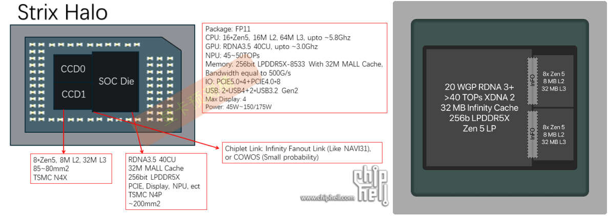
AMD's upcoming "Strix Halo" mobile processor that features up to 16 "Zen 5" CPU cores and a powerful iGPU with 40 compute units, is beginning to surface in online benchmark databases. We've gone into the juicy technical bits about the processor in our older articles, but put simply, it is a powerful mobile processor meant to square off against the likes of the Apple M3 Pro and M3 Max. A chiplet-based processor, much like the upcoming "Granite Ridge" desktop processor and "Fire Range" mobile processor, "Strix Halo" features up to 16 full-sized "Zen 5" cores, as it uses up to two of the same "Eldora" CCDs as them; but wired to a large I/O die that contains the oversized iGPU, and an NPU, besides the memory controllers. The iGPU has 40 compute units (2,560 stream processors), and is based on the RDNA 3.5 graphics architecture, while the NPU is the same 50 TOPS-class unit carried over from "Strix Point."

A prototype HP laptop powered by a "Strix Halo" processor that uses a single 8-core "Zen 5" CCD, was spied on the web. This chip has eight full-sized "Zen 5" cores that share a 32 MB L3 cache. The iGPU on the I/O die has its own 32 MB Infinity Cache memory that cushions memory transfers. In our older reports, we speculated as to what the memory interface of "Strix Halo" would be. It turns out that the chip exclusively features a 256-bit wide LPDDR5X memory interface, which is double the bus width of "Strix Point." This is essentially what a "quad-channel DDR5" memory interface would be, and AMD is using a memory speed standard of at least LPDDR5X-8000. From the machine's point of view, this would be just a couple of hardwired LPDDR5X chips, or a pair of LPCAMM 2 modules. Back to the benchmarks, and we are shown a single-thread CPU score of 2099 to 2177 points, and a multithreaded score ranging between 5477 points to 13993 points. The laptop was tested with an unknown version and distribution of Linux. The CPU cores are shown boosting up to 5.35 GHz.

AMD "Strix Halo" a Large Rectangular BGA Package the Size of an LGA1700 Processor

Apparently the AMD "Strix Halo" processor is real, and it's large. The chip is designed to square off against the likes of the Apple M3 Pro and M3 Max, in letting ultraportable notebooks have powerful graphics performance. A chiplet-based processor, not unlike the desktop socketed "Raphael," and mobile BGA "Dragon Range," the "Strix Halo" processor consists of one or two CCDs containing CPU cores, wired to a large die, that's technically the cIOD (client I/O die), but containing an oversized iGPU, and an NPU. The point behind "Strix Halo" is to eliminate the need for a performance-segment discrete GPU, and conserve its PCB footprint.

According to leaks by Harukaze5719, a reliable source with AMD leaks, "Strix Halo" comes in a BGA package dubbed FP11, measuring 37.5 mm x 45 mm, which is significantly larger than the 25 mm x 40 mm size of the FP8 BGA package that the regular "Strix Point," "Hawk Point," and "Phoenix" mobile processors are built on. It is larger in area than the 40 mm x 40 mm FL1 BGA package of "Dragon Range" and upcoming "Fire Range" gaming notebook processors. "Strix Halo" features one or two of the same 4 nm "Zen 5" CCDs featured on the "Granite Ridge" desktop and "Fire Range" mobile processors, but connected to a much larger I/O die, as we mentioned.

AMD RDNA 5 a "Clean Sheet" Graphics Architecture, RDNA 4 Merely Corrects a Bug Over RDNA 3

AMD's future RDNA 5 graphics architecture will bear a "clean sheet" design, and may probably not even have the RDNA branding, says WJM47196, a source of AMD leaks on ChipHell. Two generations ahead of the current RDNA 3 architecture powering the Radeon RX 7000 series discrete GPUs, RDNA 5 could see AMD reimagine the GPU and its key components, much in the same way RDNA did over the former "Vega" architecture, bringing in a significant performance/watt jump, which AMD could build upon with its successful RDNA 2 powered Radeon RX 6000 series.

Performance per Watt is the biggest metric on which a generation of GPUs can be assessed, and analysts believe that RDNA 3 missed the mark with generational gains in performance/watt despite the switch to the advanced 5 nm EUV process from the 7 nm DUV. AMD's decision to disaggregate the GPU, with some of its components being built on the older 6 nm node may have also impacted the performance/watt curve. The leaker also makes a sensational claim that "Navi 31" was originally supposed to feature 192 MB of Infinity Cache, which would have meant 32 MB segments of it per memory cache die (MCD). The company instead went with 16 MB per MCD, or just 96 MB per GPU, which only get reduced as AMD segmented the RX 7900 XT and RX 7900 GRE by disabling one or two MCDs.

ASRock Announces Radeon RX 7900 GRE Series Graphics Cards

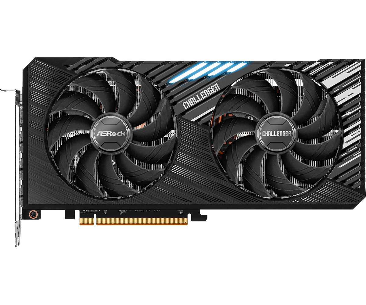
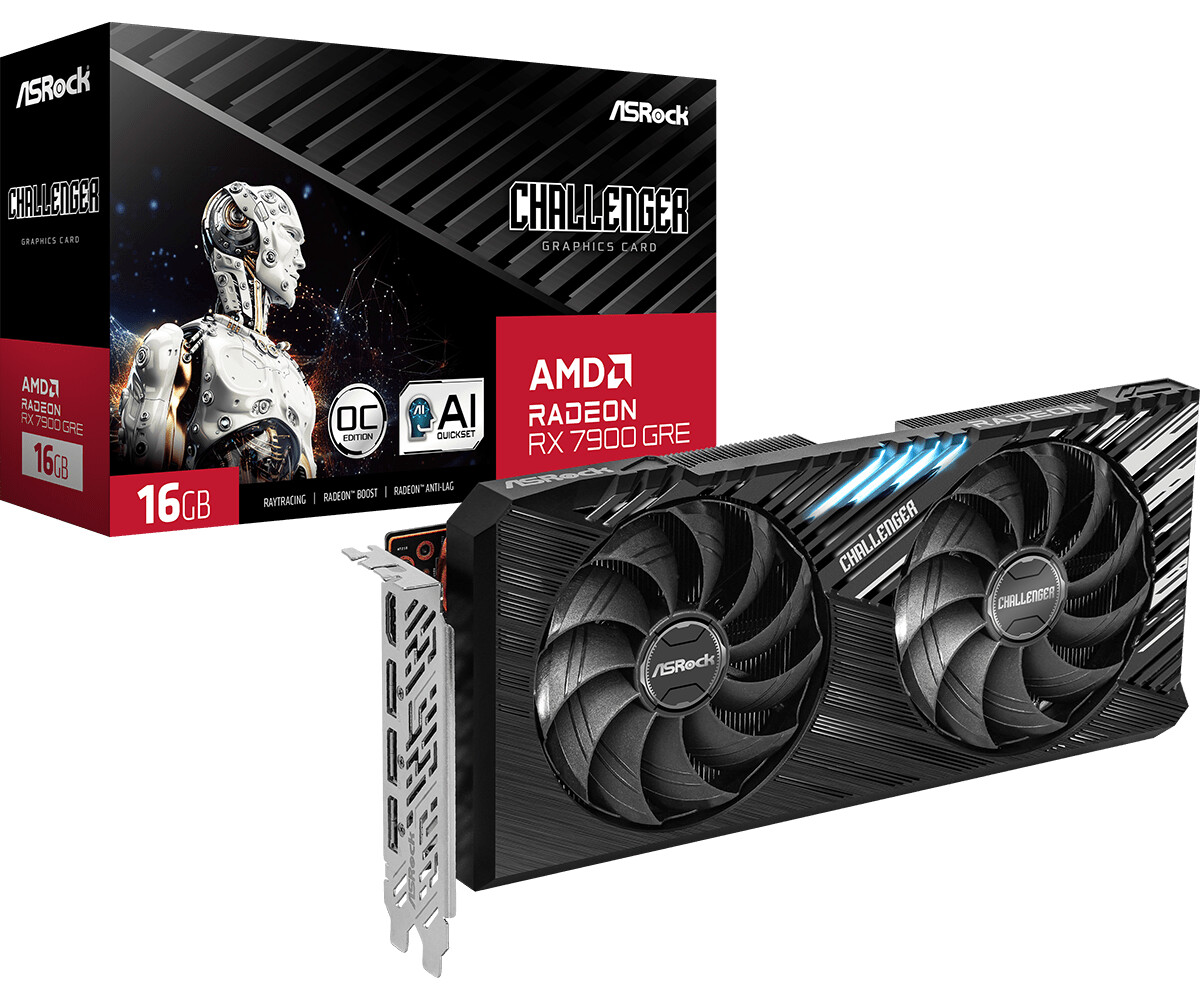
ASRock, the leading global motherboard, graphics card and mini PC manufacturer, today launched the new Steel Legend and Challenger series graphics cards based on the AMD Radeon RX 7900 GRE GPU. The new ASRock AMD Radeon RX 7900 GRE Series graphics cards are built on the groundbreaking AMD RDNA 3 architecture, featuring redesigned compute units, second-generation AMD Infinity Cache and ray tracing technologies, and increased AI throughput. They also feature the AMD Radiance Display Engine with support for DisplayPort 2.1, full AV1 encoding and are optimized for high-performance, high-resolution 4K/1440p gaming, streaming and content creation applications.

The new ASRock AMD Radeon RX 7900 GRE Series graphics cards are equipped with high-speed 16 GB GDDR6 memory at 18 Gbps, and are pre-overclocked to deliver higher levels of performance. In addition, the AMD Radiance Display Engine provides 12 bit-per-channel color for up to 68 billion colors for incredible color accuracy. ASRock AMD Radeon RX 7900 GRE Series graphics cards also support various ASRock exclusive features, including the Striped Ring/Axial Fan, Air Deflecting Fin, Ultra-fit Heatpipe, Metal Backplate, and Polychrome SYNC technology to provide great cooling efficiency, solid construction and fancy ARGB lighting effects. With these exclusive features, ASRock AMD Radeon RX 7900 GRE Series graphics cards are premium choices for 4K/2K gamers and creators.

AMD Radeon RX 7900 XT Drops to $710 on Newegg, MSRP Lowered to $749

AMD has lowered the official MSRP of the Radeon RX 7900 XT graphics card to $749, down from its launch price of $899. Its street price, as TweakTown found out, is lower still, with certain custom-design RX 7900 XT cards selling for as low as $710 on Newegg. At this price, the RX 7900 XT is set up for a major clash with certain overclocked NVIDIA GeForce RTX 4070 SUPER graphics cards, leftover inventories of the recently retired GeForce RTX 4070 Ti, and probably even looks to soak up some sales before the RTX 4070 Ti SUPER hits the scene on January 24. The cheapest RX 7900 XT is actually one of the better-appointed custom designs out there, the ASRock RX 7900 XT Phantom Gaming and XFX RX 7900 XT Merc 319, which had originally launched at prices comparable to the PowerColor Hellhound. These are followed by the PowerColor RX 7900 XT Hellhound and Sapphire RX 7900 XT Pulse OC at $720.

The Radeon RX 7900 XT is a very capable high-end GPU that AMD categorizes as capable of 4K Ultra HD gaming with settings maxed out. It's carved out from the "Navi 31" chiplet GPU, and configured with 84 RDNA3 compute units, worth 5,376 stream processors, 168 AI accelerators, 84 Ray accelerators, 336 TMUs, and 192 ROPs. The best part about this card is its memory sub-system, with 80 MB of Infinity Cache, and 20 GB of 20 Gbps GDDR6 memory across a 320-bit wide memory bus with 800 GB/s of bandwidth on tap, which should come in handy at 4K, or when using creator or AI applications.

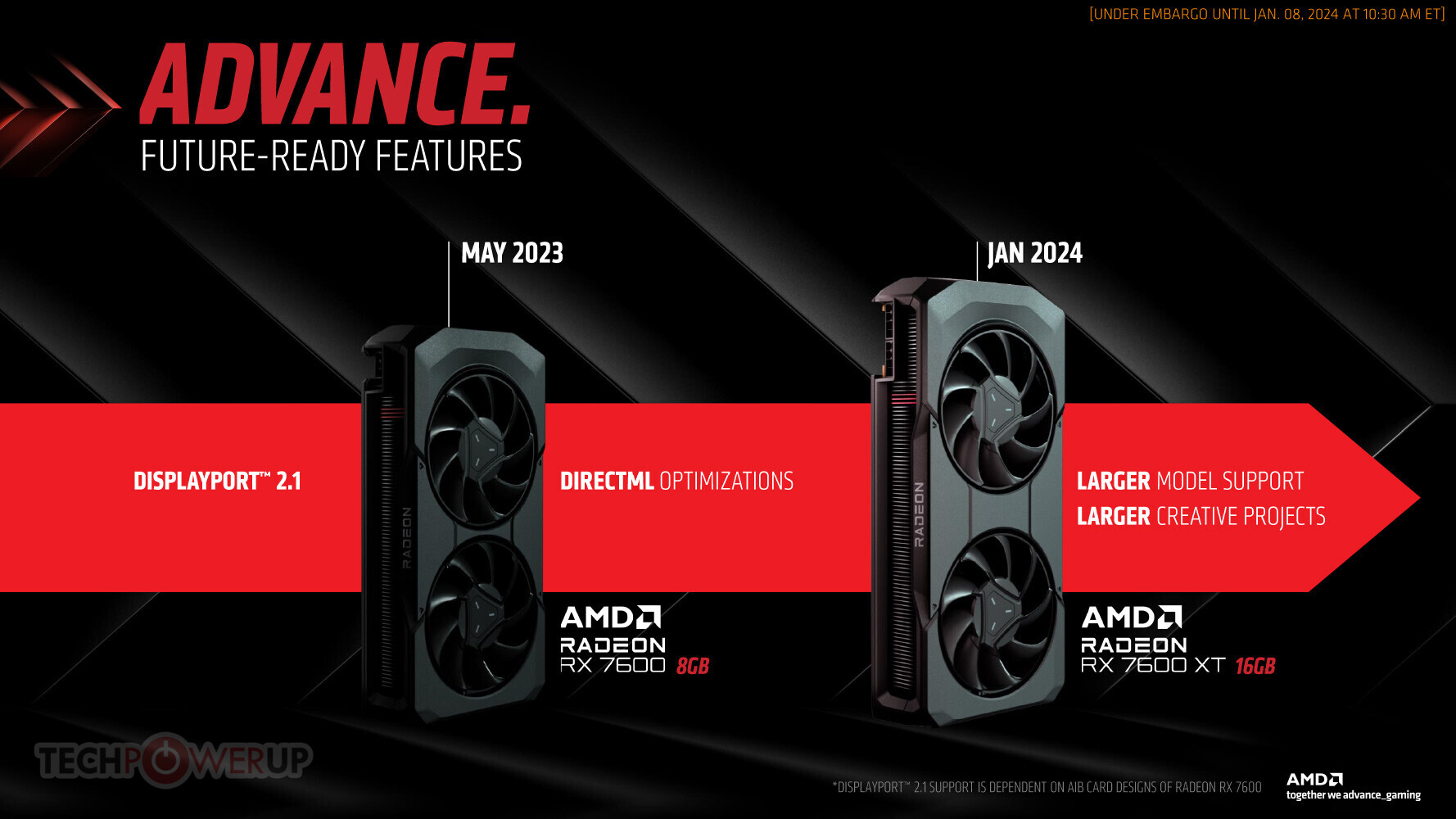
AMD Announces the Radeon RX 7600 XT 16GB Graphics Card

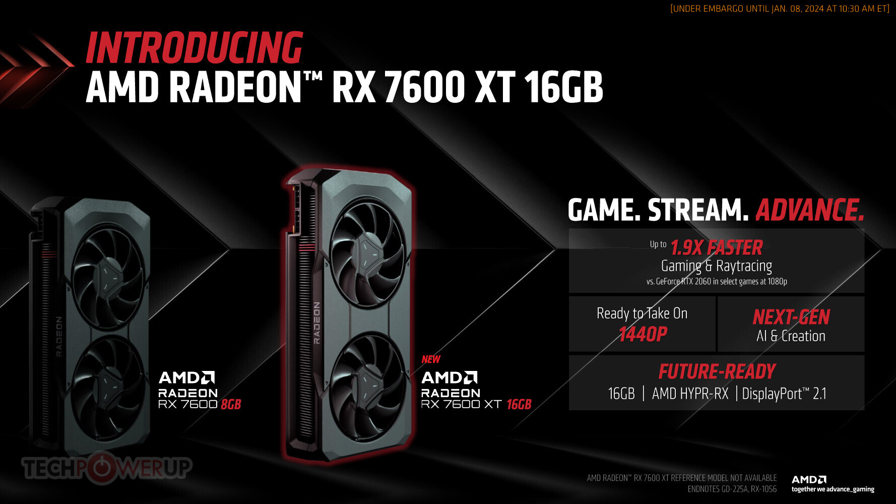
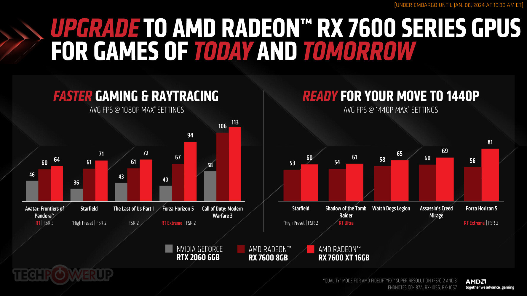
AMD announced the new Radeon RX 7600 XT graphics card, bolstering its mid-range of 1080p class GPUs. The RX 7600 XT is designed for maxed out AAA gaming at 1080p, although it is very much possibly to play many of the titles at 1440p with fairly high settings. You can also take advantage of technologies such as FSR 3 frame generation in games that support it, AMD Fluid Motion Frames on nearly all DirectX 12 and DirectX 11 games; as well as the new expanded AMD HyperRX performance enhancement that engages a host of AMD innovations such as Radeon Super Resolution, Anti-Lag, and Radeon Boost, to achieve a target frame rate.

The Radeon RX 7600 XT is based on the same 6 nm "Navi 33" silicon, and the latest RDNA 3 graphics architecture, as the Radeon RX 7600. If you recall, the RX 7600 had maxed out all 32 CU on the silicon. To design the RX 7600 XT, AMD retained the "Navi 33," but doubled the memory size to 16 GB, and increased the clock speeds. The 16 GB of memory is deployed across the same 128-bit wide memory bus as the 8 GB is on the RX 7600. The memory speed is unchanged, too, at 18 Gbps GDDR6-effective; as is the resulting memory bandwidth, of 288 GB/s. There are two key changes—the GPU clock speeds and power limits.

ASUS Intros China-exclusive Radeon RX 7900 GRE TUF White

ASUS over the weekend introduced the China-exclusive Radeon RX 7900 GRE TUF Gaming White graphics card. The card shares a lot in common with the other RX 7900 series TUF Gaming custom-design cards, but swaps out the gunmetal-gray cooler shroud and backplate combo for one that's matte white. The whitewash even extends to the impellers of the three Axial Tech fans. The PCB remains black, but due to the 3-D design of the shroud and backplate, is largely concealed. The card draws power from a pair of 8-pin PCIe power connectors, and uses a 14-phase VRM to condition it for the "Navi 31 XL" ASIC.

The Radeon RX 7900 GRE (golden rabbit edition) is based on a "Navi 31 XL," a unique package that combines the 5 nm graphics compute die (GCD) of "Navi 31," with the 4-MCD (memory cache die) setup of the smaller "Navi 32" package. AMD designed this primarily to drive the mobile RX 7900 series SKUs, but it found its way to the desktop platform to fill the gap between the RX 7800 XT and RX 7900 XT, and possibly undercut the GeForce RTX 4070 Ti. It is configured with 80 out of 96 available compute units on the GCD, giving it 5,120 stream processors, 160 AI accelerators, and 80 Ray accelerators, the Infinity Cache size is reduced to 64 MB, since there are only 4 MCDs, driving its 256-bit memory bus that handles 16 GB of 18 Gbps GDDR6 memory (576 GB/s bandwidth).

AMD Unveils Radeon RX 7800 XT and RX 7700 XT Graphics Cards

AMD today at Gamescom unveiled the Radeon RX 7800 XT and Radeon RX 7700 XT performance-segment graphics cards. Designed for maxed out gaming at 1440p with ray tracing, the two are designed to square off against NVIDIA's GeForce RTX 4070 series, offering competitive performance and pricing. The two are based on AMD's latest RDNA3 graphics architecture, and use the 5 nm foundry process where it matters. Both cards claim to offer not just superior performance to the specific NVIDIA RTX 40-series SKUs they're designed to compete with, but also better future-proofing, with more video memory on offer.

At the heart of the two is the new "Navi 32" GPU, AMD's second largest chip from this generation. It is a chiplet GPU, just like the "Navi 31" that powers the RX 7900 series, albeit slightly scaled down. The graphics compute die (GCD), the die with the main graphics rendering and compute machinery, is built on the 5 nm EUV foundry node. It is flanked by four memory cache dies (MCDs), each built on the 6 nm foundry node. These are the same MCDs found in the "Navi 31," but four in number instead of six, which gives the "Navi 32" a 256-bit wide GDDR6 memory interface.

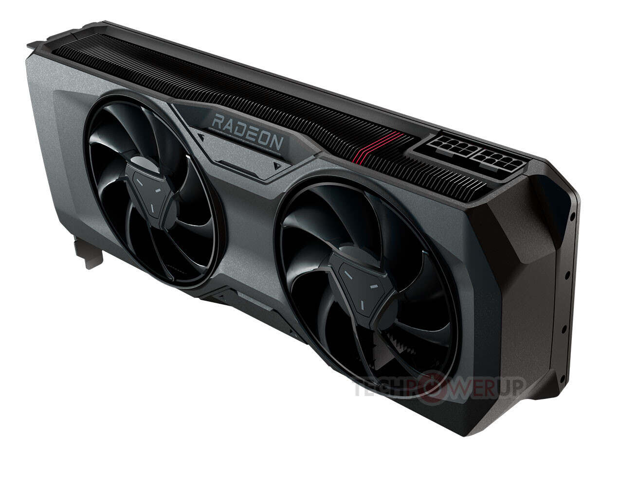
AMD Radeon RX 7800 XT and RX 7700 XT Reference Design Pictured

AMD, in a now-deleted tweet, revealed what it is probably going to announce later today—the Radeon RX 7800 XT and RX 7700 XT desktop graphics cards. The company briefly tweeted the marketing flier for these cards, before deleting it, but not before VideoCardz saved a copy. This flier confirms the SKU names RX 7800 XT and RX 7700 XT up for launch; and gives us two images of the Made by AMD (reference design) graphics card. It appears like AMD is using a common board design for both SKUs.

The reference Radeon RX 7800 XT appears to be a slightly shrunk down version of the RX 7900 XT reference. The dual-slot card comes with two axial-flow fans instead of three on the RX 7900 XT. The card draws power from two 8-pin PCIe power connectors. Earlier this month, a leak by PowerColor spilled the beans on the RX 7800 XT being based on the "Navi 32" silicon. A chiplet-based GPU just like the "Navi 31" powering the RX 7900 series; the Navi 32 is maxed out by the RX 7800 XT, and packs 3,840 stream processors, 120 AI accelerators, 60 Ray accelerators, 64 MB of Infinity Cache memory, and a 256-bit GDDR6 memory interface, which holds 16 GB of memory on the RX 7800 XT. Specs of the RX 7700 XT remain under the wraps.

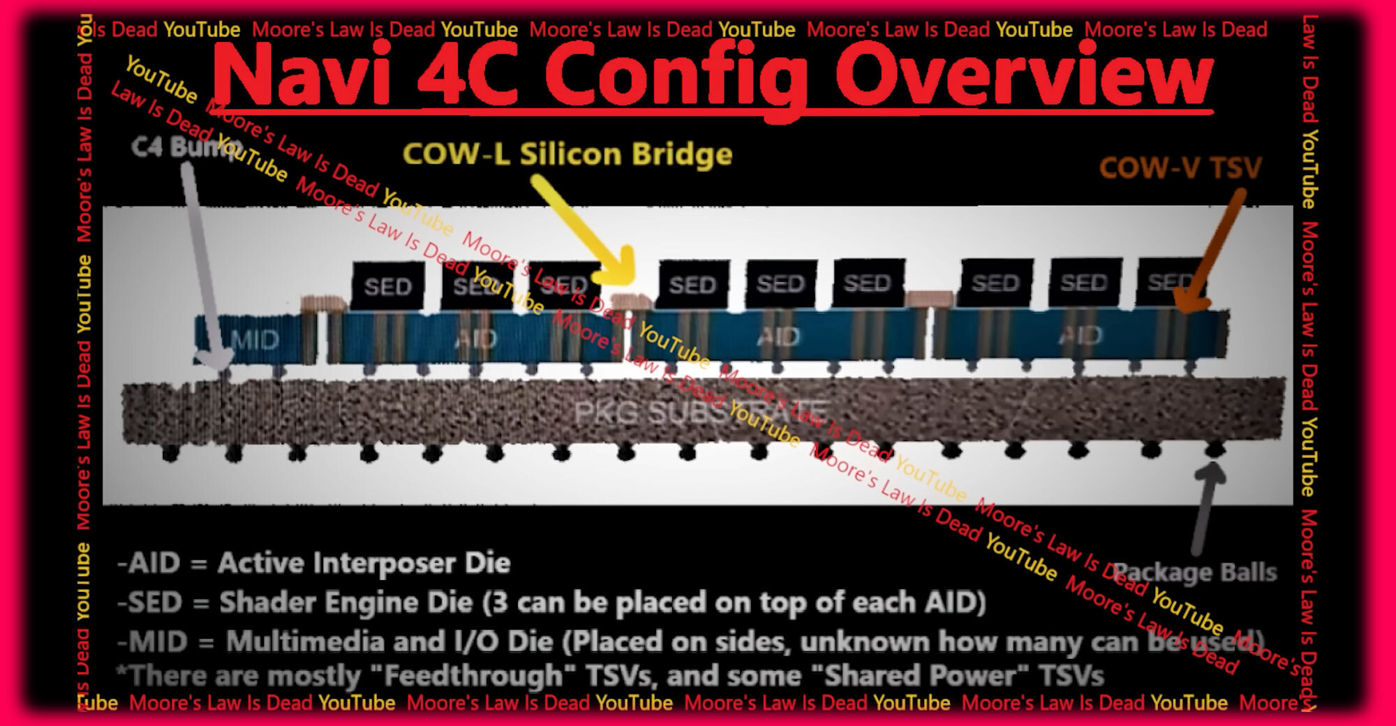
AMD "Navi 4C" GPU Detailed: Shader Engines are their own Chiplets

"Navi 4C" is a future high-end GPU from AMD that will likely not see the light of day, as the company is pivoting away from the high-end GPU segment with its next RDNA4 generation. For AMD to continue investing in the development of this GPU, the gaming graphics card segment should have posted better sales, especially in the high-end, which it didn't. Moore's Law is Dead scored details of what could have been a fascinating technological endeavor for AMD, in building a highly disaggregated GPU.

AMD's current "Navi 31" GPU sees a disaggregation of the main logic components of the GPU that benefit from the latest 5 nm foundry node to be located in a central Graphics Compute Die; surrounded by up to six little chiplets built on the older 6 nm foundry node, which contain segments of the GPU's Infinity Cache memory, and its memory interface—hence the name memory cache die. With "Navi 4C," AMD had intended to further disaggregate the GPU, identifying even more components on the GCD that can be spun out into chiplets; as well as breaking up the shader engines themselves into smaller self-contained chiplets (smaller dies == greater yields and lower foundry costs).

PowerColor AMD Radeon RX 7800 XT Pictured, Confirmed Based on "Navi 32"

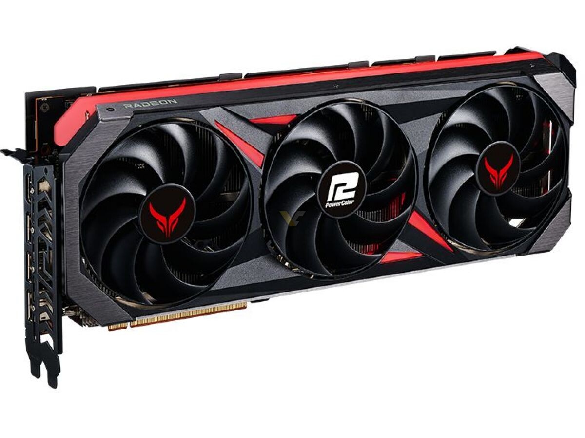
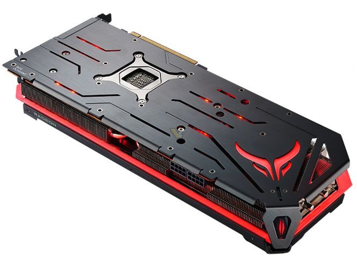
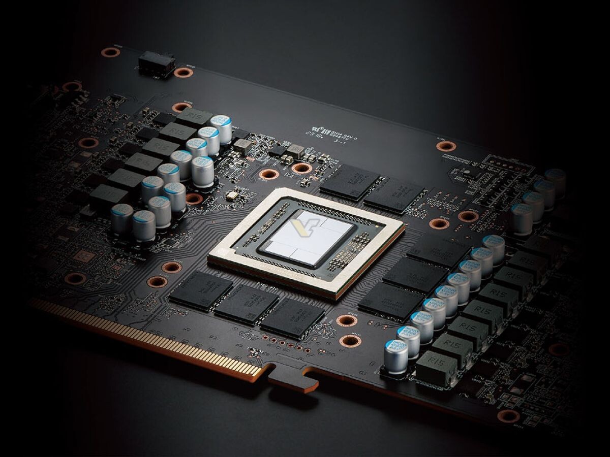
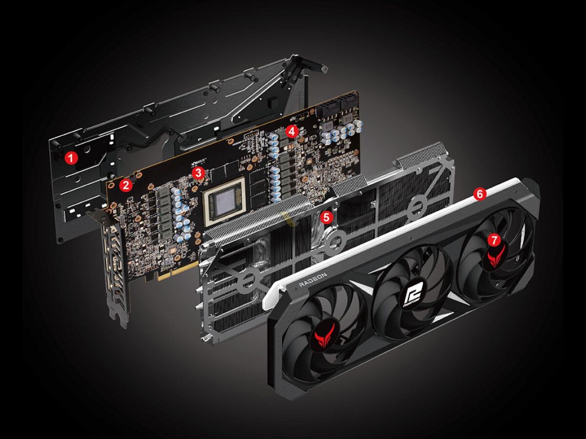
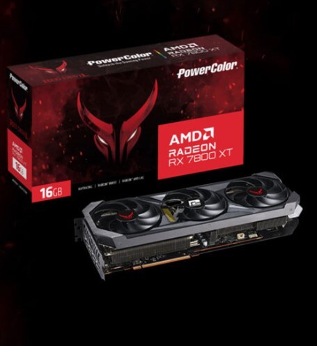
PowerColor inadvertently released the first pictures of its AMD Radeon RX 7800 XT Red Devil graphics card. These pictures confirm that the RX 7800 XT is based on a maxed out version of the "Navi 32" GPU, and not the compact "Navi 31" powering the limited edition RX 7900 GRE. The "Navi 32" is a chiplet-based GPU, just like the "Navi 31," albeit smaller. Its 5 nm GCD (graphics compute die) physically features 60 RDNA3 compute units, which work out to 3,840 stream processors, 120 AI accelerators, 60 Ray accelerators, 192 TMUs, and possibly 128 ROPs. This GCD is surrounded by four 6 nm MCDs (memory cache dies), which each has a 16 MB segment of the GPU's 64 MB Infinity Cache memory, and make up its 256-bit GDDR6 memory interface.

The specs sheet put out by PowerColor confirms that the RX 7800 XT maxes out the "Navi 32," enabling all 60 CUs, and the chip's full 256-bit memory interface, to drive 16 GB of memory. The RX 7800 XT uses 18 Gbps memory speed, and hence has 576 GB/s of memory bandwidth at its disposal. The PowerColor RX 7800 XT Red Devil has dual-BIOS, and assuming the "standard/silent" BIOS runs the card at AMD reference clock speeds, we're looking at Game clocks of 2210 MHz, and 2565 MHz boost. The Red Devil draws power from a dual 8-pin PCIe power connector set up (375 W max); the cooler is visibly smaller than the one on the company's RX 7900 series Red Devil cards. A 16+2 phase VRM powers the card. With pictures of the card out, we expect a global product launch within the next 30 days.
Return to Keyword Browsing
Nov 11th, 2026 03:16 CST change timezone

New Forum Posts

Popular Reviews

TPU on YouTube

Controversial News Posts