Monday, April 5th 2021

AMD Patents Chiplet-based GPU Design With Active Cache Bridge

AMD on April 1st published a new patent application that seems to show the way its chiplet GPU design is moving towards. Before you say it, it's a patent application; there's no possibility for an April Fool's joke on this sort of move. The new patent develops on AMD's previous one, which only featured a passive bridge connecting the different GPU chiplets and their processing resources. If you want to read a slightly deeper dive of sorts on what chiplets are and why they are important for the future of graphics (and computing in general), look to this article here on TPU.

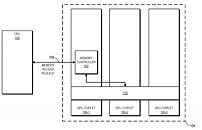
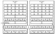
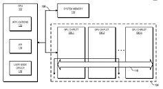
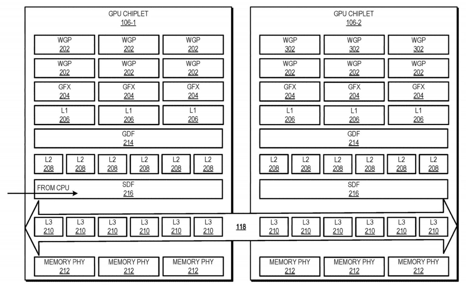
The new design interprets the active bridge connecting the chiplets as a last-level cache - think of it as L3, a unifying highway of data that is readily exposed to all the chiplets (in this patent, a three-chiplet design). It's essentially AMD's RDNA 2 Infinity Cache, though it's not only used as a cache here (and for good effect, if the Infinity Cache design on RDNA 2 and its performance uplift is anything to go by); it also serves as an active interconnect between the GPU chiplets that allow for the exchange and synchronization of information, whenever and however required. This also allows for the registry and cache to be exposed as a unified block for developers, abstracting them from having to program towards a system with a tri-way cache design. There are also of course yield benefits to be taken here, as there are with AMD's Zen chiplet designs, and the ability to scale up performance without any monolithic designs that are heavy in power requirements. The integrated, active cache bridge would also certainly help in reducing latency and maintaining chiplet processing coherency.
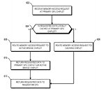
AMD Chiplet Design Patent with Active Cache Hierarchy AMD Chiplet Design Patent with Active Cache Hierarchy AMD Chiplet Design Patent with Active Cache Hierarchy AMD Chiplet Design Patent with Active Cache Hierarchy
Sources: Free Patents Online, via Videocardz
Add your own comment

43 Comments on AMD Patents Chiplet-based GPU Design With Active Cache Bridge

#26
evernessince
TheoneandonlyMrKWhile I agree with most of your points, I so think your wrong on efficiency and IPC because people (Not AMD but scientists I can't recall including those of Nvidia)have already proven that it can be both more efficient and give higher IPC, forget people even, AMD themselves also proved it with the Zen architecture
Correct. This is what you are referring to in particular: www.cs.ucy.ac.cy/conferences/pact2018/material/PACT2008-public.pdf
Posted on Reply
#27
Steevo
The biggest gains will be in clock speed, multiple domains for multiple chiplets and each can be engineered for IPC, clock speed, and or latency as required.

Imagine 4 chiplets with 4Ghz boost speeds, a 2Ghz cache that is massively parallel with compression technology, a couple tiny chiplets for video encode/decode and for low power applications.

Now add on the stacked die tech that has been learned to create a parallel pipeline for pure vector math for Ray tracing stacked on each of the main 4 chiplets that can read and write to caches on the primary die. Ray tracing with the only performance penalty being extra heat and a fraction of the latency.
Posted on Reply
#29
Minus Infinity
Possibly a glimpse of RDNA4's future, doubt we'll see this in RDNA3. Mostly likely will go up against Hopper which was delayed and replaced by Lovelace for next gen.
Posted on Reply
#30
evernessince
mtcn77Doesn't it say MCM adds as much as +1GHz!
Correct. By separating the CPU cores into a separate die you gain the ability to further bin which CPU die ends up on which CPU. This is how AMD is able to have it's 16 core 5950X that consumes less power than it's 12 core while also using less power. The 5950X is about 28% more power efficient than other Ryzen 5000 series CPUs through binning alone. AMD likely decided to go for efficiency instead of extra clocks for two reasons 1) Intel doesn't have anything competitive to it's 12 and 16 core mainstream CPUs 2) The power consumption goes up much faster above the sweet spot. Increasing the GHz would improve ST performance but at a cost. AMD likely calculated that given Intel's current prospects, it would be better to focus on efficiency.
Posted on Reply
#31
ltkAlpha
PunkenjoyThis is mostly true altought less and less true as there are more and more technique that reuse generated data. This is also why SLI/Crossfire is dead. The latency to move these data was just way too big. Temporal AA, ScreenSpace reflection, etc...
Can't you have one chiplet dealing with frame/scene level calculations after you've powered through the more easily parallelizable tasks? As in 1 Bigger (perhaps on the hub chip to reduce latency to the cache) + N Small(er)?
Posted on Reply
#32
mtcn77
evernessinceIncreasing the GHz would improve ST performance but at a cost.
You approach from a cpu stand point. On a gpu, the ST isn't the only factor, internal bandwidth is a major proponent. The bandwidth is a lot on a gpu however bandwidth per CU needs a lot of use to leverage fully, since the memory unit is external to the chip. Running it faster solves that problem.
Bets: 3.5GHz gpus over the horizon, or not?
Posted on Reply
#33
evernessince
mtcn77You approach from a cpu stand point. On a gpu, the ST isn't the only factor, internal bandwidth is a major proponent. The bandwidth is a lot on a gpu however bandwidth per CU needs a lot of use to leverage fully, since the memory unit is external to the chip. Running it faster solves that problem.
Bets: 3.5GHz gpus over the horizon, or not?
I'd say it's equally as possible that we see MCM GPU architectures that simply target the frequency sweetspot and spend any extra power budget add more cores, cache, ect. It really depends though, for all we know AMD or Nvidia could design their GPU chiplets to clock very high and thus the sweetspot would follow suite. I'm not knowledgeable enough on the topic to say to the extent that Nvidia / AMD and TSMC can influence ideal GPU clockspeed based on design / node.
Posted on Reply
#34
mtcn77
evernessinceI'd say it's equally as possible that we see MCM GPU architectures that simply target the frequency sweetspot and spend any extra power budget add more cores, cache, ect. It really depends though, for all we know AMD or Nvidia could design their GPU chiplets to clock very high and thus the sweetspot would follow suite. I'm not knowledgeable enough on the topic to say to the extent that Nvidia / AMD and TSMC can influence ideal GPU clockspeed based on design / node.
Me neither, although some would consider me an old timer.
Gpus, do associate with high frequency because the power cost is already paid for. Remember Hawaii series? AMD never integrated tiled 'buffered' rasterization up until Vega and thus the memory interface never slowed down since it was always running in immediate mode whereas Nvidia can keep tabs at various memory clocks.
It could improve utilization if the shaders request at a higher rate - gpus are throughput oriented, after all...
Posted on Reply
#35
Vya Domus
SteevoImagine 4 chiplets with 4Ghz boost speeds
There is going to be a long time before we'll see that if ever. Every kind of chip seems to start scaling horribly past the 3 Ghz mark, a GPU in particular will be horrendous efficiency wise at those kinds of speeds.
Posted on Reply
#36
HenrySomeone
AranarthSo for those of you waiting for AMD to do to nVidia what they did to Intel....

Here it is.

Sounds like RDNA 3 will be an interesting generation for sure!
What they did to Intel? You mean, as soon as they got competitive, they also became both more expensive and hard to get in the first place - what a fantastic prospect for the already beleaguered graphics cards market indeed!
Posted on Reply
#37
Aranarth
HenrySomeoneWhat they did to Intel? You mean, as soon as they got competitive, they also became both more expensive and hard to get in the first place - what a fantastic prospect for the already beleaguered graphics cards market indeed!
You DO realize that this is market forces at work right?

Demand outstripped supply so far that even though TSMC is running FLAT OUT they still cannot keep up!
They now spending 100 BILLION DOLLATRS over the next three years to build more plants so they can deal with the demand.

Then you have people buying them by the millisecond so fast with their bots that you cannot buy them through normal channels making a bad situation even worse.
But hey they do it because they can make 25 to 50% profit selling on ebay and through the gray market.

AMD made the decision to focus on supplying computer manufacturers and not direct sellers like newegg and amazon.
I just got a 6800xt and 5600x from Dell.
Placed my order, waited a month and here it is! AND I got both for what appears to be MSRP or close to it.


Be sure you are looking at the BIG PICTURE before lambasting people and companies for things that are out of their control.
Posted on Reply
#38
mtcn77
Vya DomusEvery kind of chip seems to start scaling horribly past the 3 Ghz mark, a GPU in particular will be horrendous efficiency wise at those kinds of speeds.
This could bring a split multiplier to run internal caches faster than the gpu. Don't dismiss it, the scaling isn't linear because memory is external and not helpful in the gpu pipeline flow directly - gpu speed, however, is. Nothing outside of cache speed changes that(maybe texture caching, too).
Posted on Reply
#39
Vya Domus
mtcn77This could bring a split multiplier to run internal caches faster than the gpu. Don't dismiss it, the scaling isn't linear because memory is external and not helpful in the gpu pipeline flow directly - gpu speed, however, is. Nothing outside of cache speed changes that(maybe texture caching, too).
Caches are power hogs, very high energy density per area, for that reason they usually run slower than the processor itself. The only portions of memory that run as fast the processor are the registers, everything else, including L1 caches typically run slower.
Posted on Reply
#40
mtcn77
Vya DomusCaches are power hogs, very high energy density per area, for that reason they usually run slower than the processor itself. The only portions of memory that run as fast the processor are the registers, everything else, including L1 caches typically run slower.
Well, guess what consumes power at an even higher rate than the caches - memory devices. The futility with saving power by cutting the effective rate is self explanatory. There is a way that is uses buffering to reduce accesses to memory and texture caching to supplant memory by sram. It ties with actual data flow across the die whereas the memory devices don't solve any bottlenecks, they are last level.
I'm not well versed enough, but there is no free lunch. SRAM offers much more than its substitutes.
Posted on Reply
#41
Vya Domus
mtcn77Well, guess what consumes power at an even higher rate than the caches - memory devices. The futility with saving power by cutting the effective rate is self explanatory. There is a way that is uses buffering to reduce accesses to memory and texture caching to supplant memory by sram. It ties with actual data flow across the die whereas the memory devices don't solve any bottlenecks, they are last level.
I'm not well versed enough, but there is no free lunch. SRAM offers much more than its substitutes.
Yes access to global memory is very inefficient power wise and cache hits improves that. But the problem is caches live on die and need to be cooled and eat away at the power budget of the chip.


Remember how the Infinity cache is placed around the CUs and not between them as to how you'd expect it to be ? I think it was a deliberate choice to place this huge chunk of cache on the extremities of the chip to reduce heat spots.
Posted on Reply
#42
Unregistered
AranarthSo for those of you waiting for AMD to do to nVidia what they did to Intel....

Here it is.

Sounds like RDNA 3 will be an interesting generation for sure!
Didn't they say they'll take this chiplet approach on CDNA first and not RDNA?
HenrySomeonethey also became both more expensive and hard to get in the first place
Wasn't the case until Zen 3 and this chipocalypse... Zen 2 swept the floor with Intel and it was a real market disruptor.

All AMD did was force Intel to get off their ass and make reasonable products at a more reasonable price, and even force down the price on their 10th gens, which is always good for everyone. If it weren't for them I wouldn't have a 12 core in my system right now, and would probably have to make do with 6 cores from Intel, on my old 8700.

Now, if they could make Ngreedia do the same, that'd be great... but I'm not having high hopes here. Unlike Intel, NVIDIA has never been sleeping. They are a worthy competitor to AMD. We'll see how this approach works on CDNA first - doubt the next RDNA gen will have this. Maybe the one after.
#43
mtcn77
Vya DomusYes access to global memory is very inefficient power wise and cache hits improves that. But the problem is caches live on die and need to be cooled and eat away at the power budget of the chip.


Remember how the Infinity cache is placed around the CUs and not between them as to how you'd expect them to be ? I think it was a deliberate choice to place this huge chunk of cache on the extremities of the chip to reduce heat spots.
Thanks for citing fancy references. I agree with most points, but I think we are being repetitive.
Posted on Reply
Add your own comment
Apr 19th, 2024 15:52 EDT change timezone

New Forum Posts

Popular Reviews

Controversial News Posts