Monday, April 5th 2021

Engineers Upgrade Soldered Components on Apple M1 Mac Mini

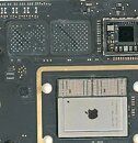
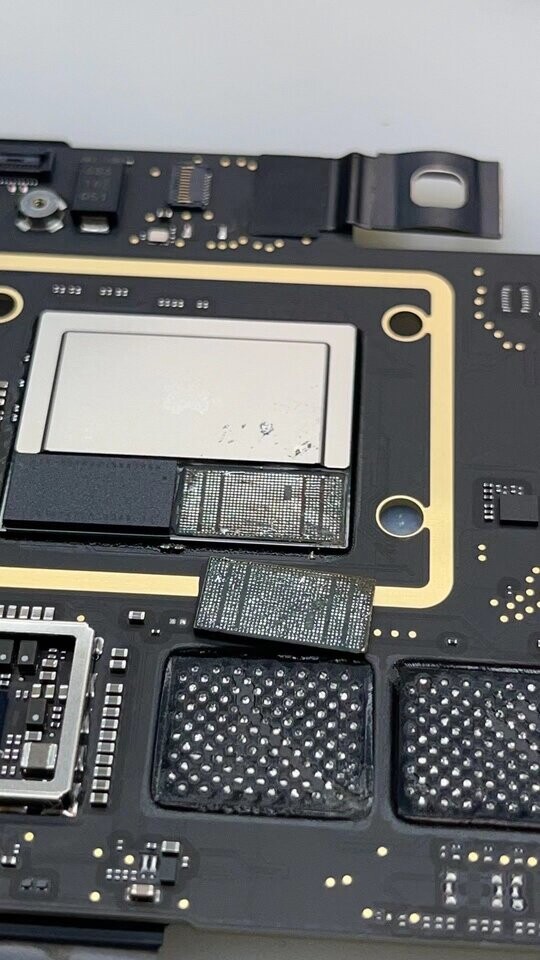
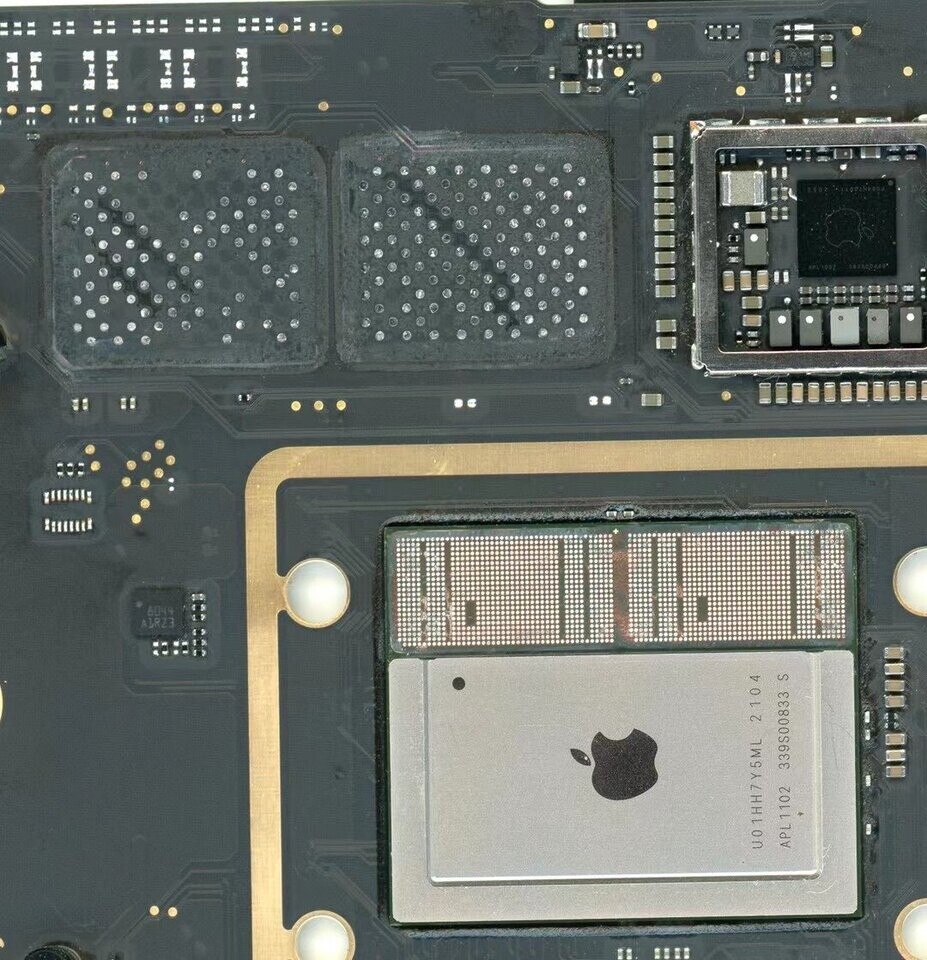
The Apple M1 processor features integrated memory directly on the chip to reduce latency, power, and size. While this design may be good for the overall user experience it does not bode well for upgradability requiring users to pay up for a more expensive model. Some Chinese engineers have recently shown how it is possible to upgrade the soldered memory and storage components given you have the time, skills, and money. The DRAM and NAND chips are soldered to the M1 chip and motherboard but can be removed and replaced with higher capacity chips using a specialty soldering station. The engineers upgraded the base model M1 Mac Mini with 8 GB RAM and 256 GB storage to 16 GB RAM and 1 TB storage. The upgrade didn't require firmware modifications according to the source which is very impressive if true.
Source: @duanrui1205
Add your own comment

16 Comments on Engineers Upgrade Soldered Components on Apple M1 Mac Mini

#1
dont whant to set it"'
Just like any internal combustion engine that has fitted to it an improper gearbox. Maybe the M1 is not up to it either way.
Posted on Reply
#2
Fouquin
I saw this earlier today and it looks sus. The images show they mutilated at least one board, and the original chinese article doesn't actually state they upgraded the DRAM or show an proof that anything was actually upgraded. Lots of fluff statements about how amazing their work was though...
Posted on Reply
#3
Totally
FouquinI saw this earlier today and it looks sus. The images show they mutilated at least one board, and the original chinese article doesn't actually state they upgraded the DRAM or show an proof that anything was actually upgraded. Lots of fluff statements about how amazing their work was though...
Those solder pads can be fixed.
Posted on Reply
#4
Fouquin
TotallyThose solder pads can be fixed.
If they were as experienced as the article claimed they wouldn't have damaged them to begin with. Not to mention the nearly exposed copper layer on the substrate...
Posted on Reply
#5
Crackong
integrated memory directly on the chip to reduce latency, power, and size. While this design may be good for the overall user experience
Come on we all knew it is 10% cost saving and 90% locking user upgradability so they can mark up the prices on higher tier options.
Posted on Reply
#6
Totally
FouquinIf they were as experienced as the article claimed they wouldn't have damaged them to begin with. Not to mention the nearly exposed copper layer on the substrate...
Do you not see how much underfill that was there from the previous pic, I'm not going to knock them for that it.
Posted on Reply
#7
wickerman
There's a rather large industry around this sort of thing already in china. Ebay is full of "x99" and "x79" motherboards using chipsets salvaged from ewaste. And its not an uncommon thing to have the flash storage on a phone upgraded for you by a booth at a mall or a storefront similar to a cell phone repair store that swaps glass all day.

I'm all for it and think this sort of thing is what we need from Nvidia and AMD right now. I'm sure they could have some kind of buy back/salvage deal with big crypto miners to take back cards once they are no longer in that perfect efficiency curve to be profitable, and salvage the gpu and memory (after validation) for new boards they can sell with a warranty. All those old p106 mining cards with no video outputs could become gtx 1060s.
Posted on Reply
#8
Caring1
wickermanThere's a rather large industry around this sort of thing already in china. Ebay is full of "x99" and "x79" motherboards using chipsets salvaged from ewaste. And its not an uncommon thing to have the flash storage on a phone upgraded for you by a booth at a mall or a storefront similar to a cell phone repair store that swaps glass all day.

I'm all for it and think this sort of thing is what we need from Nvidia and AMD right now. I'm sure they could have some kind of buy back/salvage deal with big crypto miners to take back cards once they are no longer in that perfect efficiency curve to be profitable, and salvage the gpu and memory (after validation) for new boards they can sell with a warranty. All those old p106 mining cards with no video outputs could become gtx 1060s.
And the P104 could be converted back to a 1080 8GB.
those cards are still value today.
Posted on Reply
#9
Fouquin
CrackongCome on we all knew it is 10% cost saving and 90% locking user upgradability so they can mark up the prices on higher tier options.
It's actually more expensive to do DRAM on package. The savings is in DRAM access latency and fewer wasted cycles allowing a bit more performance. It is entirely about squeezing more performance than anything else.
TotallyDo you not see how much underfill that was there from the previous pic, I'm not going to knock them for that it.
I am going to knock them for it. Especially when they claim to be some superior engineering team with no evidence of actually making the upgrade work. Anyone can hack off some chips with a razor.
Posted on Reply
#10
wickerman
Caring1And the P104 could be converted back to a 1080 8GB.
those cards are still value today.
Absolutely right, my old 1080 was just gifted to a friend as an upgrade and that card can do modern AAA no problem.

I just think its a reasonable idea to embrace. Nvidia and AMD can take their latest and greatest silicon and put it in the hands of miners first and have the gpu, memory, and vrms designed and tuned for mining efficiency. The only other guys paying mining prices right now are the professional compute guys with Teslas and and Quadros - and they already get silicon tuned for certain targets (Tesla T4 gets RTX 2070 super shader/tensor count but at a third the clock speed and on a half height/single slot card). Just create the eco system where last gens compute silicon becomes this gen's gaming silicon. If miners and big tensor guys want to pay nvidia 10X what gamers will pay for the latest and greatest thats fine. Reality most gamers are going to be happy with a 1080 they could get for $250. It doesnt matter that the silicon itself came out in 2016, as long as the rest of the card still works so will that GP104.
Posted on Reply
#11
Crackong
FouquinIt's actually more expensive to do DRAM on package. The savings is in DRAM access latency and fewer wasted cycles allowing a bit more performance. It is entirely about squeezing more performance than anything else.
Maybe it would be more expensive on the package side, but the overall PCB shrink + ram slot + so-dimm costs would balance that back I believe.
And still, 90% of it is to lock user upgradability.
Posted on Reply
#12
Fouquin
CrackongMaybe it would be more expensive on the package side, but the overall PCB shrink + ram slot + so-dimm costs would balance that back I believe.
And still, 90% of it is to lock user upgradability.
Apple's chosen arrangement of package on package reduces yields to nearly single digits though. So no, once you've thrown away a few million 5nm chips for a few hundred thousand working ones it's definitely not cheaper. :)
Posted on Reply
#13
birdie
Screenshots/video of a working/upgraded system, no?
Posted on Reply
#14
heky
Knowing Apple, this will get disabled with the next software/firmware update...
Posted on Reply
#15
Caring1
hekyKnowing Apple, this will get disabled with the next software/firmware update...
And then released by them at twice the price.
Posted on Reply
#16
Crackong
FouquinApple's chosen arrangement of package on package reduces yields to nearly single digits though. So no, once you've thrown away a few million 5nm chips for a few hundred thousand working ones it's definitely not cheaper. :)
May I ask the source of this ?
Near single digit yield sounds bit odd
Posted on Reply
Add your own comment
Apr 26th, 2024 12:52 EDT change timezone

New Forum Posts

Popular Reviews

Controversial News Posts