Wednesday, November 17th 2021

Fujitsu Launches New 8Mbit FRAM Guaranteeing Writing Endurance up to 100 Trillion Times
Fujitsu Semiconductor Memory Solution Limited has launched new 8 Mbit FRAM MB85R8M2TA with parallel interface, which is the first product to guarantee 100 trillion read/write cycle times in Fujitsu's FRAM product family. Evaluation samples are currently available. The new product achieves both high-speed operations, approximately 30% faster access speed, and low power consumption, 10% less operating current, compared to Fujitsu's conventional products. This memory IC is an ideal replacement of SRAM in the industrial machines that require high-speed operation.
FRAM is a non-volatile memory product with superior features of high read/write endurance, fast writing speed operation and low power consumption, and it has been mass-produced for over 20 years. Fujitsu has been providing 8 Mbit FRAM MB85R8M2T with parallel interface since June 2018. While promoting the product, the company heard voices of customer requirements such as guaranteed writing endurance of more than 10 trillion times, operation as fast as SRAM and TSOP package compatibility to SRAM. Fujitsu is now pleased to introduce its new 8 Mbit FRAM product satisfying these requirements, maintaining FRAM's unique feature of lower power consumption. The MB85R8M2TA with an SRAM-compatible parallel interface operates at a wide range of power supply voltage from 1.8 V to 3.6 V. It is the first product that guarantees 100 trillion read/write cycle times in Fujitsu's FRAM product family.
Being capable of operating up to 25ns in fast page mode, the new FRAM's access speed is as high as SRAM at continuous data transfer. It achieves not only higher-speed operation but lower power consumption than Fujitsu's conventional FRAM product. This FRAM has the maximum write current of 18mA, 10% less than the current product, and the maximum standby current of 150µA, 50% less. It is housed in a 44-pin TSOP package which is the same package as Fujitsu's 4 Mbit FRAM in addition to a 48-pin FBGA package. The new 8Mbit FRAM brings customers the benefit of eliminating a data-backup battery necessary for SRAM in some cases. Fujitsu's FRAM product can solve the following issues arising from replacing SRAM with non-volatile memory.
 Fujitsu Semiconductor Memory Solution is committed to contribution to sustainable society while developing high-performance products. As an example, the company continues working on the development of low-power consumption FRAM products. With the reduction of power consumption, it aims to reduce CO2 emissions for less greenhouse gas.
Fujitsu will continue to satisfy the needs and requirements from the market and customers and also develop eco-friendly memory products.
Key Specifications
Part Number MB85R8M2TA
Density (configuration) 8 Mbit (512K x 16 bit)
Interface Parallel Interface (low power SRAM compatible)
Operating voltage 1.8 V to 3.6 V
Operating temperature range -40°C to +85°C
Read/Write endurance 100 trillion (1014) times
Package 48-pin FBGA, 44-pin TSOP
Low power consumption Operation current: 18mA (max.)
Standby current: 150 µA (max.)
Sleep current: 10 µA (max.)
Source:
Fujitsu Semiconductor Memory Solution
FRAM is a non-volatile memory product with superior features of high read/write endurance, fast writing speed operation and low power consumption, and it has been mass-produced for over 20 years. Fujitsu has been providing 8 Mbit FRAM MB85R8M2T with parallel interface since June 2018. While promoting the product, the company heard voices of customer requirements such as guaranteed writing endurance of more than 10 trillion times, operation as fast as SRAM and TSOP package compatibility to SRAM. Fujitsu is now pleased to introduce its new 8 Mbit FRAM product satisfying these requirements, maintaining FRAM's unique feature of lower power consumption.
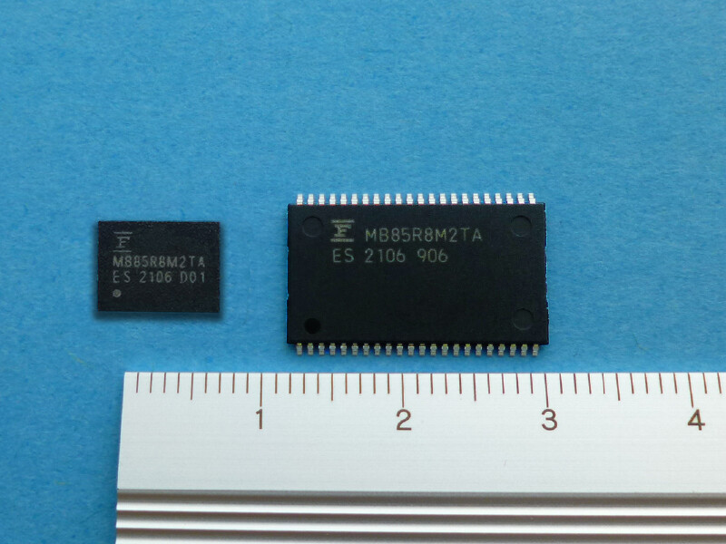
Being capable of operating up to 25ns in fast page mode, the new FRAM's access speed is as high as SRAM at continuous data transfer. It achieves not only higher-speed operation but lower power consumption than Fujitsu's conventional FRAM product. This FRAM has the maximum write current of 18mA, 10% less than the current product, and the maximum standby current of 150µA, 50% less. It is housed in a 44-pin TSOP package which is the same package as Fujitsu's 4 Mbit FRAM in addition to a 48-pin FBGA package.

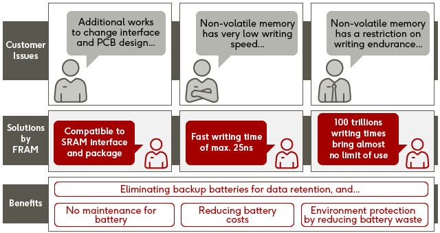
- Issue: Additional work to change interface design and PCB design
- Solution: Use of FRAM compatible with SRAM interface and SRAM package
- Issue: Difficult to replace with non-volatile memory of very slow writing speed
- Solution: Use of FRAM featuring fast writing operation as a maximum 25ns in page mode
- Issue: Design restriction due to writing endurance up to 10 trillion times
- Solution: Use of FRAM with writing endurance up to 100 trillion times
Fujitsu will continue to satisfy the needs and requirements from the market and customers and also develop eco-friendly memory products.
Key Specifications
Part Number MB85R8M2TA
Density (configuration) 8 Mbit (512K x 16 bit)
Interface Parallel Interface (low power SRAM compatible)
Operating voltage 1.8 V to 3.6 V
Operating temperature range -40°C to +85°C
Read/Write endurance 100 trillion (1014) times
Package 48-pin FBGA, 44-pin TSOP
Low power consumption Operation current: 18mA (max.)
Standby current: 150 µA (max.)
Sleep current: 10 µA (max.)
13 Comments on Fujitsu Launches New 8Mbit FRAM Guaranteeing Writing Endurance up to 100 Trillion Times
This is still your only option for nv ram with "virtually" unlimited writes.
SLC Flash: rated for 100,000 writes.
www.intel.com/content/www/us/en/architecture-and-technology/optane-technology/delivering-new-levels-of-endurance-article-brief.html
Optane is just an order-of-magnitude better (around 1.4 million writes)
I wouldn't trust to take the place of anything high-performance as far as SRAM goes
5 year rated lifetime in embedded world is nothing (especially for the price premium they charge over MLC)