Wednesday, February 11th 2026

Intel "Nova Lake" Compute Tile Die-sizes Surface
Intel is preparing to launch its next generation Core Ultra Series 4 "Nova Lake" processors in the second half of 2026. We have some hint on what the sizes of the Compute tiles of these chips could measure. "Nova Lake" remains a tile-based disaggregated chip, just like the current "Arrow Lake," with the most advanced foundry node being allocated only to the components that can benefit the most from it, the CPU cores. The CPU complex of the processor is located in the Compute tile, while low-power island E-cores are located on the SoC tile that's built on a slightly older foundry node.
Intel is building the Compute tile of "Nova Lake" on the TSMC N2 (2 nm nanosheet) foundry node. There will be different types of Compute tiles based on the CPU core count and cache sizes. The two most popular ones for the desktop platform will be the mainstream tile with 8P+16E core configuration and a standard L3 cache size shared among the eight P-cores and four E-core clusters. The second, more premium Compute tile type will be 8P+16E with bLLC, or big last-level cache. bLLC is an enlarged L3 cache that's estimated to be 3-4 times the size of the regular L3 cache. This is Intel's answer to AMD's 3D V-Cache. Estimates put the regular Compute tile to measure around 110 mm², while the premium variant with bLLC is estimated to measure over 150 mm². This 36% increase in die-area is entirely from the enlarged last-level cache.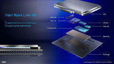 This isn't the entirety of the "Nova Lake" chip, there will be other components, such as the SoC tile that contains the low-power island E-cores, the DDR5 memory controllers, the 74 TOPS NPU, and the PCI-Express Gen 5 root complex, besides the System Agent, Management Engine, and security processor. Besides the SoC tile, are the Graphics tile, which is likely to be built on a more advanced node than the SoC, but less advanced than the Compute tile. Intel has plenty of options for the Graphics tile, including its own Intel 4 foundry node.
Source:
HXL (Twitter)
Intel is building the Compute tile of "Nova Lake" on the TSMC N2 (2 nm nanosheet) foundry node. There will be different types of Compute tiles based on the CPU core count and cache sizes. The two most popular ones for the desktop platform will be the mainstream tile with 8P+16E core configuration and a standard L3 cache size shared among the eight P-cores and four E-core clusters. The second, more premium Compute tile type will be 8P+16E with bLLC, or big last-level cache. bLLC is an enlarged L3 cache that's estimated to be 3-4 times the size of the regular L3 cache. This is Intel's answer to AMD's 3D V-Cache. Estimates put the regular Compute tile to measure around 110 mm², while the premium variant with bLLC is estimated to measure over 150 mm². This 36% increase in die-area is entirely from the enlarged last-level cache.

55 Comments on Intel "Nova Lake" Compute Tile Die-sizes Surface
Since Nova Lake is supposed to span most desktop markets creating lower end SKUs with Intel 18A CPU tile might make financial sense where TSMC N2 wouldn't have.
The flexibility of tile/chiplet designs at work ;)
It's the same reason AMD went with Global Foundry's vastly inferior 14nm process node instead of using TSMC's 16nm. They weren't making almost any CPUs at the time, but had a contract with GloFo and had to adhere to it.
That's disappointing in a way. This variant should be really expensive considering that SRAM scales awfully with node size and represents a lot of die area in such cases.
Even worse considering that there is that rumored dual compute tile config, so that means 300m²+ for those tiles alone. I wonder how big the actual chip and its socket will be.I thought that one of the complaints that folks had with ARL was that the memory controller was not on the compute tile, and thus gaming performance suffered a bit, and due to that Intel would move the memory controllers back into the compute tile. Seems like I did the wrong assumption, but having this in the SoC tile makes way more sense anyway.Being the devil's advocate here, I assume that 18A is pretty efficient, but doesn't scale that well with power/clocks, and thus it should not be that great for desktop and other higher-clocking parts. If it still manages to be really efficient with a competitive pricing, it might be a great option for mobile options (not only laptops, but phones as well), as well as dense server options, which is arguably a way larger market.
PTL will be where Intel shows if the above is true, given that it parted away with lots of decisions that made LNL hella efficient, but still touting the same efficiency at ARL levels of performance. If that pans out, I can see other players going for 14A.
Rumors point that Apple will use 18A for lower-end M-chips, and a more recent one says that MediaTek will be using 14A, those are really big wins and I can see other customers such as Qcom and AMD (for their dense/laptop offerings) following suit if TSMC doesn't reduce their pricing.This is also a great marketing strategy for their EMIB offerings, going all "hey, we can package all kinds of stuff without issues" lolAFAIK it's doing better than Samsung's current node, but I'm not sure if that says much lol
Agreed that mobile parts make more sense, adding they are not only cheaper to produce but are higher volume as well.
semiwiki.com/wikis/industry-wikis/tsmc-n2-process-technology-wiki/
Either due to power or yield issues that only make it feasible for small dies.
18A also has the issue that unlike the development that was flipped chip designs, we have gone 50% back where there are now signal layers between the transistors and heatsink. This negates some of the benefit of lower power due to BSPDN.
Modern designs that are predicated in very high clocks, voltages and have a big number of hotspots will take some work to move to 18A or the upcoming BSPDN of TSMC.
But it is a path worth taking, as it also allows redesign of the SRAM cells akin to allow for a very big increase in SRAM density that has been faltering for many years.
Mobile alone is well under 30%.
www.mordorintelligence.com/industry-reports/semiconductor-industry-landscape
I doubt Nova Lake will be cheap either with these die sizes.
From the report page it lists the entirety of the CONSUMER industry under those 30%, including mobile phones, laptops and desktop devices.
The remaining of those 70% include tons of things that do not use the latest and greatest nodes, with stuff like MCUs and power regulators, which wouldn't use a modern node by any means, so you can't compare it to what Intel is targeting.
www.ad-hoc-news.de/boerse/news/ueberblick/tsmc-apple-und-qualcomm-sichern-gesamte-2nm-produktion/68544999
Gaming - unlikely considering the kind of deficit they'll have to claw back to first match Zen 5 X3D and then Zen 6 and then Zen 6 X3D on top of that.
If they were equal today then yes they would have a good chance, but they're not. They're far behind now. Double digit percentages. I forgot the exact number, but it is bad.The gap will likely not be as big as 24 vs 52 would suggest considering more than half of these cores are far weaker than Zen 6 cores.
Also if AMD really wanted they could make a Zen 6c (dense) core available on AM5 by cutting some of the cache.
This will likely get close to the 52 core count of Intel.
Whether they'll do it or not remains to be seen as so far dense cores have only been used in server primarily and mobile occasionally.
Here's an illustration from Cadence. First is flip-chip, second is a chip with BSPDN (BSM = backside metal), third is a stack of both.
Do not underestimate the E-cores, especially the ones which come in Nova Lake. My current estimates based on aggregate FP data from PassMark has Arrow Lake E-cores around 80% as good as Zen 5 cores in IPC. Nova Lake E-cores are going to have easily double digit IPC gains according to rumors, likely to facilitate reunification of P and E cores with Titan Lake.
And you're completely wrong about the productivity benchmarks, the e cores provide far more benefit for the space they take up than a fat Zen c core.
The 285K essentially matches the 9950X in the entire application test suite. Doing so with 8 less threads (and no AVX-512) shows that e-cores are a much better way to get multi-threading power. If an 8P+16e CPU is matching a 16C/32t CPU, a 16P+36e processor will absolutely wipe the floor with a 24C/48t CPU (unless Zen 6 brings a miraculous IPC improvement).
To be clear, Zen cores are nearly half the size of comparable Coves, and the Monts are slower while taking up around the same die area (comparing half a Zen 5 8-core CCX with cache to an E-core cluster in Arrow Lake desktop). Intel is paying a price for its performance, and that's cost.