Monday, April 20th 2026

SK hynix Begins Mass Production of 192GB SOCAMM2
SK hynix Inc. (or "the company", www.skhynix.com) announced today that it has begun mass production of the 192 GB SOCAMM2, a next-generation memory module standard based on the 1cnm process (sixth-generation of the 10-nanometer technology) LPDDR5X low-power DRAM.
SOCAMM2 is a module that adapts low-power memory - which was previously used mainly in mobile products like smartphones - for server environments. It is designed to be a primary memory solution for next-generation AI servers.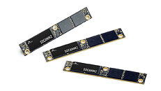
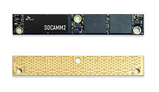
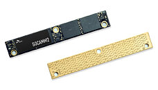 SK hynix emphasized that the 1cnm based SOCAMM2 product that is now in mass production delivers more than double the bandwidth with over 75% improved power efficiency compared to conventional RDIMM, providing an optimized solution for high performance AI operations.
In particular, the company noted that its SOCAMM2 products are designed for NVIDIA Vera Rubin platform.
SK hynix expects the new SOCAMM2 product will fundamentally resolve the memory bottlenecks encountered during the training and inference of large language model (LLM) with hundreds of billions of parameters, thereby playing a pivotal role in dramatically accelerating the processing speed of the overall system.
The company stated that with the AI market shifting focus from inference to training, SOCAMM2 is gaining significant attention as a next-generation memory solution capable of operating LLMs with low power consumption. To meet the demands of its global Cloud Service Provider (CSP) customers, SK hynix has not only been providing a supply portfolio, but also stabilized its mass production system early on.
"By supplying the 192 GB SOCAMM2, SK hynix has established a new standard for AI memory performance," Justin Kim, President & Head of AI Infra (CMO, Chief Marketing Officer) at SK hynix said. "We will solidify our position as the most trusted AI memory solution provider, through close collaboration with our global AI customers."
Source:
SK hynix
SOCAMM2 is a module that adapts low-power memory - which was previously used mainly in mobile products like smartphones - for server environments. It is designed to be a primary memory solution for next-generation AI servers.


In particular, the company noted that its SOCAMM2 products are designed for NVIDIA Vera Rubin platform.
SK hynix expects the new SOCAMM2 product will fundamentally resolve the memory bottlenecks encountered during the training and inference of large language model (LLM) with hundreds of billions of parameters, thereby playing a pivotal role in dramatically accelerating the processing speed of the overall system.
The company stated that with the AI market shifting focus from inference to training, SOCAMM2 is gaining significant attention as a next-generation memory solution capable of operating LLMs with low power consumption. To meet the demands of its global Cloud Service Provider (CSP) customers, SK hynix has not only been providing a supply portfolio, but also stabilized its mass production system early on.
"By supplying the 192 GB SOCAMM2, SK hynix has established a new standard for AI memory performance," Justin Kim, President & Head of AI Infra (CMO, Chief Marketing Officer) at SK hynix said. "We will solidify our position as the most trusted AI memory solution provider, through close collaboration with our global AI customers."
14 Comments on SK hynix Begins Mass Production of 192GB SOCAMM2
Using LPDDR5X instead of regular DDR5 makes sense in many ways, especially regarding power consumption and heat generation.
Sure, instead of scrificing it to our AI overlord it could be better used in real-world scenarios in the field like notebooks, tablets, smartphones etc.
In other words (without all the techno-babble)........
more unobtainium (at least for us little people), thanks to, well you guessed it, A.friggin.I :(
The dram technology depends on the memory controller regardless of the cpu or motherboard in question. no one prevents amd to allow low power ddr5 on consumer motherboards with all the issues and flaws.
The answer.
TPU seems to agree but I haven't seen anything more specific than this:
www.techpowerup.com/339178/ddr6-memory-arrives-in-2027-with-8-800-17-600-mt-s-speeds
So, instead of selling Nvidia a bunch of bare LPDDR ICs, they'll solder those into that SOCAMM2 PCB and sell it to Nvidia or any other OEM.
However, one chip package is 32 bits wide, not 16, because a SOCAMM is 128 bits wide.
LPDDR5/5X has an array configuration which covers the entire package, but this doesn't correlate to the die being used to make up the package. So 16GB 32-bit LPDDR5X is has a 4Gx32 configuration, but it uses 8x 2Gx8 die in a dual channel dual rank configuration to make up that package. This is where my mistake happened because I assumed it was like DDR5 where the configuration directly relates to the die being used.