News Posts matching #SK hynix

Return to Keyword Browsing

Terafab Wants to Become One of the Largest Memory Makers by 2032

According to Nikkei, a procurement team from Terafab, the chip venture between Tesla and SpaceX, visited Japan and walked local equipment makers through what it plans to buy. The targets it reportedly shared are gigantic: 1 million wafers per month from 2032 onward, with around 700,000 of those going to memory chips and 300,000 to logic. Nikkei's headline puts that at 40 times the output of Japan's Rapidus. The same split first surfaced in a Jiji Press report last month, which said a single Texas plant would handle both memory and logic, with a pilot fab completed as early as July 2027. Intel is reportedly helping with logic using its 2 nm and 1.4 nm-class technology, while a Taiwanese company has been floated as a technology partner for memory. That could be Nanya, though nothing is confirmed.

For context, Samsung's entire DRAM output was estimated at 650,000 to 700,000 wafers a month late last year, while SK hynix was at about 550,000 earlier this year and hopes to reach roughly 1 million by 2030 or 2031. It isn't clear whether Terafab's memory figure covers DRAM alone or also includes NAND, so the Samsung comparison is a loose one. Musk has also been careful with his own dates. On an October SpaceX call, he put "big error bars" on reaching volume production by Q3 2028, with a first SRAM test chip planned for mid-2027 at Terafab's Austin research lab.

The Worst Is Yet to Come for Memory Shortages, Warns Team Group

We might not be past the worst part of the global memory shortages, as the most severe supply chain squeeze could happen soon. During Team Group's earnings conference on November 2, the company stated that the worst period in memory demand is projected to be between Q4 2026 and Q2 2027, which is just a few months away. Major memory makers such as SK hynix, Samsung, and Micron have sold out their 2027 supply and entered into long-term agreements with customers, making it increasingly difficult to source memory for any third-party purposes. Team Group states that even if you have the funds, it might be impossible to purchase memory products. Currently, it is possible to buy memory, albeit at a high price, but soon enough, that may no longer be an option, noted the company.

Even though CXMT and YMTC are supplying close to 10% of the memory market share with their products, it is still impossible to satisfy demand. A supply-demand balance may not emerge until the second half of 2028 or even later. Currently, Team Group sells most of its memory modules to businesses in the B2B sector, which commands 64.6%, while the B2C sector, selling directly to consumers, accounts for 35.4%. This is a sharp reversal compared to the 2025 Q3 figures, where B2B was 24.6% and B2C was 75.4%. Most of the revenue now comes from the business sector developing AI servers, rather than traditional consumer purchases.

Samsung Hosts OpenAI's Sam Altman for AI Seminar, No Supply Deal Announced

Two days after arguing that the DRAM in home PCs would be put to better use in data centers, OpenAI CEO Sam Altman sat down with around 50 Samsung presidents on Saturday, October 31. The group went well past the chip business, with leaders from Samsung's finance and biotech arms joining the electronics side at the company's training center in Yongin. Samsung presented it as part of a leadership seminar series for its company-wide AI push, and the talks apparently covered where AI is headed, the markets it could open up, and how it changes the way large companies make decisions. According to Samsung, Altman told the room that adopting AI alone doesn't give anyone an edge, and that the payoff comes from using it to move faster and build better products.

Nothing came out of it in terms of a new supply contract, at least publicly, and Samsung's own write-up stuck to AI strategy. Still, it's hard to look at the visit separately from the memory shortage. Samsung signed a letter of intent with OpenAI back in October 2025 to act as a memory partner for Stargate, with OpenAI's demand projected at up to 900,000 DRAM wafers per month. Separately, on October 31, SK Group chairman Chey Tae-won also reportedly met Altman in Seoul, with SK hynix and SK Telecom executives joining, according to industry sources. Last month, AMD's Lisa Su spent hours with Samsung's chip chief chasing HBM supply, and amid all these meetings, Micron's CEO expects the memory crunch to get worse in 2027 and 2028. It seems like every major buyer is knocking on the same Korean doors.

OpenAI CEO Argues Home PCs Waste the World's Limited DRAM Supply

OpenAI CEO Sam Altman thinks the DRAM sitting inside personal computers would be better used in data centers. He made the comments on the Cheeky Pint podcast, hosted by Stripe co-founder John Collison, in an episode released on October 29. The two were discussing the memory supply chain when the topic turned to local inference, meaning running AI models on your own hardware instead of the cloud. Here's what Altman said, at roughly the 29-minute mark:
Sam Altman, OpenAI CEOA lot of people want local inference. And somehow, they assume that the problem is solved now. Because, we are going to have open-source models. We're going to be able to run them on our computers. And so we're not going to need all the stuff in the data center. But from a global allocation perspective, actually, it's quite terrible to have everybody have a bunch of the world's limited supply of DRAM sitting in their own computer. And, being used 5% of the time. You want maximum utilization in the cloud if you're trying to deal with this very supply constrained environment. And somehow everyone's... many people's intuition is the opposite of that.

Solidigm Considers $45 Billion Investment in U.S. NAND Flash Manufacturing

Late last month, we learned that SK hynix-owned NAND Flash maker Solidigm has been considering expanding its manufacturing business to the United States. According to Bloomberg, the company is contemplating a massive $45 billion investment. However, before deciding on that, Solidigm aims to get approval from the U.S. government to send equipment to its fabs in Dalian, China, so it can continue funding expansion in the United States. As a reminder, obtaining some chipmaking equipment in China requires U.S. government approval, meaning the company is putting things on hold pending regulatory approval.

Currently, Solidigm operates Fab 1 in Dalian, China, and has accelerated the construction of Fab 2 nearby. This expansion aims to increase production by 50% by 2027 to meet the rising demand for NAND Flash. Solidigm owns and operates this facility, marking a resumption of expansion in mainland China after a four-year project freeze. At present, Solidigm produces about 100,000 wafers per month of NAND Flash, so a 50% increase by 2027 would boost production to approximately 150,000 wafers per month.

CXMT to Start HBM3E Mass Production by the End of 2026

CXMT is expected to start mass production of its first-ever HBM memory in the HBM3E form factor. According to an exclusive report from Reuters, this mass production is anticipated to begin within the next two months, meaning CXMT will officially start by the end of the year. Back in August, CXMT began risk production of HBM3E memory. However, the company has struggled with the yield of HBM3E memory modules, and this situation remains similar today, according to the latest report. While we don't have specific performance details, JEDEC's official data for HBM3E indicates a 1,024-bit width and speeds ranging from 9.2 Gbps per pin to 12.4 Gbps, with most standard configurations targeting 9.6 Gbps per pin. The total bandwidth is around 1.2 TB/s, and capacities range from 24 GB using 8-high stacks to 36 GB using 12-high stacks of 24 Gb layers.

CXMT's main challenge lies in the immaturity of the through-silicon via (TSV) technology it employs. In front-end manufacturing, CXMT achieves around 30% yields, while back-end processing adds about 70% on top of the original 30%. For example, Samsung uses about 5,000 TSVs per layer on HBM2, and SK hynix uses more than 8,000 TSVs per layer on its HBM3. However, data suggests that CXMT is attempting to achieve HBM3E with only 3,000 TSVs per layer and is trying to pack 8 layers into the regular 8-high HBM3E configuration. Given these challenges, the company is unlikely to transition to a higher-capacity 12-high HBM in the near term as it addresses engineering issues.

SK hynix Expects Memory Demand to Outpace Supply Through 2030

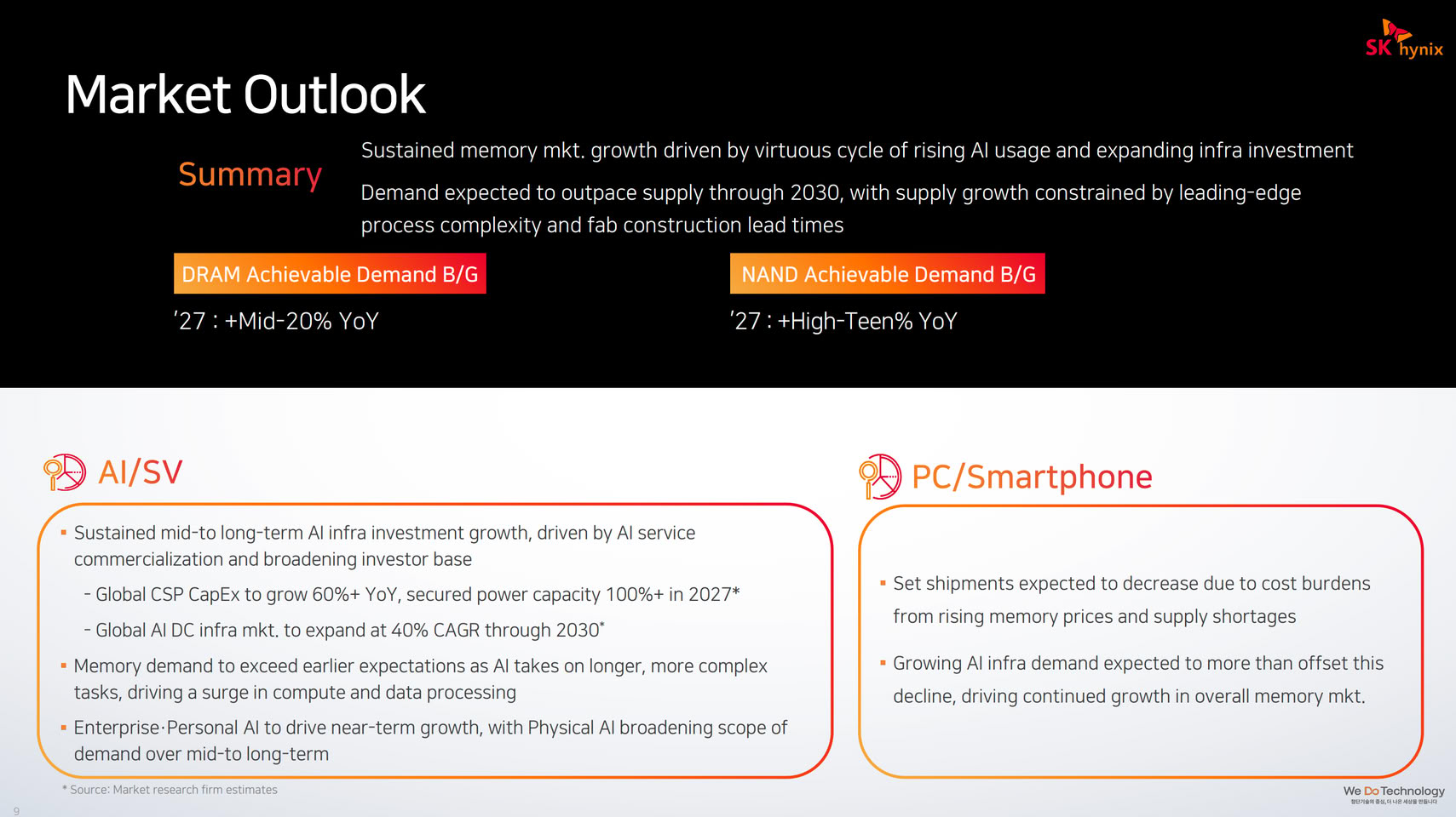
SK hynix reported its latest Q3 2026 quarterly results with a record $78.129 billion in net revenue. However, the company also shared a market outlook, highlighting its long-term supply agreements and plans for expansion with new fab capacity and facilities under construction. For the consumer market, the outlook is grim as SK hynix expects memory demand to continue outpacing supply through 2030. The main supply constraint is the complexity of leading-edge semiconductor nodes and the lengthy lead times for fab construction, which take years to translate into regular mass production volumes.

Despite sustained demand, pricing is also on an upward trajectory, with the average selling price of memory modules in Q3 increasing by over 20% compared to Q2. This is concerning, as it suggests that the prices of consumer electronics devices might jump by more than 20% once memory inventory is depleted. Although SK hynix expects a decrease in PC and smartphone shipments, this will be offset by a strong rollout of AI data centers. About 14 major customers, including most hyperscalers, have signed 5-year long-term agreements, which will account for over 50% of total capacity sold for 2027 and 2028.

SK hynix Announces 3Q26 Financial Results

SK hynix Inc. announced today that it has recorded 104.6155 trillion won in revenues, 83.3338 trillion won in operating profit (with an operating margin of 80%), and 39.7756 trillion won in net profit (with a net margin of 38%) in the third quarter. In a market environment in which prices of key products have risen on the back of growing demand for AI memory, the company once again posted all-time-high quarterly results in both revenue and operating profit, underpinned by the competitiveness of its high-value-added products. In particular, revenue exceeded 100 trillion won for the first time in the company's history. Revenue and operating profit increased by 32% and 38%, from the previous quarter, respectively.

By product, DRAM results were driven by a significant increase in sales of server DDR5 while HBM4 shipments began in earnest. In NAND, sales of 321-layer TLC eSSD expanded, and high-value-added products for data centers continued to grow across the board. The company's financial structure has also become significantly concrete. At the end of the third quarter, cash and cash equivalents stood at 114.5 trillion won, up 26.5 trillion won from the end of the previous quarter, while borrowings decreased by 2.8 trillion won to 15.8 trillion won. As a result, net cash increased to 98.7 trillion won.

Micron Walks Away From 4F² DRAM After Two Decades of Research, Bets on 3D DRAM Instead

Micron has decided not to bring 4F² DRAM to market, even though it says it invented the cell design and has been researching it for around two decades. Scott DeBoer, Micron's President and Chief Technology and Products Officer, shared the decision during the company's technology webinar on October 21. On paper, 4F² uses vertical channel transistors to shrink each memory cell's footprint by about a third compared with the 6F² layout used in today's DRAM. However, DeBoer argued that real-world density is limited by how closely the capacitors can be packed, not by the cell's footprint, calling the density advantage over 6F² "a bit of a myth." He also said 4F² can be built, but at a higher cost and complexity, and that it runs into fundamental scaling problems at leading-edge nodes, which points toward 3D DRAM instead.

That puts Micron at odds with its rivals. Samsung and SK hynix are both developing 4F² designs, and China's CXMT says its first 4F² product will be a server DDR5 RDIMM due by the end of this year. Micron will keep scaling 6F² instead, with its 1-delta node set to ramp in Boise, Idaho, in the second half of 2027 and the 1-epsilon node after it moving to wafer bonding. 3D DRAM is being developed as a parallel path, but there's no timeline yet, and Micron says it will only switch once the economics make sense. It's a risky bet if rivals manage to make 4F² cheap at scale, especially with memory supply expected to get even tighter in 2027 and 2028, per Micron's own estimates.

Dell CEO Says the Memory Shortage Will Get Worse in 2027

Michael Dell doesn't think the memory shortage is anywhere near over. Speaking with The Wall Street Journal, Dell's chairman and CEO said things will get worse next year, as the AI data center buildout keeps soaking up DRAM and HBM supply. According to him, the bottleneck for Dell isn't demand, since the company is sitting on roughly $95 billion worth of AI server orders it hasn't delivered yet, the largest backlog in its history. Memory is what's holding those shipments back, as AI accelerators need plenty of HBM, while the servers around them still rely on conventional DRAM.

Relief also looks quite far away. New memory fabs take around four years to build, so Dell apparently doesn't expect meaningful new supply until 2029 or 2030. That aligns with Micron's CEO, who recently said supply will be much tighter in 2027 and 2028 than it is this year. Interestingly, SK hynix's CEO said something similar, expecting the memory shortage to last through 2030. Dell is reportedly coping by buying DRAM only when final assembly is close and by locking in long-term supply agreements, though there's no word on how much of that applies to its consumer products.

XCENA Showcases CXL Memory Innovations for AI Inference at OCP Global Summit 2026

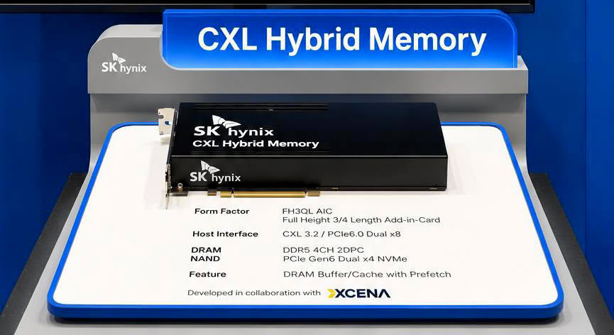
XCENA, a fabless semiconductor company developing next-generation memory infrastructure for the AI era, demonstrated its CXL-based memory solutions for AI inference demonstrations at OCP Global Summit 2026, addressing AI inference's growing memory requirements and data-movement burden. The event was held Oct. 12-15 at the San Jose McEnery Convention Center. The demonstrations address two of the biggest constraints on AI inference: growing memory requirements and the cost of moving data.

XCENA showed two AI inference use cases built on MX1, its Compute Express Link (CXL)-based computational memory solution.

SK hynix Reportedly Faces Difficulties in HBM Hybrid Bonding, Trailing Samsung

According to a process development engineer at SK hynix's future technology research institute, who spoke with Damnang, SK hynix is reportedly facing challenges in developing hybrid bonding technology for its HBM memory. These issues are significant enough that SK hynix has not yet begun production of samples, while Samsung has reportedly already sent out samples of HBM manufactured using hybrid bonding to customers. If true, this represents a major setback for SK hynix, whose HBM has held the top spot in global market share by revenue. This could potentially lead to a loss of market share among customers who require higher capacities, better performance, and more advanced technology from their HBM suppliers.

For those unfamiliar, hybrid bonding creates a permanent bond between two silicon chips using embedded metal bumps that are fused together to form a single chip. Multiple dies or entire silicon wafers can be connected by stacking the back ends of two chips together. This technology eliminates traditional chip bumps and directly bonds copper interconnections between the two chips. Essentially, hybrid bonding can create shorter distances, reducing latency and improving performance, lowering signal distortion, and offering many other benefits.

NVIDIA Could Account for 37% of 2027 HBM Capacity, Worth $279 Billion

NVIDIA's supply commitments climbed to $279 billion in the quarter ended July 26, up from $119 billion the quarter before. The company says the increase is primarily related to memory procurement. Morgan Stanley estimates that NVIDIA has claimed about 37.3% of global high-bandwidth memory (HBM) supply for 2027, with Alphabet at 36% and AMD at 12.1%. That adds up to roughly 85%, leaving everyone else to split the rest. These are Morgan Stanley's estimates, as reported by The Inference.

About $267 billion of the commitments come due by the end of fiscal 2029, according to the filing. NVIDIA reported record revenue of $96.2 billion for the quarter, but memory costs are weighing on margins. Gross margin was 75% and is guided to 74% this quarter, with a trough of 71% to 72% expected in the January quarter. CFO Colette Kress tied that pressure to memory pricing. Operating cash flow also fell to $24.1 billion from $50.3 billion the quarter before. Jensen Huang said on September 17 that he expects NVIDIA to sell twice as many chips next year, and the company's formal guidance is about 70% revenue growth.

Solidigm Reportedly Plans Its First NAND Fab in the United States

SK hynix subsidiary Solidigm is reportedly planning to open its first NAND Flash manufacturing facility in the United States. To address global supply chain challenges, SK hynix is exploring ways to expand its production capabilities worldwide and create a more resilient operation against geopolitical events. Currently, Solidigm operates in the United States with its headquarters and R&D center, while all its manufacturing is based outside the country. When SK hynix acquired Intel's NAND Flash manufacturing business in 2021 and established the Solidigm brand, the company continued manufacturing in China without expanding overseas.

At present, Solidigm operates Fab 1 in Dalian, China, and has accelerated the construction of Fab 2 nearby. This expansion aims to increase production by 50% by 2027 to meet the rising demand for NAND Flash. Solidigm owns and operates this facility, marking a resumption of expansion in mainland China after a four-year project freeze.

Intel and SK hynix Could Start DRAM Production in United States

According to anonymous sources close to Reuters, Intel and SK hynix are in talks to start DRAM production lines in the United States for the first time. This means that Intel might either collaborate with SK hynix to acquire memory IP technology in a joint venture or SK hynix could lease part of Intel's facility in Ohio. In the first scenario, a joint venture between Intel and SK hynix would significantly alleviate supply chain pressures, as hyperscalers, fabless chip designers, and others are in urgent need of more DRAM. Since these firms would likely consume all the DRAM produced in the coming years, both Intel and SK hynix would have a substantial financial interest in the joint venture.

On the other hand, if SK hynix decides to lease Intel's facilities in Ohio, the South Korean memory giant would pay premiums for leasing the facility while retaining all production for itself. Reuters couldn't determine which specific technology would be the focus of the facility, but the primary goal is to produce regular planar DRAM, HBM, and some storage solutions with NAND Flash. Intel declined to comment on the rumor but noted that the Ohio investments are continuing regardless. SK hynix stated that the company has not finalized its decision or any cooperation but did not explicitly rule out the possibility of future collaboration. Therefore, an official decision should be announced soon.

CXMT Reportedly Struggles With HBM3E, Yields Are Only 25%

Chinese memory giant CXMT is reportedly facing difficulties with HBM3 production, according to South Korean media. Late last month, it was revealed that CXMT had begun risk production of HBM3E memory, lagging two generations behind Samsung, SK hynix, and Micron, who are already progressing with HBM4E sampling. At that time, it was known that the company was conducting HBM3E risk production in limited runs, but details were scarce. However, today we learn that three out of four HBM3E stacks are defective, indicating that CXMT currently operates at a 25% yield. Stacking DRAM is a complex task, as the technology required is much more intricate than planar DRAM manufacturing, an area where CXMT reportedly excels.

The low yields are reportedly due to the immaturity of the through-silicon via (TSV) technology that CXMT employs. In front-end manufacturing, CXMT achieves around 30% yields, while back-end processing yields about 70% on top of the original 30%. For instance, Samsung uses about 5,000 TSVs per layer on HBM2, and SK hynix uses more than 8,000 TSVs per layer on its HBM3. However, data suggests that CXMT is attempting to achieve HBM3E with only 3,000 TSVs per layer and is trying to pack 8 layers in the regular 8-Hi HBM3E configuration. Given these challenges, the company is unlikely to transition to a higher-capacity 12-Hi HBM in the near term as it addresses engineering challenges.

SK hynix Boosts Leading-Edge 1c DRAM Production to a Dominant Position

SK hynix is shifting much of its capacity to the latest 1c DRAM node, according to recent reports. The South Korean giant is transitioning the bulk of its memory production between nodes, and as DRAM technology advances, the company is moving its production to more advanced 10 nm-class nodes. For SK hynix, the sixth-generation 10 nm class 1c DRAM node accounted for 10% of production in Q1 2026, with an increase to about 13% in Q2. In the current third quarter, the company is expected to manufacture 24% of its DRAM on 1c, while Q4 will see more than a third (34%) produced on that node. By Q1 2027, the 1c node will account for around 35%, making the fifth-generation 10 nm-class 1b node at 33%, officially SK hynix's most dominant node.

As a reminder, DRAM nodes are not the same as conventional logic nodes. DRAM manufacturers use variations of 10 nm and scale them with more EUV layers or advanced features. For SK hynix, the currently dominant 1b node is around 12-13 nm in actual design and involves about 4 layers of EUV patterning, while the most advanced 1c node shrinks to 11-12 nm with 5-6 layers of EUV. SK hynix will use the 1c node to manufacture HBM4E, LPDDR6, and DDR5 memory. For the older 1b node, SK hynix produces DDR5, LPDDR5X, HBM3E, and HBM4.

CXMT Officially Starts Mass Production of LPDDR6 Memory

CXMT has achieved the remarkable feat of officially beginning high-volume manufacturing of LPDDR6 memory. This positions CXMT's LPDDR6 memory modules as some of the first in the industry, with South Korean memory makers on a similar timeline for volume production of this next-generation technology. Reportedly, Xiaomi is the first customer for CXMT's domestic LPDDR6 memory, set to feature in the upcoming Xiaomi 18 Fold smartphone. Since the Xiaomi 18 Fold is scheduled to launch in September, CXMT's LPDDR6 memory will need to be delivered before the end of the month, indicating that customer shipments are already underway. This news follows recent reports that CXMT is conducting risk production of LPDDR6, suggesting a very high yield in production.

CXMT's LPDDR6 memory will operate at speeds of up to 12.8 Gbps, with the base speed of LPDDR6 being 10.7 Gbps. LPDDR6 builds on where LPDDR5X left off, which could reach speeds of up to 10.7 Gbps when highly overclocked. However, the new standard aims for significantly higher speeds, with the first generation of LPDDR6 from CXMT's fabs reaching 12.8 Gbps. Additionally, CXMT is producing these chips with a 16 Gb capacity, equivalent to 2 GB, and the memory IC is housed in a package-on-package (POP) casing, featuring about 1,295 pins in a ball grid array.
Update, 14:55 UTC, September 7th : CXMT's official website confirmed mass production, with Alibaba Cloud, ByteDance, Tencent, Lenovo, Transsion, Honor, Vivo, and Oppo as customers.

DRAM Industry Revenue Rises 59.5% QoQ in 2Q26 as Supply Expansion Continues to Lag Demand Growth

TrendForce's latest findings on the memory industry reveal that sharp rises in traditional DRAM contract prices have led to a 59.5% QoQ increase in total DRAM industry revenue, reaching nearly US$154.73 billion in 2Q26.

Growing demand for AI servers, fueled by expanding LLM training and AI inference, has driven higher shipments of HBM3e, LPDDR5X, and high-capacity RDIMMS. The surge in agentic AI applications is further boosting RDIMM demand across various capacities.

Samsung Foundry Allocates Half of 4 nm Capacity for HBM4 Base Dies

According to Korean media, Samsung Foundry, a division that operates silicon manufacturing as a subsidiary of Samsung Electronics, is reportedly allocating significant capacity for HBM4 base die manufacturing. For HBM4, Samsung is producing the base die on a 4 nm node, which reportedly receives half of the entire manufacturing capacity of the 4 nm node, internally referred to as SF4. Customers of HBM4 and the upcoming HBM4E memory standards are now requesting base dies to be filled with custom logic. For instance, customers could implement custom logic like memory controllers and PHYs directly on the HBM base die, significantly reducing the area occupied by these components on the main compute chiplet.

Samsung operates its SF4 manufacturing at Pyeongtaek Campus 2 (P2) and Campus 3 (P3) on lines S5 and S6. An increase in manufacturing is not only coming for ASIC designs by external customers but also for HBM4 base die manufacturing, which is becoming especially important for ASIC customers aiming to maximize the performance of their designs.

Samsung Leads NAND Market as Prices Climb 55% in a Single Quarter

The latest NAND market share data from Counterpoint Research shows just how far prices have risen in 2026. The global NAND market grew 70% quarter-over-quarter in Q2, following 90% growth in Q1. This is driven almost entirely by rising prices rather than higher shipments. NAND contract prices climbed 55% QoQ in Q2 alone, which lines up with earlier TrendForce estimates pointing to a 70-75% jump over the same stretch. Samsung held onto the top spot with 28% revenue share, down slightly from 29% in Q1 and 32% a year earlier, while SK hynix sits second at 19% and Micron rounds out the top three at 15%, helped along by high selling prices.

The surge traces back to AI infrastructure eating up NAND supply that would otherwise go toward consumer SSDs. Enterprise and hyperscale buyers are stockpiling high-capacity flash for AI servers, and manufacturers have leaned into that shift since it carries far better margins than retail drives. That's left less capacity for client SSDs, and it's part of why consumer drive prices keep climbing even as shipment volumes stay flat. China's YMTC is one of the more interesting movers here, growing from a 9% share a year ago to 14% in Q2, likely picking up volume as the bigger three chase their most profitable enterprise orders instead. Most forecasts still put meaningful price stabilization sometime in 2027, since new NAND capacity takes years to bring online and AI demand shows no sign of slowing.

CXMT Captures 10% of the Global DRAM Market Revenue Share

According to Counterpoint Research trackers, Chinese memory giant CXMT captured 10% of the global DRAM market share by revenue in Q2 2026, which is 150% more than the company had a year ago. On a quarterly basis, the company also experienced significant growth of 25%, as it increased its market share from 8% in Q1 to 10% in Q2. This is impressive considering the company managed to grow its revenue market share despite constrained access to advanced tooling, while established giants like Samsung, SK hynix, and Micron have undisputed access to all semiconductor manufacturing tools.

Among other DRAM makers, Samsung retains the number one spot with a 38% share, SK hynix holds 25%, and Micron is just behind at 24%. Interestingly, over the last few quarters, Samsung managed to maintain and grow its number one position, while SK hynix's share dropped from 39% a year ago to the current 25%. Micron fluctuated between 22% and the current 24%, while Nanya doubled its share from 1% to 2%.

TSMC Delays Hybrid Bonding Investment for HBM, Opts for Microbumps

According to the latest report from ETNews, citing supply chain sources, TSMC is reportedly still holding back from investing in the silicon packaging technology known as hybrid bonding for HBM memory integration. For those unfamiliar, hybrid bonding creates a permanent bond between two silicon chips using embedded metal bumps that are fused together to form a single chip. Multiple dies or entire silicon wafers can be connected by stacking the back ends of two chips together. This technology eliminates traditional chip bumps and directly bonds copper interconnections between the two chips. In modern packaging, chip solder bumps, which stick out before the chip is soldered to the PCB, are roughly 100 micrometers in size, while microbumps are approximately 20 micrometers. Hybrid bonding reduces this size to 1 micrometer. Microbumps are used to interconnect silicon with other chips inside a package, as seen in CoWoS-S and CoWoS-L, where microbumps are prevalent for chip-to-interposer connections.

For TSMC, the future may involve bypassing hybrid bonding technology for packaging HBM memory and investing in microbumps that are 5 micrometers in size. Reportedly, TSMC is preparing its supply chain for 5-micrometer microbumps, which will be even smaller than what is currently available, to enhance performance in packaging. South Korean and Japanese suppliers are reportedly collaborating with TSMC to achieve this, with mass production of 5-micrometer microbumps expected in the second half of 2028. As a reminder, AMD's 3D V-Cache technology uses hybrid bonding to put SRAM on top of logic, but TSMC reportedly plans to keep integration of HBM memory into packaging on microbumps for now.

Micron Explores Near-GPU NAND Flash to Run Bigger LLMs

Micron is reportedly exploring the idea of developing high-endurance NAND Flash modules that would be positioned closer to the GPU, rather than being located far away in the storage pool behind multiple protocols. The company is said to be investigating ways to bring NAND Flash closer to handle workloads that don't require the latency and bandwidth of traditional HBM or regular DRAM modules. This architecture, currently referred to as "near-GPU NAND," would serve as a middle ground between density and durability. This concept would allow GPUs to access a pool of NAND Flash that has a lower density than conventional TLC or QLC NAND, but instead focuses on improving I/O speeds, bandwidth, and read times.

For instance, this would enable a GPU to access a potential storage pool with hundreds of gigabytes of storage directly on the GPU package or PCB, similar to what DRAM like HBM or GDDR7/LPDDR6 already does. This tier would sit between GPU memory and regular system storage, acting as a very fast buffer, which would be ideal for the inference of massive LLMs. At that point, LLMs wouldn't be memory-bound and could run on systems with fewer GPUs, but with more storage and memory tiers to compensate for the required inference size. Additionally, this NAND would be significantly cheaper than HBM or regular DRAM and would be sized according to system specifications. Images below are HBF slides from SK hynix and Sandisk.

Samsung New Memory Roadmap: HBM5 Aims for 2x Performance, zHBM for 8x

Samsung presented its updated memory roadmap at SEMICON Taiwan 2026, with HBM5 and the upcoming zHBM architecture being the main focus points while setting ambitious goals and expectations. According to Samsung, HBM5 is targeting twice the performance and 20% higher performance per watt compared to HBM4E, alongside a 20% reduction in thermal resistance. As changes, the base die moves from the 4 nm process used in HBM4 and HBM4E to Samsung's in-house 2 nm node, and the stack options expand to 12, 16, and 20 layers. Mass production is expected around 2028. Recently, Samsung confirmed at the Hot Chips 2026 conference's Advance Program that the company is preparing to ship HBM4E memory with speeds of 16 Gbps per pin. Samsung is currently shipping HBM4 that works at 11.7 Gbps per pin.

zHBM uses a more radical approach, rather than placing memory beside the accelerator as conventional HBM does, zHBM stacks memory directly on top of the processor, shortening the data path and delivering higher bandwidth and efficiency. With zHBM, Samsung is targeting eight times the raw performance and three times the performance per watt of HBM4E, with thermal resistance reduced by 75-90%. At FMS 2026, Samsung unveiled the industry's first concept models of zHBM and is expected to launch this completely different architecture after 2029. Rethinking the HBM architecture appears to be the direction the industry is heading. NVIDIA recently announced its own NVHBM custom memory that moves the memory controller into the HBM base die rather than keeping it on the compute die.
Return to Keyword Browsing
Nov 11th, 2026 03:50 CST change timezone

New Forum Posts

Popular Reviews

TPU on YouTube

Controversial News Posts