Wednesday, May 13th 2026

Apple Taps Intel 18A-P Node for M7 MacBook Chip, 14A Node for iPhone
According to the sell-side equity research firm GF Securities, Apple is set to utilize both Intel's 18A-P and 14A nodes for its product lineups. As previously reported, the company will employ Intel's advanced 18A-P node for the M7 SoCs that power MacBook Air and entry-level MacBook Pro laptops. Intel's investment in the development and manufacturing ramp of the 14A node will also be beneficial, as Apple plans to use the 14A node for producing A21 SoCs for iPhones. The 18A-P node is ideal for Apple's laptop SoCs, providing a balance between efficiency and speed. It offers a 9% performance increase at the same power level or achieves 18% power savings at the same performance level compared to the standard 18A node, resulting in laptops with good frequency and low power usage. With Apple moving away from TSMC's 3 nm node in the current M5 SoC, the improvements will be significant and are expected to be realized by 2027.
For the A21 iPhone SoCs, Apple will use Intel's advanced 14A node, which promises a generational leap in density, frequency, and power savings. Apple's primary goal is to employ a more advanced node for mobile devices, with plans to have these chips ready by 2028. As this is anticipated to begin in about two years, Apple will likely wait for the final 14A PDK before starting trial production. It remains uncertain whether the company will manufacture its A21 Pro SoC at TSMC and leave the regular version to Intel. However, Apple is gradually diversifying its supply chain with more silicon manufacturers. With advanced packaging, Intel can compete with TSMC in many areas, and we are eager to see the outcomes of this competition.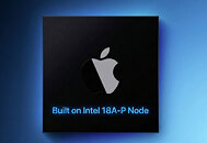
Finally, Apple's solutions might require some packaging techniques to meet the expected performance of the M7 SoC. This could involve a combination of the Foveros family, including Foveros-S, R, B, or Foveros Direct, paired with EMIB. These options offer interposers and RDL options, along with true 3D stacking using Cu-to-Cu hybrid bonding, for scenarios that demand extreme die-to-die bandwidth or power efficiency. Additionally, small silicon EMIB bridges are available in variants like EMIB-M, with embedded MIM capacitors, and EMIB-T, with TSVs.
Source:
via Juakn05 on X
For the A21 iPhone SoCs, Apple will use Intel's advanced 14A node, which promises a generational leap in density, frequency, and power savings. Apple's primary goal is to employ a more advanced node for mobile devices, with plans to have these chips ready by 2028. As this is anticipated to begin in about two years, Apple will likely wait for the final 14A PDK before starting trial production. It remains uncertain whether the company will manufacture its A21 Pro SoC at TSMC and leave the regular version to Intel. However, Apple is gradually diversifying its supply chain with more silicon manufacturers. With advanced packaging, Intel can compete with TSMC in many areas, and we are eager to see the outcomes of this competition.

19 Comments on Apple Taps Intel 18A-P Node for M7 MacBook Chip, 14A Node for iPhone
18 months to design and test a new chip at a new foundry partner???
Not holding my breath
(Although Goog AI tells me that Qualcomm does that routinely. Didn't check further.)
so 18 months is nothing, in fact what you see about 18 months is because everything about the M7 is already finalized and the only thing left is the layout and porting to a particular foundry PDK, and that M7 SoC has been in development(and possibly finished in development and features) at least 2+ years ago, possibly when M3 or M4 came out
A completely new architecture, like the 1st ZEN architecture of the 1st generation Ryzen, took about 5 years to be develop. Subsequent ZEN architectures, which are based on the 1st ZEN generation, took much less time to completed.
TODAY, all chip designers use enormous AI data centers for both chip design and debugging fases, which drastically reduce all the chip development time. Today, with AI-assisted development, it's possible to complete a CPU modification, that used to take several months, in just a few days or in a week.
When a third party, like Apple, provides Intel with a "state-of-the-art" chip design for Intel to manufacture them, I think Intel will undoubtedly use that design to feed its database (of Intel's DC) in order to Intel develop its own future chips. Intel won't make an exact copy of third-party designs, but it will use projects done by third parties to feed and improve its own AI data center database.
so no, none of the tools can complete a cpu modification in the time you say
And the engineers at Intel, AMD, Nvidia, and other major chip developers are incredibly stupid; they still haven't realized that AI can drastically accelerate chip design and also significantly shorten the debugging phase.
Get on a plane and go teach them that they can use AI for all of this. Your knowledge is sorely lacking among the engineers at those companies.
Stop thinking that "AI accelerates everything" because it's plain bullshit
So no, AI doesn't "drastically accelerate" diddly-squat in chip design