Report an Error


NVIDIA GP108

GP108

GP108-200-A1
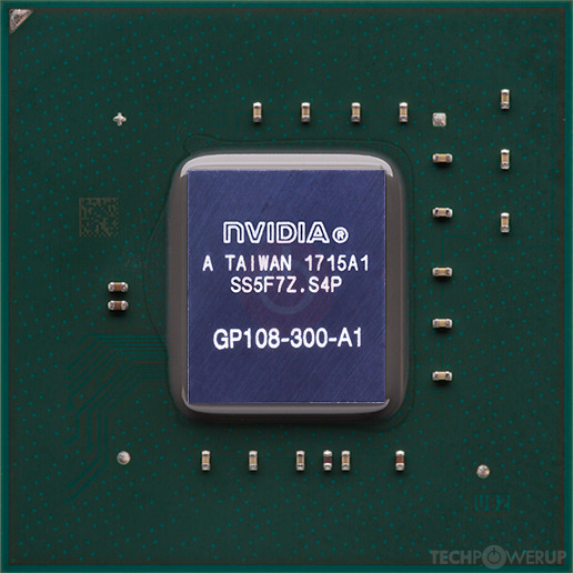
GP108-300-A1

GP108-310-A1

GP108 BGA

Block Diagram
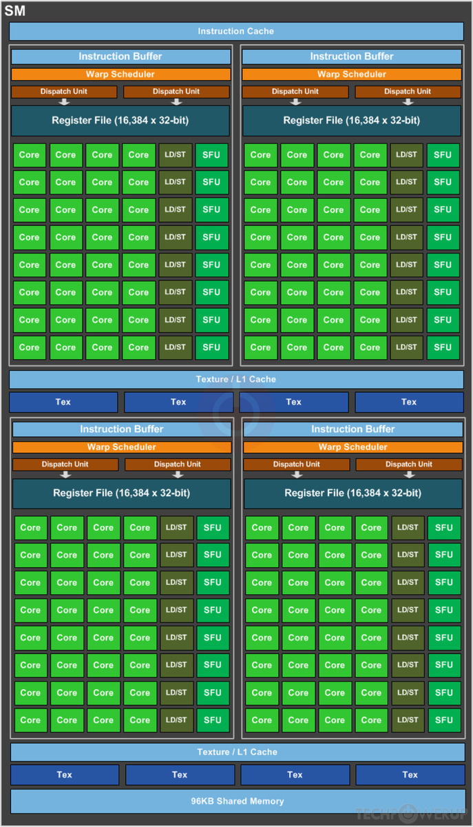
SM Diagram
NVIDIA's GP108 GPU uses the Pascal architecture and is made using a 14 nm production process at Samsung. With a die size of 74 mm² and a transistor count of 1,800 million it is a very small chip. GP108 supports DirectX 12 (Feature Level 12_1). For GPU compute applications, OpenCL version 3.0 and CUDA 6.1 can be used. It features 384 shading units, 24 texture mapping units and 16 ROPs.
Graphics Processor
- Released
- May 17th, 2017
- GPU Name
- GP108
- Codename
- NV138
- Architecture
- Pascal
- Foundry
- Samsung
- Process Size
- 14 nm
- Transistors
- 1,800 million
- Density
- 24.3M / mm²
- Die Size
- 74 mm²
- Package
- FCBGA-595
Graphics Features
- DirectX
- 12 (12_1)
- OpenGL
- 4.6
- OpenCL
- 3.0
- Vulkan
- 1.3
- CUDA
- 6.1
- Shader Model
- 6.7
- WDDM
- 3.1
- NVENC
- No Support
- NVDEC
- 3rd Gen
- PureVideo HD
- VP8
- VDPAU
- Feature Set H
Render Config
- Shading Units
- 384
- TMUs
- 24
- ROPs
- 16
- SM Count
- 3
- SFUs
- 96
- TPCs
- 3
- GPCs
- 1
- L1 Cache
- 48 KB per SM
- L2 Cache
- 512 KB
- Max. TDP
- 30 W
All Pascal GPUs
NVIDIA GPU Architecture History
- 2024 Blackwell
- 2023 Hopper
- 2022-2024 Ada Lovelace
- 2020-2024 Ampere
- 2018-2022 Turing
- 2017-2020 Volta
- 2016-2021 Pascal
- 2014-2019 Maxwell 2.0
- 2014-2017 Maxwell
- 2013-2015 Kepler 2.0
- 2012-2018 Kepler
- 2010-2016 Fermi 2.0
- 2010-2013 VLIW Vec4
- 2010-2016 Fermi
- 2007-2013 Tesla 2.0
- 2006-2010 Tesla
- 2003-2013 Curie
- 2003-2005 Rankine
- 2001-2003 Kelvin
- 1999-2005 Celsius
- 1998-2000 Fahrenheit
Graphics cards using the NVIDIA GP108 GPU
| Name | Chip | Memory | Shaders | TMUs | ROPs | Base Clock | Boost Clock | Memory Clock |
|---|---|---|---|---|---|---|---|---|
| GP108-300-A1 | 2 GB | 384 | 24 | 16 | 1228 MHz | 1468 MHz | 1502 MHz | |
| GP108-650-A1 | 2 GB | 384 | 24 | 16 | 1469 MHz | 1532 MHz | 1502 MHz | |
| N17S-LG-A1 | 2 GB | 384 | 24 | 16 | 937 MHz | 1038 MHz | 1253 MHz | |
| GP108-310-A1 | 2 GB | 384 | 24 | 16 | 1152 MHz | 1379 MHz | 1050 MHz | |
| 2 GB | 256 | 16 | 16 | 1455 MHz | 1519 MHz | 1253 MHz | ||
| N17S-G0-A1 | 2 GB | 256 | 16 | 16 | 1519 MHz | 1531 MHz | 1502 MHz | |
| N17S-G2-A1 | 2 GB | 384 | 24 | 16 | 1519 MHz | 1582 MHz | 1502 MHz | |
| 2 GB | 384 | 24 | 16 | 1303 MHz | 1493 MHz | 1502 MHz | ||
| GP108-200-A1 | 2 GB | 256 | 16 | 8 | 1228 MHz | 1468 MHz | 1502 MHz | |
| GP108-200-A1 | 2 GB | 256 | 16 | 8 | 1152 MHz | 1380 MHz | 1050 MHz | |
| 4 GB | 384 | 24 | 16 | 1303 MHz | 1493 MHz | 1375 MHz |


GP108 GPU Notes
| NVENC: No Support NVDEC: 3rd Gen PureVideo HD: VP8 VDPAU: Feature Set H |
Apr 29th, 2024 09:59 EDT
change timezone
Latest GPU Drivers
New Forum Posts
- Dialing in the overlock on my new 12600kf, matured silicon process showing great results... (9)
- Is it better for zero RPM PSUs to place the fan on top? (12)
- HP Workstations Owners Club (322)
- Does charging protection matter? (31)
- Why MS buying all of these Studios is bad for Gaming (25)
- What's your latest tech purchase? (20388)
- Z790 ACE MAX? (3)
- EK seems to be having major issues (53)
- Graphics cards (6)
- Old high quality PSU, or semi-old mid-quality PSU? (8)
Popular Reviews
- Ugreen NASync DXP4800 Plus Review
- HYTE THICC Q60 240 mm AIO Review
- Upcoming Hardware Launches 2023 (Updated Feb 2024)
- MOONDROP x Crinacle DUSK In-Ear Monitors Review - The Last 5%
- FiiO K19 Desktop DAC/Headphone Amplifier Review
- Thermalright Phantom Spirit 120 EVO Review
- AMD Ryzen 7 7800X3D Review - The Best Gaming CPU
- ASUS Radeon RX 7900 GRE TUF OC Review
- ASUS GeForce RTX 4070 Ti Super TUF Review
- PNY GeForce RTX 4070 Super Verto Review
Controversial News Posts
- Windows 11 Now Officially Adware as Microsoft Embeds Ads in the Start Menu (146)
- Sony PlayStation 5 Pro Specifications Confirmed, Console Arrives Before Holidays (117)
- Intel Statement on Stability Issues: "Motherboard Makers to Blame" (110)
- NVIDIA Points Intel Raptor Lake CPU Users to Get Help from Intel Amid System Instability Issues (106)
- AMD "Strix Halo" Zen 5 Mobile Processor Pictured: Chiplet-based, Uses 256-bit LPDDR5X (103)
- US Government Wants Nuclear Plants to Offload AI Data Center Expansion (98)
- AMD's RDNA 4 GPUs Could Stick with 18 Gbps GDDR6 Memory (96)
- TechPowerUp Hiring: Reviewers Wanted for Motherboards, Laptops, Gaming Handhelds and Prebuilt Desktops (85)