Report an Error


NVIDIA Quadro T1000 Max-Q
- Graphics Processor
- TU117
- Cores
- 896
- TMUs
- 56
- ROPs
- 32
- Memory Size
- 4 GB
- Memory Type
- GDDR5
- Bus Width
- 128 bit
GPU
Recommended Gaming Resolutions:
- 1920x1080
- 2560x1440
- 3840x2160
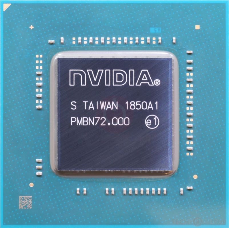
The Quadro T1000 Max-Q is a professional mobile graphics chip by NVIDIA, launched on May 27th, 2019. Built on the 12 nm process, and based on the TU117 graphics processor, the chip supports DirectX 12. The TU117 graphics processor is an average sized chip with a die area of 200 mm² and 4,700 million transistors. It features 896 shading units, 56 texture mapping units, and 32 ROPs. NVIDIA has paired 4 GB GDDR5 memory with the Quadro T1000 Max-Q, which are connected using a 128-bit memory interface. The GPU is operating at a frequency of 765 MHz, which can be boosted up to 1350 MHz, memory is running at 1250 MHz (5 Gbps effective).
Its power draw is rated at 50 W maximum. This device has no display connectivity, as it is not designed to have monitors connected to it. Rather it is intended for use in laptop/notebooks and will use the output of the host mobile device. Quadro T1000 Max-Q is connected to the rest of the system using a PCI-Express 3.0 x16 interface.
Its power draw is rated at 50 W maximum. This device has no display connectivity, as it is not designed to have monitors connected to it. Rather it is intended for use in laptop/notebooks and will use the output of the host mobile device. Quadro T1000 Max-Q is connected to the rest of the system using a PCI-Express 3.0 x16 interface.
Graphics Processor
Mobile Graphics
- Release Date
- May 27th, 2019
- Generation
-
Quadro Turing-M
(Tx000)
- Predecessor
- Quadro Pascal-M
- Successor
- Quadro Ampere-M
- Production
- Active
- Bus Interface
- PCIe 3.0 x16
Relative Performance
Based on TPU review data: "Performance Summary" at 1920x1080, 4K for 2080 Ti and faster.
Performance estimated based on architecture, shader count and clocks.
Clock Speeds
- Base Clock
- 765 MHz
- Boost Clock
- 1350 MHz
- Memory Clock
-
1250 MHz
5 Gbps effective
Memory
- Memory Size
- 4 GB
- Memory Type
- GDDR5
- Memory Bus
- 128 bit
- Bandwidth
- 80.00 GB/s
Render Config
- Shading Units
- 896
- TMUs
- 56
- ROPs
- 32
- SM Count
- 14
- L1 Cache
- 64 KB (per SM)
- L2 Cache
- 1024 KB
Theoretical Performance
- Pixel Rate
- 43.20 GPixel/s
- Texture Rate
- 75.60 GTexel/s
- FP16 (half)
- 4.838 TFLOPS (2:1)
- FP32 (float)
- 2.419 TFLOPS
- FP64 (double)
- 75.60 GFLOPS (1:32)
Board Design
- Slot Width
- IGP
- TDP
- 50 W
- Outputs
- Portable Device Dependent
- Power Connectors
- None
- Board Number
- E4904 SKU 10
Graphics Features
- DirectX
- 12 (12_1)
- OpenGL
- 4.6
- OpenCL
- 3.0
- Vulkan
- 1.3
- CUDA
- 7.5
- Shader Model
- 6.7
TU117 GPU Notes
| NVENC: 5th Gen NVDEC: 4th Gen PureVideo HD: VP10 VDPAU: Feature Set J |
Devices based on this design (1)
| Name | GPU Clock | Boost Clock | Memory Clock | Other Changes |
|---|---|---|---|---|
| 1155 MHz | 1500 MHz | 1250 MHz | GDDR6 |
May 3rd, 2024 11:04 EDT
change timezone
Latest GPU Drivers
New Forum Posts
- TPU's Nostalgic Hardware Club (18494)
- Is this Sapphire PULSE RX 5600 XT legit or fake? (32)
- My Laptop is having issues with PL2 and EDP OTHER (1)
- Strange system crashes out of nowhere, help (23)
- Which PSU to take? (47)
- 7900 XTX Seriously lacking (108)
- FINAL FANTASY XIV: Dawntrail Official Benchmark (78)
- Just for lolz, Post your 3DMark2001SE Benchmark scores! (86)
- Ryzen Owners Zen Garden (7292)
- Your PC ATM (34542)
Popular Reviews
- HYTE THICC Q60 240 mm AIO Review
- ASRock NUC BOX-155H (Intel Core Ultra 7 155H) Review
- Meze Audio LIRIC 2nd Generation Closed-Back Headphones Review
- Montech Sky Two GX Review
- Ugreen NASync DXP4800 Plus Review
- Upcoming Hardware Launches 2023 (Updated Feb 2024)
- Team Group T-Force Vulcan ECO DDR5-6000 32 GB CL38 Review
- MOONDROP x Crinacle DUSK In-Ear Monitors Review - The Last 5%
- AMD Ryzen 7 7800X3D Review - The Best Gaming CPU
- Logitech G Pro X Superlight 2 Review - Updated with 4000 Hz Tested
Controversial News Posts
- Intel Statement on Stability Issues: "Motherboard Makers to Blame" (233)
- Windows 11 Now Officially Adware as Microsoft Embeds Ads in the Start Menu (167)
- Sony PlayStation 5 Pro Specifications Confirmed, Console Arrives Before Holidays (117)
- AMD's RDNA 4 GPUs Could Stick with 18 Gbps GDDR6 Memory (114)
- NVIDIA Points Intel Raptor Lake CPU Users to Get Help from Intel Amid System Instability Issues (106)
- AMD "Strix Halo" Zen 5 Mobile Processor Pictured: Chiplet-based, Uses 256-bit LPDDR5X (103)
- AMD Ryzen 9 7900X3D Now at a Mouth-watering $329 (103)
- TechPowerUp Hiring: Reviewers Wanted for Motherboards, Laptops, Gaming Handhelds and Prebuilt Desktops (93)