Report an Error


ATI Radeon HD 3650
- Graphics Processor
- RV635
- Cores
- 120
- TMUs
- 8
- ROPs
- 4
- Memory Size
- 256 MB
- Memory Type
- GDDR3
- Bus Width
- 128 bit

GPU

I/O
Recommended Gaming Resolutions:
- 640x480
- 1280x720
- 1366x768
The Radeon HD 3650 was a graphics card by ATI, launched on January 20th, 2008. Built on the 55 nm process, and based on the RV635 graphics processor, in its RV635 PRO variant, the card supports DirectX 10.1. Since Radeon HD 3650 does not support DirectX 11 or DirectX 12, it might not be able to run all the latest games. The RV635 graphics processor is an average sized chip with a die area of 135 mm² and 378 million transistors. It features 120 shading units, 8 texture mapping units, and 4 ROPs. ATI has paired 256 MB GDDR3 memory with the Radeon HD 3650, which are connected using a 128-bit memory interface. The GPU is operating at a frequency of 725 MHz, memory is running at 800 MHz.
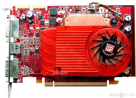
Being a single-slot card, the ATI Radeon HD 3650 does not require any additional power connector, its power draw is rated at 65 W maximum. Display outputs include: 2x DVI, 1x S-Video. Radeon HD 3650 is connected to the rest of the system using a PCI-Express 2.0 x16 interface.
Being a single-slot card, the ATI Radeon HD 3650 does not require any additional power connector, its power draw is rated at 65 W maximum. Display outputs include: 2x DVI, 1x S-Video. Radeon HD 3650 is connected to the rest of the system using a PCI-Express 2.0 x16 interface.
Graphics Processor
Graphics Card
- Release Date
- Jan 20th, 2008
- Generation
-
Radeon R600
(HD 3600)
- Predecessor
- Radeon R500 PCIe
- Successor
- Radeon R700
- Production
- End-of-life
- Bus Interface
- PCIe 2.0 x16
- Reviews
- 28 in our database
Relative Performance
Based on TPU review data: "Performance Summary" at 1920x1080, 4K for 2080 Ti and faster.
Performance estimated based on architecture, shader count and clocks.
Clock Speeds
- GPU Clock
- 725 MHz
- Memory Clock
-
800 MHz
1600 Mbps effective
Memory
- Memory Size
- 256 MB
- Memory Type
- GDDR3
- Memory Bus
- 128 bit
- Bandwidth
- 25.60 GB/s
Render Config
- Shading Units
- 120
- TMUs
- 8
- ROPs
- 4
- Compute Units
- 3
- L2 Cache
- 128 KB
Theoretical Performance
- Pixel Rate
- 2.900 GPixel/s
- Texture Rate
- 5.800 GTexel/s
- FP32 (float)
- 174.0 GFLOPS
Board Design
- Slot Width
- Single-slot
- TDP
- 65 W
- Suggested PSU
- 250 W
- Outputs
- 2x DVI
1x S-Video
- Power Connectors
- None
- Board Number
- 109-B381,
109-B38231-10
Graphics Features
- DirectX
- 10.1 (10_1)
- OpenGL
- 3.3
- OpenCL
- N/A
- Vulkan
- N/A
- Shader Model
- 4.1
RV635 GPU Notes
| Mobile Variant: M86 Codename: Wario Graphics/Compute: GFX3 Display Core Engine: 3.0 Unified Video Decoder: 1.0 |
Retail boards based on this design (11)
| Name | GPU Clock | Memory Clock | Other Changes |
|---|---|---|---|
| 725 MHz | 400 MHz | 1024 MB, DDR2, Dual-slot | |
| 725 MHz | 700 MHz | 512 MB, Dual-slot | |
| 800 MHz | 900 MHz | ||
| 725 MHz | 800 MHz | 1x DVI 1x HDMI 1x DisplayPort | |
| 725 MHz | 400 MHz | 1024 MB, DDR2 | |
| 800 MHz | 900 MHz | 512 MB | |
| 725 MHz | 400 MHz | DDR2 | |
| 725 MHz | 400 MHz | 1024 MB, DDR2, 1x DVI 1x VGA | |
| 725 MHz | 400 MHz | 512 MB, DDR2 | |
| 725 MHz | 400 MHz | 512 MB, DDR2 | |
| 725 MHz | 400 MHz | 1024 MB, DDR2 |


May 9th, 2024 12:13 EDT
change timezone
Latest GPU Drivers
New Forum Posts
- Microsoft butchering Xbox Studios (24)
- What's a good option for a digital touchless thermometer? (16)
- Dell Workstation Owners Club (3068)
- What are you playing? (20604)
- Last game you purchased? (272)
- Your way of cooling your PC? (85)
- Soundblaster x-ae5 plus sometimes switches center channel to other channels. (1)
- Share your AIDA 64 cache and memory benchmark here (2933)
- Scratches on the processor. How critical is it? (7)
- 6800XT Red Devil with 18°C difference from Core to Hotspot (10)
Popular Reviews
- CHERRY XTRFY M64 Pro Review
- Corsair iCUE Link RX120 RGB 120 mm Fan Review
- Bykski CPU-XPR-C-I CPU Water Block Review - Amazing Value!
- Finalmouse UltralightX Review
- Upcoming Hardware Launches 2023 (Updated Feb 2024)
- AMD Ryzen 7 7800X3D Review - The Best Gaming CPU
- Cougar Hotrod Royal Gaming Chair Review
- Meze Audio LIRIC 2nd Generation Closed-Back Headphones Review
- ASUS Radeon RX 7900 GRE TUF OC Review
- ASRock NUC BOX-155H (Intel Core Ultra 7 155H) Review
Controversial News Posts
- Intel Statement on Stability Issues: "Motherboard Makers to Blame" (262)
- AMD to Redesign Ray Tracing Hardware on RDNA 4 (206)
- Windows 11 Now Officially Adware as Microsoft Embeds Ads in the Start Menu (167)
- NVIDIA to Only Launch the Flagship GeForce RTX 5090 in 2024, Rest of the Series in 2025 (144)
- Sony PlayStation 5 Pro Specifications Confirmed, Console Arrives Before Holidays (119)
- AMD's RDNA 4 GPUs Could Stick with 18 Gbps GDDR6 Memory (114)
- NVIDIA Points Intel Raptor Lake CPU Users to Get Help from Intel Amid System Instability Issues (106)
- AMD Ryzen 9 7900X3D Now at a Mouth-watering $329 (104)