News Posts matching #Cannon Lake

Return to Keyword Browsing

Intel's Manufacturing Outlook for the Future Doesn't Inspire Confidence in Successful Competition, According to Susquehanna Call

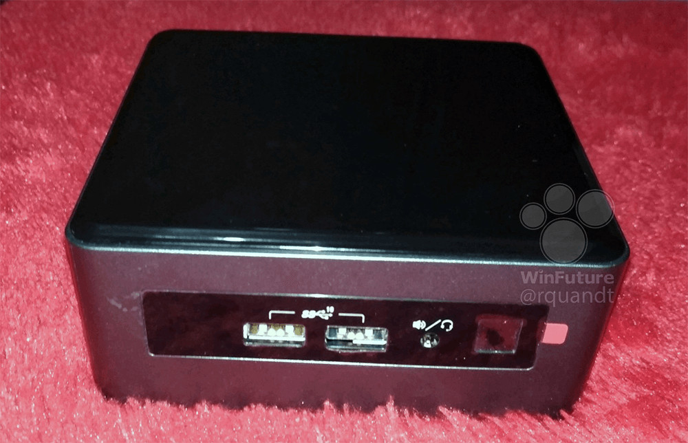
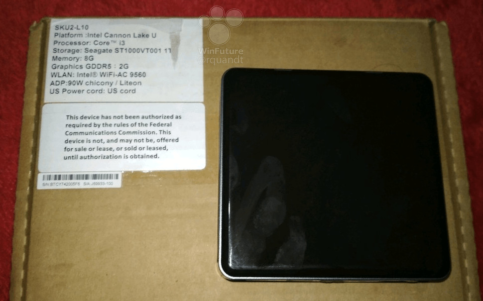
Susquehanna is a global trading firm which has various interests in silicon manufacturing - and part of that interest is naturally materialized in Intel. In a recent group call from the firm, some details on Intel's manufacturing and product design woes came to light, which point towards even more execution slips than we've already seen. During the call, a number of points were broached, including dismal yields for Intel's 10 nm manufacturing process as of its introduction in late 2018 (which is why it never saw mainstream adoption from the company). News that Intel is looking for a new CEO also don't instill confidence on current CEO Bob Swan's capacity to steer the Intel behemoth.

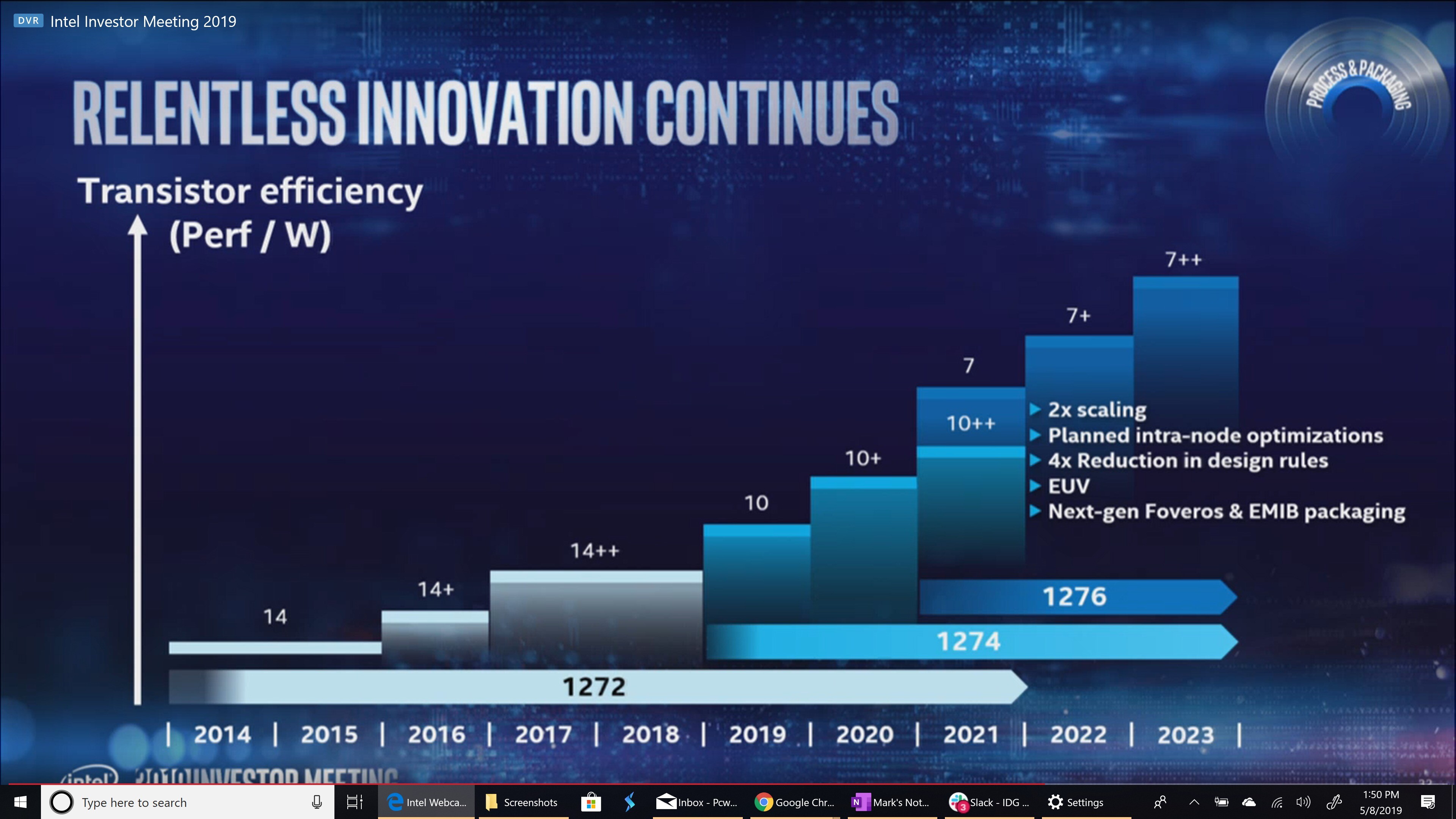
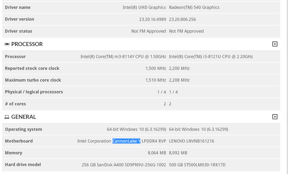
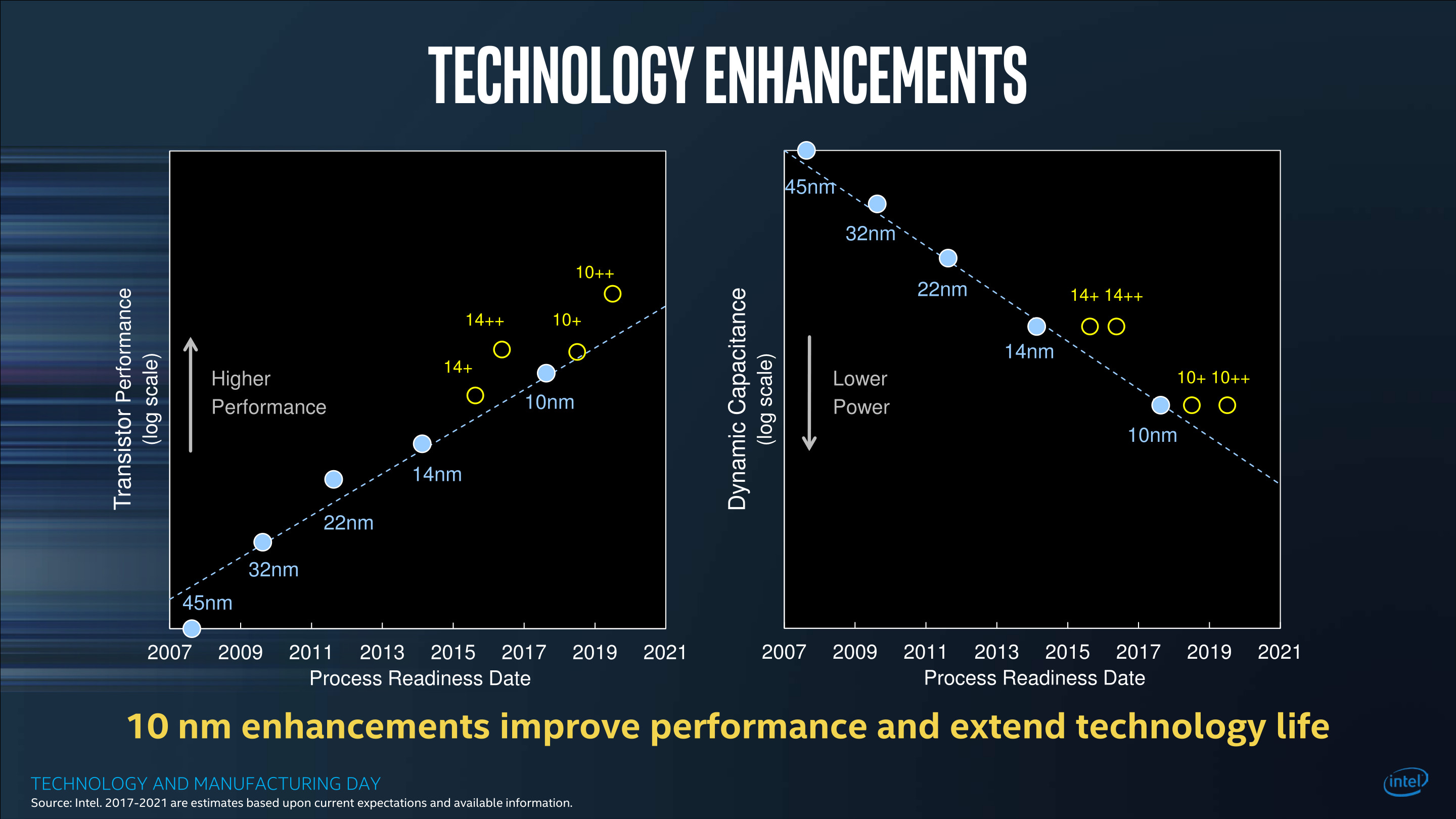
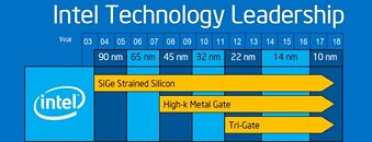
Improved yields on 10 nm are being reported due to deployment of Intel's SuperFin technology, which improved yields to upwards of 50%, but still keeps them under the ones achieved in Intel's 14 nm process; an eye-opening tidbit in that Cannon Lake on 10 nm originally saw yields of only 25% usable chips per wafer; and that backporting Rocket Lake meant Intel had to deal with unfathomably large chips and high power consumption characteristics. And to add insult to injury, there is still not a definite timetable for 7 nm deployment, with delays being expected to be worse than the previously reported 6-12 months. This all paints a somewhat grim picture for Intel's capacity to compete with TSMC-powered AMD in many of its most important markets; the blue giant won't topple, of course, but it's expected that five years from now, we'll be looking at a very different outlook in the market between AMD and Intel. You can check the talked-about points in the call via the transcript after the break. You should still take the transcript with a grain of salt.

AMD Ryzen 9 3000 is a 16-core Socket AM4 Beast

AMD is giving finishing touches to its 3rd generation Ryzen socket AM4 processor family which is slated for a Computex 2019 unveiling, followed by a possible E3 market availability. Based on the "Matisse" multi-chip module that combines up to two 8-core "Zen 2" chiplets with a 14 nm I/O controller die, these processors see a 50-100 percent increase in core-counts over the current generation. The Ryzen 5 series now includes 8-core/16-thread parts, the Ryzen 7 series chips are 12-core/24-thread, while the newly created Ryzen 9 series (designed to rival Intel Core i9 LGA115x), will include 16-core/32-thread chips.

Thai PC enthusiast TUM_APISAK confirmed the existence of the Ryzen 9 series having landed himself with an engineering sample of the 16-core/32-thread chip that ticks at 3.30 GHz with 4.30 GHz Precision Boost frequency. The infamous Adored TV leaks that drew the skeleton of AMD's 3rd generation Ryzen roadmap, referenced two desktop Ryzen 9 parts, the Ryzen 9 3800X and Ryzen 9 3850X. The 3800X is supposed to be clocked at 3.90 GHz with 4.70 GHz boost, with a TDP rating of 125W, while the 3850X tops the charts at 4.30 GHz base and a staggering 5.10 GHz boost. The rated TDP has shot up to 135W. We can now imagine why some motherboard vendors are selective with BIOS updates on some of their lower-end boards. AMD is probably maximizing the clock-speed headroom of these chips out of the box, to preempt Intel's "Comet Lake" 10-core/20-thread processor.

Intel Readies Crimson Canyon NUC with 10nm Core i3 and AMD Radeon

Intel is giving final touches to a "Crimson Canyon" fully-assembled NUC desktop model which combines the company's first 10 nm Core processor, and AMD Radeon discrete graphics. The NUC8i3CYSM desktop from Intel packs a Core i3-8121U "Cannon Lake" SoC, 8 GB of dual-channel LPDDR4 memory, and discrete AMD Radeon RX 540 mobile GPU with 2 GB of dedicated GDDR5 memory. A 1 TB 2.5-inch hard drive comes included, although you also get an M.2-2280 slot with both PCIe 3.0 x4 (NVMe) and SATA 6 Gbps wiring. The i3-8121U packs a 2-core/4-thread CPU clocked up to 3.20 GHz and 4 MB of L3 cache; while the RX 540 packs 512 stream processors based on the "Polaris" architecture.

The NUC8i3CYSM offers plenty of modern connectivity, including 802.11ac + Bluetooth 5.0 powered by an Intel Wireless-AC 9560 WLAN card, wired 1 GbE from an Intel i219-V controller, consumer IR receiver, an included beam-forming microphone, an SDXC card reader, and stereo HD audio. USB connectivity includes four USB 3.1 type-A ports including a high-current port. Display outputs are care of two HDMI 2.0b, each with 7.1-channel digital audio passthrough. The company didn't reveal pricing, although you can already read a performance review of this NUC from the source link below.

Intel "Crimson Canyon" NUCs with Discrete GPUs Up for Pre-order

One of the first Intel NUC (next unit of computing) mini PCs to feature completely discrete GPUs (and not MCMs of CPUs and GPUs), the "Crimson Canyon" NUC8i3CYSM and NUC8i3CYSN, are up for pre-order. The former is priced at USD $529, while the latter goes for $574. The two combine Intel's 10 nm Core i3-8121U "Cannon Lake" SoC with AMD Radeon 540 discrete GPU. Unlike the "Hades Canyon" NUC, which features an MCM with a powerful AMD Radeon Vega M GPU die and a quad-core "Kaby Lake" CPU die; the "Crimson Canyon" features its processor and GPU on separate packages. The Radeon 540 packs 512 stream processors, 32 TMUs, and 16 ROPs; with 2 GB of GDDR5 memory.

All that's differentiating the NUC8i3CYSM from the NUC8i3CYSN is memory. You get 4 GB of LPDDR4 memory with the former, and 8 GB of it with the latter. Both units come with a 2.5-inch 1 TB HDD pre-installed. You also get an M.2-2280 slot with PCIe 3.0 x4 wiring, and support for Optane caching. Intel Wireless-AC 9560 WLAN card handles wireless networking, while an i219-V handles wired. Connectivity includes four USB 3.0 type-A ports, one of which has high current; an SDXC card reader, CIR, two HDMI 2.0 outputs, and 7.1-channel HD audio. The NUC has certainly grown in size over the years. This one measures 117 mm x 112 mm x 52 mm (WxDxH). An external 90W power-brick adds to the bulk.

Intel Core M3 8114Y "Cannon Lake-Y" Processor Surfaces in 3DMark

The Intel Core i3-8121U was the first Cannon Lake processor to be revealed to the public. Today, we got word of the existence of another 10 nm chip. The Intel Core M3 8114Y, as its name implies, belongs to the low-powered Cannon Lake-Y family. It's a dual-core processor with four threads that runs at a base clock of 1.5 GHz. Although there was no mention of the processor's boost clocks, the Core M3 8114Y is expected to boost to 2.2 GHz. Like its predecessor, the chip should have a 4.5 W TDP. The 3DMark results also revealed that this model in particular supports LPDDR4 memory. Unlike the Core i3-8121U which has its iGPU disabled, the Core M3 8114Y comes with an Intel UHD Graphics iGPU.

Intel "Cannon Lake" Confirmed to Feature AVX-512 Instruction-Set

Intel updated the ARK information page for its stealthily launched 10 nm production chip, the Core i3-8121U "Cannon Lake," to confirm that the chip supports the new AVX-512 instruction-set. This is the first "mainstream" client-segment processor by the company to feature the extremely advanced instruction-set that, if implemented properly on the software side, can double performance/Watt compared to tasks that can take advantage of AVX2.

The instruction-set made its debut with the Xeon Phi "Knights Landing" HPC processor, and made its client-segment debut with the Core X "Skylake X" HEDT processors. It remains to be seen if the implementation of AVX-512 on "Cannon Lake" is complete, or if some instructions found on HPC processors such as the Xeon Phi are omitted due to irrelevance to the client platform.

Intel Core i3-8121U "Cannon Lake" Processor Debuts in Lenovo Ideapad 330 Laptop

Online Chinese retailer JD.com has listed Lenovo's latest Cannon Lake-based Ideapad 330 laptop on its website. The Ideapad 330 incorporates an Intel Core i3-8121U dual-core processor fabricated on Intel's 10 nm process. The processor comes with a base frequency of 2.2 GHz and lacks integrated graphics as it's been disabled. Therefore, Lenovo pairs the Intel Core i3-8121U processor with an AMD Radeon RX 540 2GB graphics card in this particular laptop. The base model is equipped with 4 GB of DDR4-2400 memory and a 500 GB 5400RPM hard drive. However, JD.com also offers numerous configurations including one with 8 GB of memory, 256 GB SSD and 1 TB hard drive.

The 15.6-inch Ideapad 330 uses a TN panel with a resolution of 1366 x 768 pixels. The laptop measures 378 x 260 x 22.7 mm and weights approximately 2.1 kg. According to JD.com, the battery life is estimated to around five hours. Connectivity options include a Gigabit Ethernet port, two USB 3.0 Type-A ports, a single USB Type-C port, a 3.5mm jack, a HDMI port, and a CD/DVD drive. The base model costs 3299 CNY (~$445) while the highest-end model will set you back 4299 CNY (~$580).

Intel Confirms Z390 and X399 Chipsets in Official Documents

Intel unintentionally confirmed the existence of two of its upcoming client platform chipsets, the Z390 Express, and the X399 Express. The latest release-notes documentation of its Rapid Storage Technology driver, mentions Z390 and X399, alongside the CPU micro-architectures they support. The Z390 supports current-generation "Coffee Lake" and upcoming "Cannon Lake" processors, while the X399 supports HEDT derivatives based on the two architectures, namely "Coffee Lake-X" and "Cannon Lake-X," with no mention of "Skylake-X."

What happens to the X299, you ask? The table mentions the chipset as supporting SKL-X (Skylake-X) and KBL-X (Kaby Lake-X), but it's not clear if Intel is only referring to the forgettable i7-7740X and i5-7640X with "KBL-X." The Z390 is rumored as being Intel's next top mainstream-desktop chipset, with a long overdue update to onboard audio standards, in being a departure from the "Azalia" HD audio specification, onward to the new Programmable Quad-Core Audio with new SoundWire digital audio interface. The chipset is also rumored to feature 10 Gbps USB 3.1 ports.

Intel Crimson Canyon NUC to Feature Cannon Lake-U CPU and Radeon 500 Graphics

Photographs of Intel's Crimson Canyon NUC have finally surfaced. WinFuture managed to get their hands on one that's powered by an Intel Core i3-8121U dual-core processor based on the Cannon Lake architecture. The NUCs come with 4 GB or 8 GB of memory, a 2.5-inch hard drive, built-in Wi-Fi 802.11ac, and Bluetooth 5.0 connectivity. The Crimson Canyon NUC also features a discrete AMD Radeon graphics card. The "Radeon 500-series" reference in one of the screenshots along with the "2GB of GDDR5" on the packaging takes us to the conclusion that Intel is most likely integrating a Polaris-based graphics card into the Crimson Canyon NUC. It's highly unlikely that we will find the CPU and GPU on the same chip like the one in the Hades Canyon NUC. Instead, the GPU will probably be soldered directly to the motherboard itself. The Intel Core i3-8121U models (NUC8I3CYSM2 and NUC8I3CYSM3) start around 450 euros, which roughly translates to $550. There was no mention when they will be available though.

Intel Could Develop its own big.LITTLE x86 Adaptation

big.LITTLE is an innovation by ARM, which seeks to minimize power-draw on mobile devices. It is a sort of heterogeneous multi-core CPU design, in which a few "big" high-performance CPU cores work alongside a few extremely low-power "little" CPU cores. The idea here is that the low-power cores consume much lesser power at max load, than the high-performance cores at their minimum power-state, so the high-performance cores can be power-gated when the system doesn't need them (i.e. most of the time).

Intel finds itself with two distinct x86 implementations at any given time. It has low-power CPU micro-architectures such as "Silvermont," "Goldmont," and "Goldmont Plus," etc., implemented on low-power product lines such as the Pentium Silver series; and it has high-performance micro-architectures, such as "Haswell," "Skylake," and "Coffee Lake." The company wants to take a swing at its own heterogeneous multi-core CPU, according to tech stock analyst Ashraf Eassa, with the Motley Fool.

Intel 10 nm CPUs to See Very Limited Initial Launch in 2017

UPDATE: Some slides have surfaced today on Reddit that actually place Intel's updated 10 nm roadmap as starting initial risk production in 2Q 2018. The same leaks also point towards a yearly advancement in process technology (akin to Intel's current 14 nm+ and 14 nm++ production processes), with 10 nm+ risk production on 1Q 2019 and 10 nm++ on 1Q 2020. This roadmap, however, is relative to Intel's Custom Foundry partners; as such, this doesn't go directly against Intel CEO's Brian Kzarnich remarks on the latest investor call, since he was likely talking about the 10 nm ramp-up on Intel's own products.

Intel CEO Brian Krzanich has come out to say that the company's first 10 nm CPUs based on the "Cannon Lake" micro-architecture will see the light of day before this year's end. Intel has been having a slew of ramp-up delays with its 10 nm products, which prompted a slippage from an expected 2016, full-scale launch (whose ship has sailed, clearly) towards a timed, product-tier based strategy. Intel opted to first introduce 10 nm technology to FPGA accelerators, which due to their redundancy, would suffer less from yield issues.

Intel "Cannon Lake" Could Bring AVX-512 Instruction-set to the Mainstream

Intel's next-generation "Cannon Lake" CPU micro-architecture could see the introduction of the AVX-512 instruction-set to the mainstream segments (MSDT or mainstream-desktop, and mobile). It is currently available on the company's Core X "Skylake-X" HEDT processors, and on the company's Xeon "Skylake-W," Xeon Scalable "Skylake-SP," and in a limited form on the Xeon Phi Knights Landing and Knights Mill scalar compute chips.

The upcoming "Cannon Lake" mainstream silicon will feature AVX512F, AVX512CD, AVX512DQ, AVX512BW, and AVX512VL instructions, and will support AVX512_IFMA and AVX512_VBMI commands, making it a slightly broader implementation of AVX-512 than the "Skylake-SP" silicon. The new AVX-512 will vastly improve performance of compute-intensive applications that take advantage of it. It will also be a key component of future security standards.

Intel "Sapphire Rapids" Micro-architecture Succeeds "Tiger Lake"

Intel revealed the very first hint at its post-"Ice Lake"/"Tiger Lake" processor lineup, which will likely be built on the company's 7 nanometer silicon fab process. Its 12th generation Core processor will be built on the new "Sapphire Rapids" silicon, which will be a major micro-architecture change, and could put 8-core into more hands. The processor, along with its companion chipset, will make up the "Tinsley" platform, which is expected to hit the market in 2020.

Following its 8th generation Core "Coffee Lake" lineup, Intel could built 2-3 micro-architectures on its new 10 nm process, namely "Cannon Lake," "Ice Lake," and "Tiger Lake," which could be released over the next three years. "Sapphire Rapids" could be launched on the process that succeeds 10 nm, likely 7 nm, with a launch timeline likely around 2020.

Intel Delays 10nm "Cannon Lake" to Late-2018

Intel is reportedly delaying the roll-out of its first processors built on its 10 nanometer silicon fabrication process, codenamed "Cannon Lake" for the third time since its inception. The first products based on the silicon will now come out only by late-2018. In the meantime, Intel could continue to ride on its new 8th generation Core "Coffee Lake" processors, including the augmentation of an 8-core mainstream desktop (MSDT) part in the second-half of 2018.

Notebook manufacturers are less than enthusiastic about "Cannon Lake," and plan to skip it altogether for its successor, codenamed "Ice Lake," which could come out in 2019. It won't be the first time OEMs have done this, as Intel's 5th generation Core "Broadwell" architecture was mostly skipped over in the notebook and MSDT segments.

Intel Officially Reveals What's Coming After Coffee Lake: The 10 nm Ice Lake

A pretty underwhelming post on Intel's official page has pulled the curtains of the company's architecture name post their 8th generation processors. Actually, it's a little more puzzling than that, since Intel is actually detailing the codename of an architecture that's supposed to come right after their 8th generation - read, Coffee Lake - processors. Keep in mind that Coffee Lake, whilst being supposed to bring a reorganization of Intel's product stack in response to AMD's Ryzen success, will still be in the 14 nm++ process - the third such architecture in the same process, after Skylake (14 nm) and Kaby Lake (14 nm+) before it. Cannon Lake, however, is supposed to be the company's first tick into the 10 nm process.

Intel has moved over from their famed tick-tock (where tick is a process shrink and tock is a new architecture on the same process) cadence, and are now telling customers to expect at least three "tocks" per process. It's expected that Intel will launch mobile processors on the 10 nm process before any desktop parts are launched on the same process; this could stem from the fact that mobile parts are typically lower-power, smaller-sized dies, which are easier and cheaper to produce out of a still maturing 10 nm process, which usually implies lower than ideal yields.
Return to Keyword Browsing
Apr 25th, 2024 23:56 EDT change timezone

New Forum Posts

Popular Reviews

Controversial News Posts