News Posts matching #LPDDR6

Return to Keyword Browsing

Axelera AI Unveils Titania Architecture

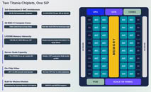
Axelera AI, the leading provider of purpose-built AI hardware acceleration technology, unveiled the details behind Titania, its third-generation silicon architecture in a chiplet design. Titania is highly programmable and energy efficient and will deliver high performance at interactive speeds, all within the power and cooling limits of existing data centers, rather than the 100-kilowatt-plus liquid-cooled racks that today's highest-density GPU systems require.

Performance expectations for Titania are up to 7x the throughput per watt compared to the best data center grade servers available, and up to a 20x better TCO. Each Titania-based system-in-package (SiP) will contain two Titania chiplets which are then packaged in a range of form factors, including standard PCIe cards as well as OCP-compliant UBB baseboards with eight Titania OAM modules connected in a scale-up network. In support of over $300 million in confirmed Titania commitments, these form factors will be available via OEM partners in an inference server configuration in both air- and liquid-cooled configurations.

Intel "Razor Lake-AX" to Pack 700 TOPS of AI Compute

Intel's senior vice president, Cho Min-sung, announced at the Semiconductors Powering Humanoids summit in South Korea that the next-generation "Razor Lake-AX" platform will be a computing powerhouse, featuring 700 TOPS of AI compute on die. This means that at INT8/FP8 precision, "Razor Lake-AX" will outperform the current "Panther Lake" mobile chips by 3.88 times, which have a total compute power of 180 TOPS. This represents a significant boost in compute power for the SoC, primarily derived from a large integrated GPU alongside a substantial CPU complex. Earlier reports indicated that the "Razor Lake-AX" iGPU will be available in two versions: one with a 16-core iGPU and a flagship SKU with a 32-core iGPU.

Both of these integrated graphics solutions are expected to be based on Intel's Xe3 graphics IP, currently found in "Panther Lake." This would make "Razor Lake-AX" nearly three times as powerful as the current Arc B390, which powers Intel's PTL lineup. This suggests that "Razor Lake-AX" will be a large package, as the GPU die is reportedly around 162.84 mm². We also learned that Intel plans to reintroduce on-package memory with the upcoming "AX" chip. Although the company initially stated that the Core Ultra 200V "Lunar Lake" was the last design with on-package memory, Intel is reportedly bringing back on-package LPDDR5X/LPDDR6 memory for "Razor Lake-AX." Do note that the image below is simply an illustration.

Rambus Advances Power-Efficient AI Infrastructure with Industry-Leading PMIC Designed for LPDDR6 SOCAMM2

Rambus Inc., a premier chip and silicon IP provider making data faster and safer, today announced an industry-leading Power Management IC (PMIC) designed to enable low-power, high-performance LPDDR6 Small Outline Compression Attached Memory Modules (SOCAMM2). Developed in technical cooperation with customers and ecosystem partners to support future-generation accelerated AI infrastructure, the PMIC expands the Rambus family of LPDDR-based server module chips and extends Rambus leadership in advanced server memory products.

As AI training and inference workloads scale, the need for higher throughput within a given power envelope, measured in tokens per watt, is a critical consideration for AI infrastructure. This is driving demand for purpose-built memory solutions optimized for power efficiency, form factor and scalability. SOCAMM2 brings the power and performance benefits of LPDDR technology to a compact, modular and serviceable server-memory architecture designed for demanding AI systems. LPDDR6 SOCAMM2, in development now, represents the next important evolution in LPDDR-based server memory technology.

SK hynix Boosts Leading-Edge 1c DRAM Production to a Dominant Position

SK hynix is shifting much of its capacity to the latest 1c DRAM node, according to recent reports. The South Korean giant is transitioning the bulk of its memory production between nodes, and as DRAM technology advances, the company is moving its production to more advanced 10 nm-class nodes. For SK hynix, the sixth-generation 10 nm class 1c DRAM node accounted for 10% of production in Q1 2026, with an increase to about 13% in Q2. In the current third quarter, the company is expected to manufacture 24% of its DRAM on 1c, while Q4 will see more than a third (34%) produced on that node. By Q1 2027, the 1c node will account for around 35%, making the fifth-generation 10 nm-class 1b node at 33%, officially SK hynix's most dominant node.

As a reminder, DRAM nodes are not the same as conventional logic nodes. DRAM manufacturers use variations of 10 nm and scale them with more EUV layers or advanced features. For SK hynix, the currently dominant 1b node is around 12-13 nm in actual design and involves about 4 layers of EUV patterning, while the most advanced 1c node shrinks to 11-12 nm with 5-6 layers of EUV. SK hynix will use the 1c node to manufacture HBM4E, LPDDR6, and DDR5 memory. For the older 1b node, SK hynix produces DDR5, LPDDR5X, HBM3E, and HBM4.

CXMT Officially Starts Mass Production of LPDDR6 Memory

CXMT has achieved the remarkable feat of officially beginning high-volume manufacturing of LPDDR6 memory. This positions CXMT's LPDDR6 memory modules as some of the first in the industry, with South Korean memory makers on a similar timeline for volume production of this next-generation technology. Reportedly, Xiaomi is the first customer for CXMT's domestic LPDDR6 memory, set to feature in the upcoming Xiaomi 18 Fold smartphone. Since the Xiaomi 18 Fold is scheduled to launch in September, CXMT's LPDDR6 memory will need to be delivered before the end of the month, indicating that customer shipments are already underway. This news follows recent reports that CXMT is conducting risk production of LPDDR6, suggesting a very high yield in production.

CXMT's LPDDR6 memory will operate at speeds of up to 12.8 Gbps, with the base speed of LPDDR6 being 10.7 Gbps. LPDDR6 builds on where LPDDR5X left off, which could reach speeds of up to 10.7 Gbps when highly overclocked. However, the new standard aims for significantly higher speeds, with the first generation of LPDDR6 from CXMT's fabs reaching 12.8 Gbps. Additionally, CXMT is producing these chips with a 16 Gb capacity, equivalent to 2 GB, and the memory IC is housed in a package-on-package (POP) casing, featuring about 1,295 pins in a ball grid array.
Update, 14:55 UTC, September 7th : CXMT's official website confirmed mass production, with Alibaba Cloud, ByteDance, Tencent, Lenovo, Transsion, Honor, Vivo, and Oppo as customers.

Possible AMD RDNA 5 GPU IP Ships Inside a Samsung SoC on 2 nm Node

Today marks the day we see AMD's next-generation RDNA 5 GPU IP inside working silicon, but not in the form you might expect. Thanks to SemiAnalysis's die annotation of the Exynos 2700 SoC from Samsung, we see AMD's new GPU IP shine in a mobile form with the Xclipse 970 GPU. As earlier leaks reported, AMD and Samsung co-developed the Xclipse 970 GPU using AMD RDNA technology and adapted it for mobile. However, the GPU IP has now been upgraded to the latest RDNA 5, making this SoC technically the first RDNA 5-equipped chip that will be shipping. Built on Samsung Foundry's SF2 node, Samsung has designed this SoC with a unique 10-CPU core configuration and a strong GPU to compete with Qualcomm Snapdragon Elite SoCs.

On the CPU front, Samsung uses Arm's off-the-shelf CPU core IP, which includes C2-Ultra and C2-Pro. This setup features a single C2-Ultra big core running at 4.24 GHz, one C2-Ultra running at 3.36 GHz, four C2-Pro cores running at 3.74 GHz, and four C2-Pro cores running at 2.88 GHz, making a total of 10 CPU cores. On the GPU side, the Xclipse 970 packs eight GPU WGPs, each containing two Compute Units. This results in 16 CUs on the GPU front if everything remains the same with RDNA 5 and no changes to the WGP/CU ratio have been made by AMD since the last-generation RDNA 4.

Micron Explores Near-GPU NAND Flash to Run Bigger LLMs

Micron is reportedly exploring the idea of developing high-endurance NAND Flash modules that would be positioned closer to the GPU, rather than being located far away in the storage pool behind multiple protocols. The company is said to be investigating ways to bring NAND Flash closer to handle workloads that don't require the latency and bandwidth of traditional HBM or regular DRAM modules. This architecture, currently referred to as "near-GPU NAND," would serve as a middle ground between density and durability. This concept would allow GPUs to access a pool of NAND Flash that has a lower density than conventional TLC or QLC NAND, but instead focuses on improving I/O speeds, bandwidth, and read times.

For instance, this would enable a GPU to access a potential storage pool with hundreds of gigabytes of storage directly on the GPU package or PCB, similar to what DRAM like HBM or GDDR7/LPDDR6 already does. This tier would sit between GPU memory and regular system storage, acting as a very fast buffer, which would be ideal for the inference of massive LLMs. At that point, LLMs wouldn't be memory-bound and could run on systems with fewer GPUs, but with more storage and memory tiers to compensate for the required inference size. Additionally, this NAND would be significantly cheaper than HBM or regular DRAM and would be sized according to system specifications. Images below are HBF slides from SK hynix and Sandisk.

Intel "Razor Lake-AX" Preliminary Support Lands in HWiNFO

Intel's "Razor Lake-AX" SoCs are getting closer to being released, as we have received further confirmation that Intel is actively working on these chips for the public. In the latest HWiNFO update, the tool's creators announced preliminary support for Intel's "Razor Lake-AX" chip, with full preliminary support expected in the next version, v8.51, of HWiNFO. This will be Intel's first competitor to AMD's existing "Halo" series of APUs, which feature a large integrated GPU alongside a substantial CPU complex. Earlier reports indicated that the "Razor Lake-AX" iGPU will come in two versions: one with a 16-core iGPU and a flagship SKU with a 32-core iGPU.

Both of these integrated graphics solutions are expected to be based on Intel's Xe3 graphics IP, currently found in "Panther Lake." This would make "Razor Lake-AX" nearly three times as powerful as the current Arc B390, which powers Intel's PTL lineup. This suggests that "Razor Lake-AX" will be a large package, as the GPU die is reportedly around 162.84 mm². We also learned that Intel plans to return to on-package memory with the upcoming "AX" chip. Although the company initially stated that the Core Ultra 200V "Lunar Lake" was the last design with on-package memory, Intel is reportedly bringing back on-package LPDDR5X/LPDDR6 memory for "Razor Lake-AX." Do note that the image below is not a real Intel slide.
Razor Lake-AX

CXMT Enters LPDDR6 Risk Production with 12.8 Gbps Memory Chips

We have seen numerous reports about Chinese memory giant CXMT and its production. The company has now reportedly entered risk production of the latest LPDDR6 memory, reaching parity with Samsung, SK hynix, and Micron in both manufacturing and technological evolution. According to multiple reports, CXMT's LPDDR6 memory will operate at speeds of up to 12.8 Gbps, with the base speed of LPDDR6 being 10.7 Gbps. LPDDR6 picks up where LPDDR5X left off, which could reach speeds of up to 10.7 Gbps when highly overclocked. However, the newest standard is pushing for much higher speeds, with the first generation of LPDDR6 from CXMT's fabs reaching 12.8 Gbps. Additionally, CXMT is producing these chips with a 16 Gb capacity, equivalent to 2 GB, and the memory IC is placed inside a package-on-package (POP) casing, featuring about 1,295 pins in a ball grid array.

For now, this production will be only a trial run before high-volume manufacturing (HVM), which will likely take place weeks or even months after the initial risk production. Currently, the company is shipping its LPDDR6 to customers for validation, suggesting that we will likely see full risk production soon. As CXMT has manufacturing, construction, and other factors far ahead of industry standards, it is possible that HVM will occur in just a few weeks.
CXMT LPDDR6

SK hynix LPDDR6 Enters Mass Production in Second Half of 2026

SK hynix is preparing for the mass production of its next-generation LPDDR6 memory, according to the South Korean outlet Herald. While this information isn't surprising, the timeline is now set for the second half of 2026, which began in July. Earlier rumors suggested mass production would occur in the first half of the year, as testing and trial production were completed in March. Previously, SK hynix announced that its LPDDR6 memory modules would feature a 16 Gb capacity on the sixth-generation 10 nm node, known as 1c. Although the exact speed of LPDDR6 is not yet known, it was previously reported that SK hynix is preparing modules capable of running at speeds up to 14.4 Gbps, offering a significant throughput boost over the previous-generation LPDDR5X memory. The company claims a 33% improvement over LPDDR5X, which topped out at 10.7 Gbps, aligning with the 14.4 Gbps figure for LPDDR6.

LPDDR6 will bring numerous improvements, particularly in density, power efficiency, and speed. SK hynix is also expecting significant power efficiency optimizations exceeding 20% thanks to the new technologies enabling LPDDR6 to operate. This generation of low-power DDR memory uses a sub-channel structure that allows the memory channels to operate selectively, processing only the necessary data paths. This means not all channels need to be engaged when they are not required. Additionally, LPDDR6 incorporates Dynamic Voltage and Frequency Scaling (DVFS), which optimizes power consumption and performance by dynamically adjusting the voltage and frequency depending on the scenario.

Intel "Razor Lake-AX" to Feature up to 32 Xe3 GPU Cores

Intel's upcoming "Razor Lake-AX" processor is shaping up to be a top-tier gaming chip. Reports suggest that Intel is working on multiple SKUs, with the flagship configuration featuring up to 32 Xe3 cores in its integrated graphics chip. According to the latest leaks from long-time Intel leaker Jaykihn, the "Razor Lake-AX" iGPU will be available in two versions: a 16-core iGPU and a 32-core iGPU, both based on Intel's Xe3 graphics IP currently found in "Panther Lake." This would make "Razor Lake-AX" nearly three times as powerful as the current Arc B390, which powers Intel's PTL lineup. This suggests that "Razor Lake-AX" will be a large package with next-generation CPU core IP and a robust iGPU cluster. Reportedly, this GPU die will measure around 162.84 mm², which is a significant size for integrated graphics.

Earlier this week, we learned that Intel also plans to return to on-package memory with the upcoming "AX" chip. Although the company initially claimed that the Core Ultra 200V "Lunar Lake" was the last design with on-package memory, Intel is reportedly bringing back on-package LPDDR5X/LPDDR6 memory to "Razor Lake-AX." Additionally, it's unclear where Intel will manufacture this massive chip, but the large iGPU suggests a design powered by EMIB and Foveros 3D to interconnect various elements. Finally, the chip is expected to feature a BGA-4326 package with 4,326 pins, similar to what Intel's Xeon CPUs typically use. Do note that the image below is not a real Intel slide.

Intel "Razor Lake-AX" Could Bring Back On-Package Memory

Intel plans to reintroduce on-package memory in the future, with the "Razor Lake-AX" potentially being the product to carry this feature. This could be a successor to the "Nova Lake" generation, expected to arrive in late 2026. The last time Intel used on-package memory was with the "Lunar Lake" Core Ultra 200V series of CPUs, which included LPDDR5X-8533 memory in a single package alongside the CPU, GPU, and I/O die. Intel had previously stated that future CPU generations after "Lunar Lake" would use off-die memory, as sourcing and integrating additional memory modules in its SoCs is challenging, despite having technologies like EMIB and Foveros 3D to support integration. However, this decision seems to be reconsidered, as Intel is reportedly planning to integrate memory back on-package with "Razor Lake-AX."

Intel's AX variants of SoCs have long been rumored to offer significant integrated graphics capabilities to handle demanding graphics workloads. This lineup is intended to compete directly with AMD's "Halo" series, which includes "Strix Halo," "Gorgon Halo," and other future revisions like "Medusa Halo." Intel aims to achieve excellent iGPU performance, bundled with substantial integrated memory such as LPDDR5X or the upcoming LPDDR6 memory. Eventually, Intel might reintroduce HBM memory, similar to what it did with "Kaby Lake G," but we are still awaiting more details from rumors and leaks. Amidst a significant memory shortage in the PC gaming world, Intel would likely face challenges in acquiring sufficient DRAM stock. However, by the time "Razor Lake-AX" arrives in the coming years, the situation could be quite different.

SK hynix Announces 1Q26 Financial Results

SK hynix Inc. (or "the company", www.skhynix.com) announced today that it has recorded 52.5763 trillion won in revenues, 37.6103 trillion won in operating profit (with an operating margin of 72%), and 40.3459 trillion won in net profit (with a net margin of 77%) in the first quarter.

Revenue surpassed 50 trillion won for the first time on a quarterly basis, while operating profit and operating margin reached record highs at 37.6 trillion won and 72%, respectively. Operating profit has nearly doubled compared to the previous quarter, clearly demonstrating an improving profitability.

JEDEC Previews LPDDR6 Roadmap, 512 GB Densities and SOCAMM2 Standard in Development

JEDEC Solid State Technology Association, the global leader in the development of standards for the microelectronics industry, today previewed a set of new features planned for incorporation into the next version of its JESD209-6 LPDDR6 standard. Building on the foundational JESD209-6 published in July 2025, JEDEC's JC-42.6 Subcommittee has been working to enhance the next version of the standard to extend LPDDR6 beyond mobile platforms to support selected data center and accelerated computing workloads seeking a power-efficient, high-capacity memory platform.

Planned features for the upcoming LPDDR6 update include:
  • Narrower per-die interface (x6) enables higher capacities: With the move to a non-binary interface width - from x16 to x24, the inclusion of x12 and an additional x6 sub-channel mode, allows more die per package and higher memory capacities per component and per channel, a critical enabler for AI-scale memory footprints.
  • Flexible metadata carve-out intended to minimize impact to peak data throughput, giving data center customers the option to balance user capacity and metadata needs according to their specific reliability requirements.
  • 512 GB density on the horizon: LPDDR6 is expected to unlock densities beyond the current LPDDR5/5X maximum, a capability designed to address the ever-growing memory capacity requirements of AI training and inference workloads.
  • LPDDR6 SOCAMM2 module standard in development: JEDEC is actively working on an LPDDR6-based SOCAMM2 module standard, which is being designed to carry the compact, serviceable module form factor forward and offer a clear upgrade path from today's LPDDR5X SOCAMM2 modules.

SK hynix Showcases AI Memory Leadership at NVIDIA GTC 2026

SK hynix Inc. announced today that it is participating in GTC 2026, held from March 16 to 19 in San Jose, California. NVIDIA GTC is the global AI conference where business leaders and developers gather to share the latest breakthroughs and future trends in AI and accelerated computing. SK hynix memory solutions are designed to minimize data bottlenecks and maximize performance for both AI training and inference in NVIDIA AI infrastructure. Through its participation in GTC 2026, the company plans to demonstrate its competitive edge in memory technology—the core infrastructure of the AI era.

Under the theme "Spotlight on AI Memory," SK hynix will feature an exhibition space dedicated to the AI memory technologies and solutions. The booth will consist of three main areas: the NVIDIA Collaboration Zone, the Product Portfolio Zone, and the Event Zone. The exhibition is designed around interactive content to provide visitors with an intuitive understanding of AI memory technology.

Samsung Unveils HBM4E Solutions at NVIDIA GTC 2026

Samsung Electronics, a global leader in advanced semiconductor technology, today announced the comprehensive AI computing technologies it will showcase at NVIDIA GTC 2026 in San Jose, California, scheduled for March 16-19. As the industry's only semiconductor company offering a total AI solution spanning memory, logic, foundry and advanced packaging, Samsung will exhibit its full suite of products and solutions that enable customers to design and build groundbreaking AI systems. To learn more about Samsung's AI solutions, please visit the company's GTC 2026 booth (#1207).

The centerpiece of Samsung's showcase at NVIDIA GTC 2026 will be the new sixth-generation HBM4, which is now in mass production and is designed for the NVIDIA Vera Rubin platform. Samsung's HBM4 is expected to help accelerate the development of future AI applications, delivering consistent processing speeds of 11.7 gigabits-per-second (Gbps), which exceeds the industry standard of 8 Gbps, and can be enhanced to 13 Gbps.

SK hynix Unveils 1c LPDDR6 Memory With 16 Gb Capacity

SK hynix has successfully developed new LPDDR6 memory modules with a 16 Gb capacity on the sixth-generation 10 nm node, known as 1c. The South Korean giant has confirmed that mass production of this memory is scheduled for the first half of the year, with the product reaching customers in the second half. Additionally, SK hynix claims that the speed of these LPDDR6 modules exceeds 10.7 Gbps, suggesting that the company is preparing some overclocked versions as well, surpassing the initial speed specifications of this LPDDR6 generation from JEDEC. If the previous International Solid-State Circuits Conference (ISSCC) 2026 show in San Francisco was an indication, SK hynix is preparing modules that will run at speeds of up to 14.4 Gbps, delivering a significant throughput boost over the previous-generation LPDDR5X memory. The company claims a 33% improvement over LPDDR5X, which topped out at 10.7 Gbps, aligning with the 14.4 Gbps figure for LPDDR6.

SK hynix is also expecting significant power efficiency optimizations exceeding 20% thanks to the new technologies enabling LPDDR6 to run. This generation of low-power DDR memory uses a sub-channel structure that allows the memory channels to operate selectively and only process necessary data paths, meaning not all channels need to be engaged when unnecessary. Additionally, LPDDR6 incorporates Dynamic Voltage and Frequency Scaling (DVFS), which optimizes power consumption and performance by dynamically adjusting the voltage/frequency curve depending on the scenario. SK hynix notes that during applications like gaming, DVFS will scale the frequency to achieve maximum bandwidth, while standard applications will see lower frequencies to balance power consumption.

AMD Ryzen 500-Series "Medusa Point" APU Brings RDNA 4m iGPU With FSR 4 Support

AMD's next-generation Ryzen 500 series of APUs, which include the "Medusa Point" and "Medusa Halo" SoCs, are slowly taking shape, and we are learning more about the integrated graphics of "Medusa Point." According to the latest compiler patches, "Medusa Point" will feature a variant of RDNA 4 called RDNA 4m, likely a mobile version designed for laptops and mini PCs. In contrast, the "Medusa Halo" will utilize AMD's next-generation RDNA 5 / UDNA GPU microarchitecture. "Medusa Point" will introduce a desktop-exclusive RDNA 4 with the new RDNA 4m variant. Although we initially lack comparisons between the two, some instruction set extensions, such as WMMA and SWMMAC instructions, indicate support in the new "GFX1170" GPU, which should be associated with the GFX11 generation, also known as RDNA 3. Currently, this is believed to be an upgraded RDNA 3 with many RDNA 4 modules, enabling FSR 4 support even on the less powerful "Medusa Point" APU.

When it comes to the overall system configuration, AMD targets "Zen 6" CPU cores for both "Medusa" variants. Both "Point" and "Halo" versions will likely differentiate with the same factors we have in the current generation APUs, which is a mix of AMD's "Zen 6" and "Zen 6c" CPU cores for the "Medusa Point," while the more powerful "Medusa Halo" will feature a uniform "Zen 6" core cluster for maximum CPU performance on that side as well. Recently, we learned that the platform will adopt LPDDR6 memory, which will increase the memory bandwidth by 50% over the standard LPDDR5X memory we see implemented today.

Qualcomm Reportedly Received Samsung LPDDR6X Samples - Linked to AI250 Accelerator

Late last October, Qualcomm revealed its AI200 and AI250 chip-based accelerator cards, and racks. Oddly, the company's press material mentioned the utilization of Low-Power DRAM (LPDDR) memory rather than in vogue High Bandwidth tech (HBM)—the latter has quickly become the de facto choice for cutting-edge AI-crunching enterprise platforms. Modern types of LPDDR memory are normally found in portable devices powered by Qualcomm chipsets, but the San Diego-headquartered fabless semiconductor firm seems to be exploring the deployment of LPDDR6X modules in server-grade equipment. According to inside track information—published by The Bell South Korea—Samsung Electronics has reportedly sent prototype LPDDR6X samples of to the House of Snapdragon chips.

One of The Bell's anonymous industry sources opined that this move was a little bit out of the ordinary; given that the LPDDR6 (non-X) standard received official JEDEC certification not that long ago (Q3 2025). The still in-progress Samsung LPDDR6X development project has been linked to Qualcomm's 2027 launch of the AI250 inference-focused server platform. The publication's official contact believes that a tight AI200-series release roadmap has prompted the very early supply of LPDDR6X modules. Last month, rumors emerged about the AI200 and AI250 inference accelerators being sized up with SOCAMM2 in mind. In December, the Samsung Memory Product Planning Team divulged forthcoming branches of non-X tech—most notably that "low-power DRAM technologies such as SOCAMM" are being spun-off from "AI-focused module solution(s) leveraging LPDDR6 architecture."

SK hynix Plans 16 Gb LPDDR6 Modules Running at 14.4 Gbps, Samsung Chips Run at 12.8 Gbps

South Korean memory makers, SK hynix and Samsung, are preparing to showcase their next-generation LPDDR6 memory solutions at the International Solid-State Circuits Conference (ISSCC) 2026 in San Francisco, which will take place from February 15-19. As the premier event for showcasing advancements in silicon design, South Korean makers will present their best new technologies. For SK hynix and Samsung, this includes an update to their low-power DDR memory, now in its 6th generation. The LPDDR6 modules from SK hynix will arrive in 16 Gb capacities and offer a transfer rate per pin of 14.4 Gbps, built on the 1c generation (1γ generation) semiconductor node, which is the company's 6th generation of 10 nm DRAM. SK hynix runs these new modules at JEDEC's highest LPDDR6 speeds, meaning that the company is close to maxing out the new technology, and overclocked LPDDR6X versions might be arriving soon.

Samsung, on the other hand, has improved its LPDDR6 since the original CES 2026 presentation. The company will now present its 16 Gb LPDDR6 modules running at 12.8 Gbps, which is a significant improvement over the 10.7 Gbps modules from a few weeks ago. Samsung reportedly manufactures this LPDDR6 memory on a 12 nm process, which is slightly larger than SK hynix's 10 nm, but these modules also deliver great benefits. The company claims a 21% improvement in energy efficiency over its predecessor LPDDR5X. Additionally, Samsung's LPDDR6 memory uses NRZ signaling for I/O with a 12DQ subchannel, while SK hynix modules likely follow suit.

AMD "Medusa Halo" APU to Use LPDDR6 Memory

The next major refresh of AMD's Ryzen AI MAX APUs is still far away, but now we are putting together the pieces of the "Medusa Halo" APU puzzle. According to a famous leaker, @Olrak29_ on X, AMD's next-generation "Medusa Halo" APU will be complemented by LPDDR6 memory. This is one of the first LPDDR6 memory SoCs we are learning about, making it unique. Based on previous rumors, the silicon could have a 384-bit bus powering LPDDR6 memory, which would translate into massive bandwidth powering the SoC's new CPU and GPU configuration. This includes up to 24 "Zen 6" CPU cores and 48 RDNA 5/UDNA compute units for the GPU configuration. Paired with the added bandwidth from LPDDR6 memory—which these APUs greatly benefit from—"Medusa Halo" will be one of the best-performing SoCs when it launches.

Interestingly, memory manufacturers like Samsung and Innosilicon are already supplying LPDDR6 modules to customers for validation. Innosilicon's LPDDR6 modules boast an impressive speed of 14.4 Gbps, significantly faster than Samsung's initial modules, which achieve 10.7 Gbps. Innosilicon's modules offer a 1.5x increase in IO speed capability compared to the 9.6 Gbps of LPDDR5X previously available, along with improved efficiency. The latest LPDDR6 also increases the number of bits per byte of IO from 8 to 12. This results in LPDDR6's bandwidth at a single-channel 24-bit I/O speed being double that of LPDDR5X at a 16-bit single-channel. The company is reportedly collaborating with TSMC and Samsung to ensure sufficient production capacity for LPDDR6 IP, while Samsung relies on its own fabs for manufacturing memory.

Innosilicon Ships 14.4 Gbps LPDDR6 Modules to Customers

Innosilicon has reportedly started shipping its LPDDR6 memory modules, which offer an impressive speed of 14.4 Gbps. This is significantly faster than Samsung's initial LPDDR6 modules, which achieve data rates of 10.7 Gbps. Innosilicon's modules provide a 1.5x increase in IO speed capability compared to the 9.6 Gbps of LPDDR5X that the company previously offered, and they significantly enhance efficiency. The latest LPDDR6 also increases the number of bits per byte of IO from 8 bits to 12 bits. This results in LPDDR6's bandwidth at a single-channel 24-bit I/O speed being twice that of LPDDR5X at a 16-bit single-channel. The company has reportedly prepared collaborative manufacturing with TSMC and Samsung to secure sufficient capacity for LPDDR6 IP production.

As one of the leading LPDDR6 implementations, this move directly challenges competitors like Samsung, SK Hynix, and Micron, who are also presenting their LPDDR6 solutions to customers but are not eager to ship much of the capacity early in the LPDDR6 lifecycle. Additionally, the JEDEC specification lists LPDDR6 running at a maximum speed of 14.4 Gbps per pin, which Innosilicon has aimed for from the start. This contrasts with Samsung's approach, which has developed 10.7 Gbps LPDDR6 memory on a 12 nm node, peaking at the same speed as its earlier LPDDR5X. However, Samsung emphasizes power efficiency as the main selling point of these early modules, claiming a 21% improvement in energy efficiency over its predecessor. It remains to be seen which IP customers will choose, and the availability of off-the-shelf modules will certainly influence the final decision.

SK Hynix Forecasts Tight Memory Supply Lasting Through 2028

SK Hynix held an internal company meeting, where the company reportedly presented some tough pills to swallow for many gamers. The company now forecasts the tight memory supply to last through 2028 for the commodity DRAM, which includes DDR5/DDR4, GDDR6/GDDR7, and LPDDR5x/LPDDR6. All the aforementioned DRAM variants are essential for PC and console components, making millions of gamers at risk of absorbing a massive price increase as a result. As memory supplier inventories deplete, production capacity will not increase to meet demand as it has in the past. This marks a departure from the usual response by memory manufacturers, who typically ramp up capacity in response to demand.

However, an interesting thing that SK Hynix has noted is that this situation will exclude the company's most advanced memory solutions—HBM and SOCAMM. These products are expected to get an additional capacity expansion, without tight supply impacting this part of the DRAM supply chain. These products are even in high demand as they are mostly consumed in higher volume than the regular commodity DRAM, due to their integration into AI products such as GPUs and servers.

Samsung Could Convert Some HBM3E Capacity to Regular DRAM to Meet Demand

As Samsung transitions from its HBM3 and HBM3E variations of HBM memory to HBM4, the company is reportedly reallocating some of its HBM production capacity to regular DRAM to meet demand. Discussions within the company focus on converting approximately 30-40% of the current capacity from the 10 nm-class, fourth-generation 1a DRAM process to the 10 nm-class, fifth-generation 1b lines used for general-purpose DRAM. This includes DDR5, LPDDR5X, LPDDR6, and GDDR7 memory. With additional investment to repurpose mature process nodes like 1z, Samsung expects to free up the equivalent of about 80,000 wafers per month of 1b capacity.

While HBM typically offers higher margins for companies like Micron and SK Hynix, Samsung's internal estimates show that the operating profit for a 12-hi HBM3E stack is around 30%. In contrast, the near-term expectations for general-purpose DRAM exceed 60%. These margin differences, along with forecasts of a significant decline in average selling prices for 12-hi HBM3E and limited incremental demand from the largest HBM customer, have reduced the incentive to expand HBM3E production.

SK Hynix to Showcase 48 Gb/s 24 Gb GDDR7 Memory at ISSCC 2026

SK Hynix is gearing up to demonstrate its next wave of high-speed DRAM at ISSCC 2026, headlined by a 24 Gb GDDR7 chip rated for 48 Gb/s. According to ZDNet Korea the device uses a symmetric dual-channel design and updated internal interfaces to push past the 32 to 37 Gb/s speeds the industry previously expected from GDDR7. Korean outlet Global Economic News reports the per-pin rate represents more than a 70 percent jump over today's 28 Gb/s parts, raising per-chip bandwidth from 112 GB/s to 192 GB/s. At 24 Gb density, each package provides 3 GB of VRAM. That allows configurations such as 24 GB with eight chips, 36 GB with twelve, or 48 GB with sixteen. A 256-bit GPU using these devices could deliver around 1.5 TB/s of bandwidth, while a 512-bit interface would reach about 3 TB/s.

The GDDR7 paper listed for ISSCC positions the chip for mid-range AI inference hardware. SK Hynix joins Samsung and Micron in pushing GDDR7 speeds, but on paper it now targets the highest data rate of the three. Actual product clocks will likely land lower; GPU vendors routinely tune memory speeds to meet yield and power targets. GDDR7 at 24 Gb is still new to the market. Only NVIDIA's RTX PRO 6000, the 72 GB variant of the RTX PRO 5000, and the RTX 5090 Laptop currently use 3 GB modules. ISSCC papers typically appear a year or more before commercial availability, so this generation may reach data center or AI accelerator boards first. SK hynix is also introducing LPDDR6 on the same stage. The new mobile DRAM reaches 14.4 Gb/s, up sharply from LPDDR5's 9.6 Gb/s. The company is positioning it for high-performance smartphones, AI PCs, and edge devices running on-device generative AI.
Return to Keyword Browsing
Nov 19th, 2026 01:17 PST change timezone

New Forum Posts

Popular Reviews

TPU on YouTube

Controversial News Posts