News Posts matching #LPDDR6

Return to Keyword Browsing

Chinese CXMT Shows Homegrown DDR5-8000 and LPDDR5X-10667 Memory

Chinese company CXMT has unveiled its first homegrown DDR5-8000 and LPDDR5X-10667 memory modules at the 2025 China International Semiconductor Expo. These are CXMT's most advanced memory modules, matching the offerings from major South Korean manufacturers like Samsung and SK Hynix, as well as U.S.-based Micron. The expansion of Chinese server infrastructure for traditional computing and AI has been constrained by domestic silicon production capabilities. CXMT's DDR5 memory operates at 8,000 MT/s, while its LPDDR5X memory reaches 10,667 MT/s. This performance is comparable to Samsung's latest offerings, including their LPDDR6 memory, which matches the top speed of their LPDDR5X chips at 10,700 MT/s.

These memory modules are available in 12 Gb and 16 Gb LPDDR5X capacities, while DDR5 scales to 16 Gb and 24 Gb module formats. These are later packaged into RDIMM, MRDIMM, and TFF MRDIMM for data centers and enterprise servers. UDIMMs are designed for mainstream desktops and PCs, while SODIMMs are intended for laptops and compact devices. Additionally, clock drive modules like CUDIMM and CSODIMM are meant for the high-end overclocking and workstation markets. In the server market, which is the largest segment, CXMT RDIMMs offer a range of capacities to cover mainstream platform memory configurations.


Samsung Prepares 10.7 Gbps LPDDR6 Memory Built on 12 nm Node

Samsung has developed its next-generation low-power LPDDR6 memory for mobile applications. Built on a 12 nm process, this LPDDR6 memory module achieves data rates of 10.7 Gbps. Engineers have increased the input/output channel count and introduced dynamic power tuning, which adjusts power consumption in real time based on workload demands. Samsung has also incorporated robust security features directly into the memory subsystem to ensure data integrity across all applications. Interestingly, Samsung's improved and tuned LPDDR5X also reaches 10.7 Gbps, which is the starting point for the new LPDDR6 memory.

As seen in the transition from DDR4 to DDR5, the final configurations of the previous generation memory are often close in performance to the first generation of the new standard. For LPDDR6, Samsung claims a 21% improvement in energy efficiency over its predecessor, LPDDR5X. This means devices can achieve the same bandwidth and speed while using one-fifth less power. Future LPDDR6 iterations are expected to reach speeds of up to 14 Gbps, surpassing even the fastest overclocked LPDDR5X chips. More details are anticipated at this year's CES, where Samsung will showcase devices powered by the new memory and reveal specific features.

Cadence Partners with TSMC to Power Next-Generation Innovations Using AI Flows and IP for TSMC Advanced Nodes and 3DFabric

Cadence today announced major advancements in chip design automation and IP, driven by its long-standing relationship with TSMC to develop advanced design infrastructure and accelerate time to market, for AI and HPC customer applications. Cadence and TSMC have collaborated closely across the spectrum from AI-driven EDA to 3D-ICs to IP and photonics, enabling the world's most advanced semiconductors.

Cadence and TSMC have worked together on design infrastructure for advanced process nodes, including TSMC N3, N2 and A16, using Cadence Innovus Implementation System, Quantus Extraction Solution and Quantus Field Solver, Tempus Timing Solution and ECO Option, Pegasus Verification System, Liberate Characterization Portfolio, Voltus IC Power Integrity Solution, Genus Synthesis Solution, Virtuoso Studio and Spectre Simulation Platform. Cadence AI design flows for chip and 3D-IC are now available for TSMC's advanced N3, N2 and A16 process technologies, as well as for new features in TSMC 3DFabric. Additionally, Cadence is collaborating with TSMC on EDA flow development for TSMC's A14 process, with its first PDK to be released later this year. Further, several new Cadence IP are now silicon-proven and available for TSMC N3P.

Samsung Reportedly Raises DRAM and NAND Contract Prices up to 30%

According to Korean media outlet News Daily, Samsung Electronics has confirmed that it has raised contract prices for DRAM by as much as 15-30% and mobile NAND flash by roughly 5-10%, in response to a noticeably tighter supply/demand balance. Samsung reportedly notified major customers ahead of fourth-quarter contracting, following a market shift, where older-generation parts are being phased down while demand from hyperscale cloud operators and device makers racing to ship AI-enabled PCs and flagship phones has surged. Additionally, Samsung's rivals such as SK Hynix and Micron have signaled similar adjustments, with several suppliers notifying clients of double-digit increases and temporary limits on new quotes. For buyers, the result is immediate price pressure across server and mobile storage purchases, while for vendors, it is a tactical reprioritization of wafer capacity toward higher-margin, next-generation product lines.

Samsung's DRAM LPDDR4X, LPDDR5, and LPDDR5X families, as well as embedded NAND formats such as eMMC and UFS, are among those experiencing contract uplifts. Meanwhile, shortages in commodity DDR4 briefly pushed spot quotes sharply higher. Memory makers have redirected capacity to DDR5 and HBM, prioritizing HBM orders used by AI accelerators, tightening the supply of consumer-focused DRAM. Samsung, which retains roughly a third of global DRAM and NAND market share, is accelerating development of next-generation LPDDR6 even as it tweaks production schedules for legacy nodes. The pricing reset is expected to materially improve semiconductor division margins in the near term, cushioning against earlier cyclical weakness. For customers, it will force revisions to inventory planning and, likely, a renewed focus on design choices for price/performance.

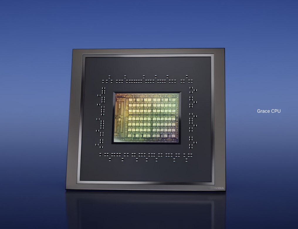
NVIDIA Moves to SOCAMM2, Phases Out Initial SOCAMM Design

NVIDIA has reportedly discontinued its first-generation Small Outline Compression Attached Memory Modules, known as SOCAMM. According to ET News, NVIDIA is shifting focus to the second-generation SOCAMM2 standard, which is being revamped for higher memory speeds, resulting in significantly improved bandwidth and performance. The first-generation SOCAMM was developed independently by NVIDIA, outside of any official memory consortium like JEDEC. It featured a detachable module design, offering superior specifications compared to existing solutions, with 694 I/O ports (compared to LPCAMM's 644 and traditional DRAM's 260), direct LPDDR5X memory substrate integration, and a more compact form factor.

NVIDIA aims for SOCAMM2 to become a faster, more widely adopted standard, potentially with JEDEC's assistance to standardize the format. SOCAMM2 is expected to maintain the same 649 I/O ports exposed to the motherboard but will integrate faster LPDDR5X running at 9600 MT/s, compared to the first-generation SOCAMM's 8533 MT/s. The new SOCAMM2 might also use LPDDR6 and source it from multiple suppliers. NVIDIA currently ships SOCAMM in its "Blackwell Ultra" GB300 NVL72 system, providing 18 TB of LPDDR5X memory at 14.3 TB/s bandwidth. An upgrade to SOCAMM2 could increase that to 16 TB/s bandwidth as a simple drop-in replacement, stemming from 9600 MT/s LPDDR5X. Additionally, NVIDIA may be diversifying its supplier strategy. The first-gen SOCAMM was supplied by Micron, but now Samsung and SK Hynix might join, although no specific details or timeline are available.

AMD Medusa Halo APU Leak Reveals Up to 24 Cores and 48 RDNA 5 CUs

A fresh leak has shed light on AMD's next-gen Medusa Halo APU that is set to launch in 2027 as the company's top-of-the-line chip (dismissing previous rumors about AMD cancelling Medusa Halo APU). Moore's Law is Dead has shared information suggesting Medusa Halo will pack Zen 6 CPU chiplets made using TSMC's cutting-edge N2P process, with the I/O die will be made using the N3P process. The base Medusa Halo APUs have 12 Zen 6 cores alongside 2 power-efficient Zen 6 LP cores, while high-end versions might include an extra 12-core Zen 6 CCD. This means AMD will provide Medusa Halo APUs with 24 CPU cores (and possible even up to 26 cores).

For graphics, the Medusa Halo APUs will feature 48 compute units (CUs) based on RDNA 5 architecture alongside 20 MB of L2 cache. This represents a significant jump from the 40 CUs in today's Strix Halo APU and should deliver graphics power on par with an NVIDIA GeForce RTX 5070 Ti, a big step forward for built-in GPUs. Memory support is in line for a big boost, with Medusa Halo set to offer either a 384-bit LPDDR6 or 256-bit LPDDR5X memory controller. This will provide high bandwidth to match its upgraded GPU needs.

Cadence Introduces Industry-First LPDDR6/5X 14.4 Gbps Memory IP to Power Next-Generation AI Infrastructure

Cadence today announced the tapeout of the industry's first LPDDR6/5X memory IP system solution optimized to operate at 14.4 Gbps, up to 50% faster than the previous generation of LPDDR DRAM. The new Cadence LPDDR6/5X memory IP system solution is a key enabler for scaling up the AI infrastructure to accommodate the memory bandwidth and capacity demands of next-generation AI LLMs, agentic AI and other compute-heavy workloads for various verticals. Multiple engagements are currently underway with leading AI, high-performance computing (HPC) and data center customers.

The Cadence IP for the JEDEC LPDDR6/5X standard consists of an advanced PHY architecture and a high-performance controller designed to maximize power, performance and area (PPA) while supporting both LPDDR6 and LPDDR5X DRAM protocols for optimal flexibility. The solution supports native integration into traditional monolithic SoCs as well as multi-die system architectures by leveraging the Cadence chiplet framework, enabling heterogeneous chiplet integration. The chiplet framework, including the previous LPDDR generation, was successfully taped out in 2024.

JEDEC Releases New LPDDR6 Standard to Enhance Memory Performance

JEDEC Solid State Technology Association, the global leader in standards development for the microelectronics industry, today announced the publication of JESD209-6, the latest Low Power Double Data Rate 6 (LPDDR6) standard. JESD209-6 is designed to significantly boost memory speed and efficiency for a variety of uses including mobile devices and AI. The new JESD209-6 LPDDR6 standard represents a significant advancement in memory technology, offering enhanced performance, power efficiency, and security.

High Performance
To enable AI applications and other high-performance workloads, LPDDR6 employs a dual sub-channel architecture that allows for flexible operation while maintaining a small access granularity of 32 bytes. In addition, LPDDR6 key features offer:
  • 2 sub-channels per die, 12 data signal lines (DQs) per sub-channel to optimize channel performance capabilities
  • Each sub-channel includes 4 command/address (CA) signals, optimized to reduce ball count and improve data access speed
  • Static efficiency mode designed to support high-capacity memory configurations and maximize bank resource utilization
  • Flexible data access, on-the-fly burst length control to support 32B & 64B access
  • Dynamic write NT-ODT (non-target on-die termination) enables the memory to adjust ODT based on workload demands, improving signal integrity

Synopsys Accelerates AI and Multi-Die Design Innovation on Advanced Samsung Foundry Processes

Synopsys, Inc. announced today its ongoing close collaboration with Samsung Foundry to power the next generation of designs for advanced edge AI, HPC, and AI applications. The collaboration between the companies is helping mutual customers achieve successful tape-outs of their complex designs using Synopsys' 3DIC Compiler and Samsung's advanced packaging technologies with fast turnaround time. Mutual customers can improve power, performance and area (PPA) with certified EDA flows for SF2P process, and minimize IP integration risk with the high-quality portfolio of IP on Samsung's most advanced process technologies.

"The adoption of Edge AI applications is driving the need for advancements in semiconductor technologies to enable complex computational tasks, improve efficiency, and expand AI capabilities across various industries and applications," said John Koeter, senior vice president for the Synopsys IP Group. "Together with Samsung Foundry, we're enabling the most advanced AI processors across a broad spectrum of use cases from high-performance AI inference engines for data centers to ultra-efficient Edge AI devices like cameras and drones, all optimized for development on sub-2 nm Samsung Foundry process technologies."

"Snapdragon 8 Elite Gen 2" SoC Tipped to Support LPDDR5X/LPDDR6 Memory

Late last month, speculative Snapdragon 8 Elite Gen 2 (aka SM8850) technical details emerged online. Up until then, Digital Chat Station's Weibo channel has delivered all sorts of pre-release information—mostly concentrating on Qualcomm's alleged redeployment of a familiar "2 + 6" core configuration, and selection of TSMC's 3 nm "N3P" node process. Earlier today, the veteran leaker predicted a couple of new-gen improvements—first concentrating on the alleged mobile chipset's "Adreno 840" integrated graphics solution. Digital Chat Station (DCS) believes that the company's engineering team has increased their iGPU design's independent cache size "from 12 MB to 16 MB," leading to: "early setting performance increased by 30%±." It is not clear whether this rumored upgrade has affected the SoC's L2 or L3 cache provisions, but the current-gen Snapdragon 8 Elite mobile processor makes do with 12 MB of L2 cache per cluster. Additionally, DCS reckons that an enlargement of caches has resulted in performance of Qualcomm's "second-generation self-developed CPU architecture" increasing "by 25%±."

As interpreted by Wccftech: "the upcoming SoC will now feature 32 MB of L2 cache, with the L3 count currently unknown at this time. The initial test results revealed that the 'Snapdragon 8 Elite Gen 2' delivered a 30 percent performance increase, but it is unconfirmed if this delta exists between the Snapdragon 8 Elite or some other silicon." DCS has heard whispers about the upcoming chip supporting "new generations of high-speed LPDDR5X/LPDDR6" memory. The mentioning of LPDDR5X is not surprising; given that the current Snapdragon 8 Elite model is already up to snuff with this spec. Just over a year ago, JEDEC was reportedly working on the finalization of LPDDR6 standards for mobile platforms. Shortly thereafter, smartphone industry watchdogs started to theorize about the arrival of a so-called "Snapdragon 8 Gen 4" chip with LPDDR6 RAM in 2025. Fast-forward to the present day; fresh reports suggest that manufacturers will have the option to outfit next-gen flagship devices with "bog-standard" LPDDR5X or faster/more efficient LPDDR6 memory.

Rivals Samsung and SK hynix Join Forces to Standardize LPDDR6-PIM Technology

Samsung Electronics and SK hynix are working together to standardize "Low Power Double Data Rate 6 (LPDDR6) - Processing in Memory (PIM)" technology according to a report from Business Korea. This collaboration seeks to accelerate the development of low power memory products. The cooperation is still in its early stage, the companies initial work is focused on registering the standard with the Joint Electron and Device Engineering Council (JEDEC). Discussions are underway to determine technical requirements, specific characteristics of LPDDR with PIM, such as "internal bandwidth"—the data transfer rate within the memory, unlike the "external bandwidth" between the processor and memory in traditional systems. According to a Samsung Electronics representative, the two companies are in the process of developing a timeline for standardization.

This partnership is notable given how Samsung and SK hynix compete in the high-bandwidth memory (HBM) market. SK hynix beat Samsung in profits reporting 7.3 trillion won in the third quarter, while Samsung made 3.86 trillion won. However, the rise of AI with its increased demand for more memory has shaken up the scene pushing for teamwork instead of wasting resources in developing completely different and unstandardized products. Both firms see PIM technology as a way to grow, previous attempts to independently develop PIM products include Samsung's HBM and LPDDR5-PIM and SK hynix's GDDR6-PIM.

JEDEC Unveils Plans for DDR5 MRDIMM and LPDDR6 CAMM Standards to Propel High-Performance Computing and AI

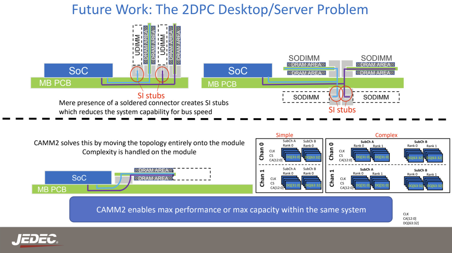
JEDEC Solid State Technology Association, the global leader in the development of standards for the microelectronics industry, proudly announces upcoming standards for advanced memory modules designed to power the next generation of high-performance computing and AI applications. JEDEC today revealed key details about its upcoming standards for DDR5 Multiplexed Rank Dual Inline Memory Modules (MRDIMM) and a next-generation Compression-Attached Memory Module (CAMM) for LPDDR6. The new MRDIMM and CAMM for LPDDR6 are set to revolutionize the industry with unparalleled bandwidth and memory capacity.

The JEDEC MRDIMM standard is set to deliver up to twice the peak bandwidth of native DRAM, enabling applications to surpass current data rates and achieve new levels of performance. It maintains the same capacity, reliability, availability, serviceability (RAS) features as JEDEC RDIMM. The committee aims to double the bandwidth to 12.8 Gbps and increase the pin speed. MRDIMM is envisioned to support more than two ranks and is being designed to utilize standard DDR5 DIMM components ensuring compatibility with conventional RDIMM systems.

NVIDIA's Arm-based AI PC Processor Could Leverage Arm Cortex X5 CPU Cores and Blackwell Graphics

Last week, we got confirmation from the highest levels of Dell and NVIDIA that the latter is making a client PC processor for the Windows on Arm (WoA) AI PC ecosystem that only has one player in it currently, Qualcomm. Michael Dell hinted that this NVIDIA AI PC processor would be ready in 2025. Since then, speculation has been rife about the various IP blocks NVIDIA could use in the development of this chip, the two key areas of debate have been the CPU cores and the process node.

Given that NVIDIA is gunning toward a 2025 launch of its AI PC processor, the company could implement reference Arm IP CPU cores, such as the Arm Cortex X5 "Blackhawk," and not venture out toward developing its own CPU cores on the Arm machine architecture, unlike Apple. Depending on how the market recieves its chips, NVIDIA could eventually develop its own cores. Next up, the company could use the most advanced 3 nm-class foundry node available in 2025 for its chip, such as the TSMC N3P. Given that even Apple and Qualcomm will build their contemporary notebook chips on this node, it would be a logical choice of node for NVIDIA. Then there's graphics and AI acceleration hardware.

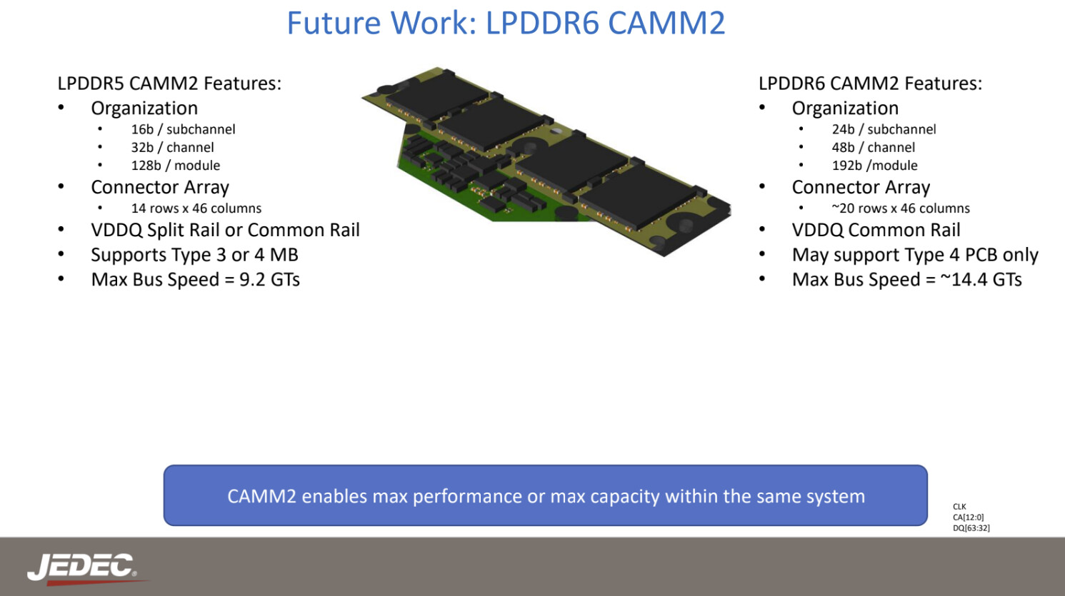
LPDDR6 LPCAMM2 Pictured and Detailed Courtesy of JEDEC

Yesterday we reported on DDR6 memory hitting new heights of performance and it looks like LPDDR6 will follow suit, at least based on details in a JEDEC presentation. LPDDR6 will just like LPDDR5 be available as solder down memory, but it will also be available in a new LPCAMM2 module. The bus speed of LPDDR5 on LPCAMM2 modules is expected to peak at 9.2 GT/s based on JEDEC specifications, but LPDDR6 will extend this to 14.4 GT/s or roughly a 50 percent increase. However, today the fastest and only LPCAMM2 modules on the retail market which are using LPDDR5X, comes in at 7.5 GT/s, which suggests that launch speeds of LPDDR6 will end up being quite far from the peak speeds.

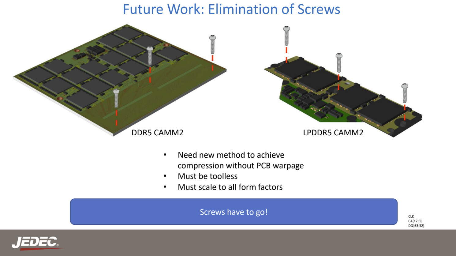
There will be some other interesting changes to LPDDR6 CAMM2 modules as there will be a move from 128-bit per module to 192-bit per module and each channel will go from 32-bits to 48-bits. Part of the reason for this is that LPDDR6 is moving to a 24-bit channel width, consisting of two 12-bit sub channels, as mentioned in yesterday's news post. This might seem odd at first, but in reality is fairly simple, LPDDR6 will have native ECC (Error Correction Code) or EDC (Error Detection Code) support, but it's currently not entirely clear how this will be implemented on a system level. JEDEC is also looking at developing a screwless solution for the CAMM2 and LPCAMM2 memory modules, but at the moment there's no clear solution in sight. We might also get to see LPDDR6 via LPCAMM2 modules on the desktop, although the presentation only mentions CAMM2 for the desktop, something we've already seen that MSI is working on.

PC DDR6 Memory to Offer 10-times the Bandwidth of DDR4: Synopsys

The next-generation PC DDR6 memory standard (not to be confused with GDDR6), will offer a 10-times increase in bandwidth over DDR4, according to a presentation by Synopsys, a major vendor of memory controller and PHY IP blocks. The initial draft of DDR6 specification by JEDEC is expected to be ready within 2024, with version 1.0 of the spec ready by mid-2025. Speeds (data-rates) of DDR6 start at DDR6-8800, and range up to DDR6-17600 in the first generation; with future generations of DDR6 going all the way up to DDR6-21333 (or 21 Gbps). This is exactly 10 times the bandwidth of DDR4-2133, the initial speed of DDR4 that debuted with 6th Gen Core "Skylake" processors, almost a decade ago. It hence makes sense for a memory specification 10 years since to offer such a linear scaling in bandwidth.

Synopsys also talks about LPDDR6 in this presentation, the future low power memory standard for thin-and-light computing devices and smartphones. LPDDR6 will have an introductory data-rate of LPDDR6-10667 over a 24-bit memory channel, with two 12-bit sub-channels. The highest defined data-rate for LPDDR6 is expected to be LPDDR6-14400 (likely 14466 MT/s). Besides generational increases in bandwidth, both PC DDR6 and LPDDR6 are expected to introduce several security and energy-efficiency features, including an "efficiency mode" that reduces idle power draw for the memory devices.
Return to Keyword Browsing
Nov 19th, 2026 01:07 PST change timezone

New Forum Posts

Popular Reviews

TPU on YouTube

Controversial News Posts