Friday, November 7th 2025

Samsung Prepares 10.7 Gbps LPDDR6 Memory Built on 12 nm Node
Samsung has developed its next-generation low-power LPDDR6 memory for mobile applications. Built on a 12 nm process, this LPDDR6 memory module achieves data rates of 10.7 Gbps. Engineers have increased the input/output channel count and introduced dynamic power tuning, which adjusts power consumption in real time based on workload demands. Samsung has also incorporated robust security features directly into the memory subsystem to ensure data integrity across all applications. Interestingly, Samsung's improved and tuned LPDDR5X also reaches 10.7 Gbps, which is the starting point for the new LPDDR6 memory.
As seen in the transition from DDR4 to DDR5, the final configurations of the previous generation memory are often close in performance to the first generation of the new standard. For LPDDR6, Samsung claims a 21% improvement in energy efficiency over its predecessor, LPDDR5X. This means devices can achieve the same bandwidth and speed while using one-fifth less power. Future LPDDR6 iterations are expected to reach speeds of up to 14 Gbps, surpassing even the fastest overclocked LPDDR5X chips. More details are anticipated at this year's CES, where Samsung will showcase devices powered by the new memory and reveal specific features.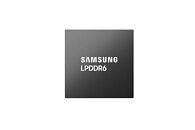
Sources:
CES, @harukaze5719
As seen in the transition from DDR4 to DDR5, the final configurations of the previous generation memory are often close in performance to the first generation of the new standard. For LPDDR6, Samsung claims a 21% improvement in energy efficiency over its predecessor, LPDDR5X. This means devices can achieve the same bandwidth and speed while using one-fifth less power. Future LPDDR6 iterations are expected to reach speeds of up to 14 Gbps, surpassing even the fastest overclocked LPDDR5X chips. More details are anticipated at this year's CES, where Samsung will showcase devices powered by the new memory and reveal specific features.

14 Comments on Samsung Prepares 10.7 Gbps LPDDR6 Memory Built on 12 nm Node
Just do a tush push on the ram chips & be happy !..
www.realworldtech.com/intel-dram/2/
17.5Mb/mm2 on 22nm.
semiwiki.com/forum/threads/techinsights-samsung-20-nm-ddr4-tsv-enabled-dram.5783/
1GB(8Gb) on 56mm2 die versus 128MB on 80mm2 die. It's 10x the density. This means a N3 logic node is needed to be at equal level density to 10nm DRAM node.
Both SRAM and DRAM are now made with EUV and both hardly scale anymore. To me it means that DRAM cell shrinking is limited both by minimum capacitor size and fab resolution.
Still, 4F²-sized DRAM cells are being researched, which would shrink the cell size by a third compared to today's 6F². Researchers know that the capacitor's area would have to be reduced by the same amount, so they probably have some ideas how to do that.
The 2nd physical limit is the wavelength of light which is several times larger than the size of the structures that this light is used to construct through lithography. We now have EUV and perhaps soft X-Ray machines in the future that shrink the wavelength of light but at some point, this will not shrink any further and we will be stuck permanently. There are workarounds for now like double-patterning and quad-patterning that delay the problem but it is still there and the workarounds add cost and time (which adds to the cost again).
A earlier form of scaling, Dennard scaling where the power usage of the transistor falls as the transistor size shrinks, already died in 2003. That started to increase costs as chip designers had to come up with power gating, dark silicon, etc to deal with a constrained power budget (which adds both development and product costs again).
This all feeds to the economical limit which is the cost of developing a new node, or a new product on that node. Both fab development costs and product development costs are increasing over time (related to the physical limit). This used to be compensated by shrinking the chip area, allowing for more products per wafer. Costs were spread out without cutting production because there were always more people to sell chips to.
There are two further limits on that, one market-related and one chip-design-related. There are not enough people to continue growing product volume so now the profit calculation around new nodes is more complicated. At each new node, customers have been delaying or just straight abandoning the transition to a new node because the economics don't make sense anymore. Only the largest companies have the product sales volumes to justify new nodes (Apple, etc).
The chip-design reason is that most cores spend their time waiting for data to arrive/leave instead of processing that data. Chip designs therefore must add different stages of memory/storage to reduce the time for data travel like cache, RAM, etc. The lowest latency solution is to put the memory directly on the die, right next to the logic transistors waiting for that data. But as others have explained, capacitance relies on internal volume so this shrinks slower than the logic transistors. Over time, more and more of the die area is cache which sabotages the economic scaling for a new node (adding costs again).
TLDR = Making smaller and smaller structures is damn hard and getting harder. All of this difficulty requires money to overcome.
This is all off the top amateur interest knowledge from a non-professional so take it with a grain of salt, I am sure I got half of the details wrong.
EDIT #1 = I feel like I used "limit" incorrectly here, most of these are not hard limits but obstacles to overcome that keep increasing in difficulty.
EDIT #2 = Wire resistance is another physical limit, wire scaling is vastly slower than transistor logic (thank you, Wirko)
Anyways, has anyone announced any processors with a LPDDR6 memory controller already?