News Posts matching #PCIe Gen 6

Return to Keyword Browsing

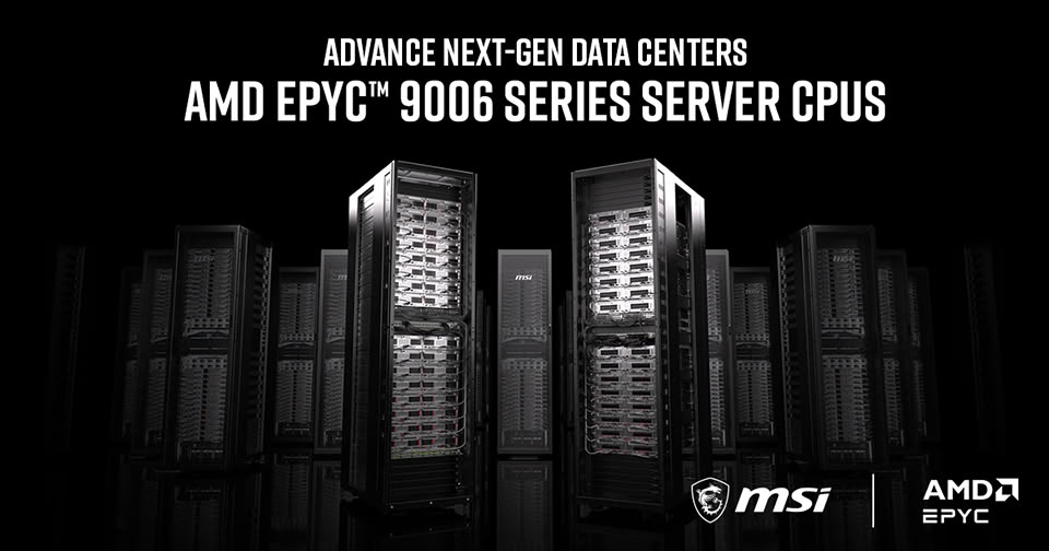
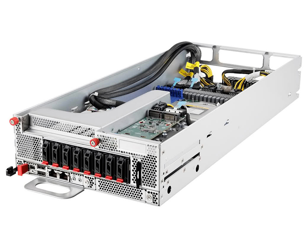
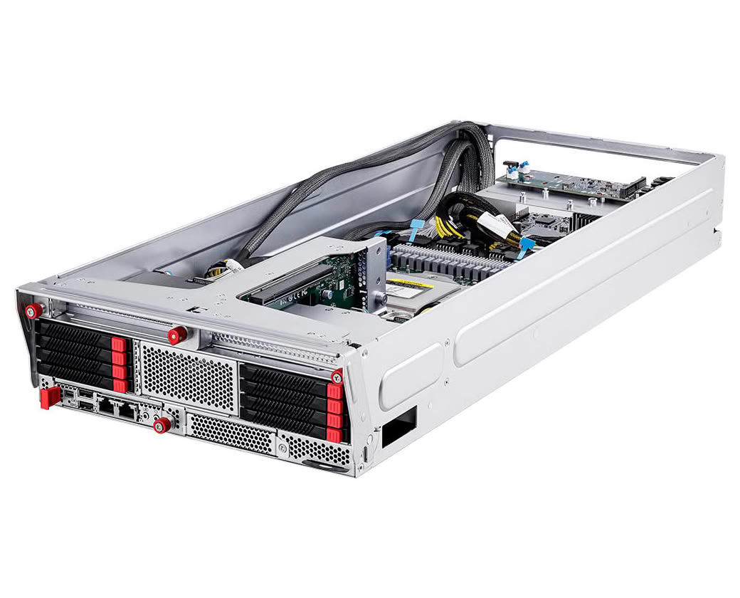
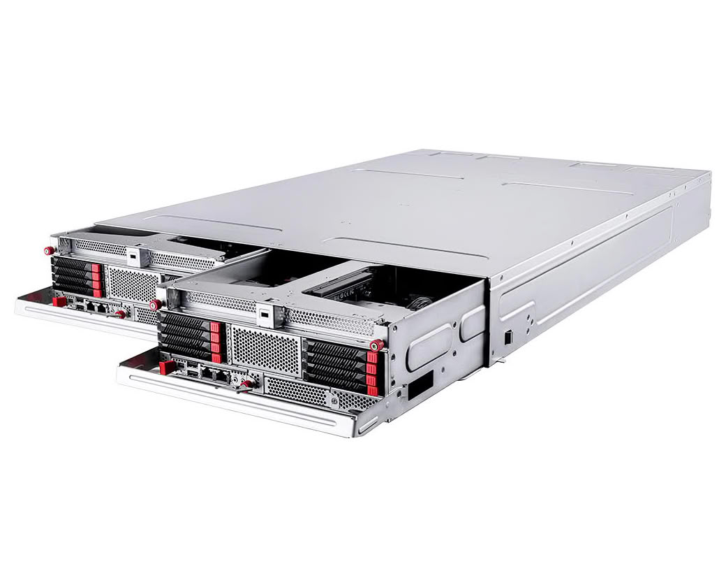
MSI Advances Next-Gen Data Center Infrastructure with AMD EPYC 9006 Series Server CPUs

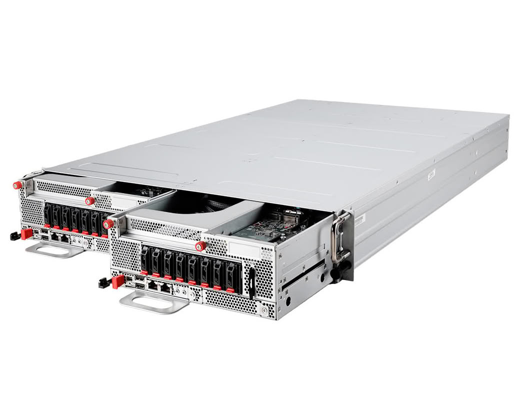
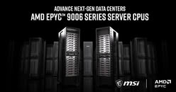
As agentic AI drives new demands for compute density, memory bandwidth, and data movement, MSI is advancing next-generation data center infrastructure with server platforms powered by AMD EPYC 9006 Series SP7 Server CPUs. With SP7 systems entering the shipping phase in Q4 2026 and SP8 platforms planned for the first half of 2027, MSI's portfolio spans liquid-cooled GPU servers, 19" DC-MHS and 21" ORv3 multi-node platforms, and enterprise servers, supporting AI, cloud, HPC, virtualization, and business-critical workloads.

Built on the Zen 6 architecture, AMD EPYC 9006 Series Server CPUs deliver up to 256 cores and 512 threads per socket for high-density computing and AI agent execution. With up to 1.6 TB/s of memory bandwidth and PCIe Gen 6 connectivity, they support data-intensive workloads and high-speed I/O for GPUs, networking, and storage.
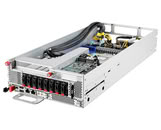
HPE Announces ProLiant Gen13 Servers Powered by 6th Gen AMD EPYC CPUs

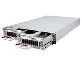
HPE (NYSE: HPE) today announced the first four of its HPE ProLiant Gen13 Servers powered by 6th Generation AMD EPYC Server processors. The new systems expand compute, memory, and I/O capabilities to help enterprises accelerate agentic AI and inference, analytics, virtualization, simulation, and modeling while strengthening security, simplifying operations, and providing reliability across distributed IT environments.

As AI systems evolve from generating insights to taking autonomous action, trust becomes a prerequisite for scale. McKinsey's 2026 AI Trust Maturity Survey found that nearly two-thirds of respondents cited security and risk concerns as the top barrier to fully scaling agentic AI. Within this evolving landscape, HPE ProLiant Gen13 helps customers address security and operational barriers with a trusted infrastructure foundation that combines HPE iLO 8 innovations for automatic protection, infrastructure trust, and post-quantum readiness with enhanced visibility and control from HPE Compute Ops Management.

Apple Introduces New Mac Studio with M5 Max and M5 Ultra

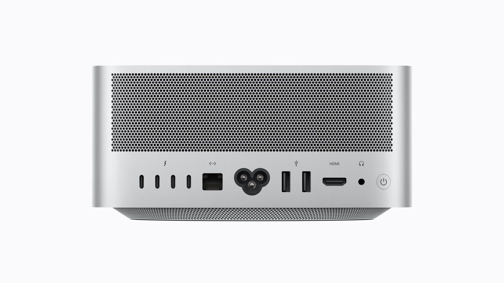
Apple today announced the new Mac Studio, featuring M5 Max and the all-new M5 Ultra, delivering a monumental leap in AI performance and even faster graphics for the most demanding pro workflows, all in its signature compact design that lives right on a user's desk. Now featuring up to 4.3x faster AI performance, up to 2x faster storage, up to 1.8x faster graphics, and up to 1.3x faster CPU speed, along with higher memory bandwidth, Mac Studio empowers creatives, developers, AI researchers, data scientists, and more to push the boundaries of what they can do. Mac Studio with M5 Max features an 18-core CPU, an up-to-40-core GPU with Neural Accelerators built into each core, and up to 128 GB of unified memory, accelerating complex pro and AI workloads.

With the powerful M5 Ultra, Mac Studio scales up to a 36-core CPU, up to an 80-core GPU, and a staggering 512 GB of unified memory, enabling users to run enormous LLMs entirely on device. Wi-Fi 7 and Bluetooth 6 come to Mac Studio for the first time, while Thunderbolt 5 rounds out its extensive connectivity, so users can take advantage of blazing-fast external storage, PCIe expansion chassis, and powerful hub solutions for the most intense workloads. Thunderbolt 5 also enables multiple Mac Studio systems to be clustered, bringing up to 3x faster performance for distributed AI inference when compared to a single system. Together with Studio Display and Studio Display XDR, along with the power of macOS 27 and the next generation of Apple Intelligence, including Siri AI, it is the ultimate pro desktop. The new Mac Studio is available for pre-order starting today, with availability beginning September 22.

Silicon Motion Showcases Next-Generation Storage Solutions for Agentic AI Applications at FMS 2026

Silicon Motion Technology Corporation ("Silicon Motion"), a global leader in designing and marketing NAND flash controllers for solid-state storage devices, today announced it will showcase its latest storage innovations for AI Factory, Edge AI, and Physical AI applications at Future of Memory and Storage (FMS) 2026, taking place August 4 to 6 in Santa Clara, California, at Booth #315.

As AI evolves beyond large language model training toward Agentic AI, real-time inference has become increasingly dependent on fast, predictable data access. Emerging storage requirements for KV cache and Agentic AI applications demand storage solutions that maximize acceleration while maintaining low latency and consistent performance. Silicon Motion will showcase five major product lines addressing the evolving storage requirements across the three AI segments, supporting enterprise infrastructure, edge computing, embedded devices, and automotive platforms:

Marvell Introduces Bravera SC6 SSD Controller for PCIe Gen 6 NVMe SSDs

As PCIe Gen 6 storage becomes increasingly important for AI infrastructure, cloud platforms, enterprise databases, and hyperscale data centers, SSD controllers must deliver significantly more than raw bandwidth. They need intelligent flash management, enterprise-grade security, advanced error correction and scalable architecture.

The Marvell Bravera SC6 SSD Controller (MV-SF1410) addresses these challenges by combining PCIe Gen 6 connectivity, NVMe 2.2 compliance, support for high-speed NAND flash, powerful multicore processing, integrated security and advanced reliability technologies into a single enterprise-ready platform. The Marvell Bravera SC6 SSD Controller (MV-SF1410) is engineered to meet the demanding requirements of modern data centers and enterprise storage environments. Designed to support PCIe Gen 6 NVMe SSDs, this advanced controller combines exceptional performance, scalability, robust security and intelligent flash management.

Microchip Partners with Micron to Showcase High-Performance PCIe Gen 6 Storage Architecture

Microchip Technology (Nasdaq: MCHP) today announced a demonstration showcasing an end-to-end PCIe Gen 6 storage architecture, combining Microchip's Switchtec PCIe Gen 6 switches with high-performance Micron 9650 NVMe solid state drives (SSDs). The demonstration highlights the role of next-generation PCIe technology in enabling higher data throughput, reduced latency and scalable connectivity for AI, high-performance computing (HPC) and cloud data center workloads.

At the 2026 Future of Memory and Storage (FMS) Conference, the demonstration features a Microchip Switchtec Gen 6 PCIe fanout switch acting as a high-bandwidth, low-latency interconnect between host processors and multiple Micron 9650 SSDs enabling the drives to operate at the full potential of Gen 6 speed. The architecture supports composable and disaggregated system designs, allowing data center architects to scale storage resources efficiently while maintaining predictable performance.

ScaleFlux Unveils PCIe Gen 6 SSD and CXL Memory Controllers

ScaleFlux will introduce two next-generation PCIe Gen 6 silicon solutions at Future of Memory and Storage (FMS) 2026: the FC6116 PCIe Gen 6 NVMe SSD Controller and the MC600 PCIe Gen 6 CXL 3.2 Type 3 Memory Controller. Together, these products expand ScaleFlux's portfolio of high-performance storage and memory controller technologies, enabling AI, hyperscale cloud, and enterprise infrastructure with higher bandwidth, lower power consumption, and greater scalability. Beyond silicon, ScaleFlux differentiates itself by delivering a complete turnkey solution, including production-ready firmware, validated reference designs, and contract manufacturing partner support, enabling customers to accelerate development, simplify qualification, and bring products to market faster.

"AI infrastructure is driving unprecedented demand for higher bandwidth, greater memory capacity, and lower power consumption," said Hao Zhong, CEO and Co-founder of ScaleFlux. "With the introduction of FC6116 and MC600, ScaleFlux is extending its silicon platform into the PCIe Gen 6 era, giving customers the building blocks to design faster, more efficient, and more flexible storage and memory systems."

AMD Advancing AI 2026: Pensando "Salina" DPU and "Vulcano" AI NIC Power Helios Networking

Networking is the third pillar of AMD's Advancing AI 2026 rack-scale strategy, and today the company detailed the AMD Pensando silicon and fabric technology that connects the Helios rack. As Helios is AMD's first rack-scale design, the company encountered challenges in interconnecting many GPUs, memories, and data movement speeds within a single system, both for scaling up and scaling out for multi-rack connections inside the data center. Current AI infrastructure must closely follow model development as AI model sizes have grown exponentially, from the original 65-million-parameter Transformer in 2017 to trillion-parameter GPT-4-class systems and now 10-trillion-plus parameter agentic and reasoning models. To run a model with more than 10 trillion parameters, you need to connect dozens of GPUs with high-speed VRAM, as well as a high-speed interconnect to split model weights effectively so latency isn't an issue. The modern interconnect of choice is again the plain-old Ethernet, not proprietary interconnects, which have become the standard for AI networking.

AMD's solution spans three layers: a third-generation Pensando "Salina" DPU on the front end, a first-generation UALink-over-Ethernet (UALoE) scale-up fabric inside the rack, and a second-generation Pensando "Vulcano" AI NIC for scale-out. All of this is managed by AMD's Helios management software and Fabric Manager. AMD outlined challenges that bandwidth needs are doubling in less than two years driven by massive AI models growing at a rapid pace, and that the hardware iteration cycles need to account for intelligence in the data fabric layer, not only compute layer.

ASRock Rack Unveils Next-Generation Server Portfolio Powered by 6th Gen AMD EPYC Processors

ASRock Rack Inc., a leading innovative server company, today announced support for the newly-launched 6th Gen AMD EPYC 9006 Series processors, unveiled this week at AMD Advancing AI 2026 in San Francisco. ASRock Rack will showcase its upcoming server platforms optimized for the new processor generation at the event, demonstrating its commitment to delivering advanced infrastructure for enterprise AI, cloud, and HPC workloads.

Delivering Leadership Performance for the Agentic AI Era
As agentic AI enters enterprise-scale deployment, the 6th Gen AMD EPYC 9006 Series processors deliver the performance, efficiency, and scalability required to support increasingly complex AI services and applications. Featuring up to 256 cores, industry-leading 5 GHz frequencies, and PCIe Gen 6 connectivity, 6th Gen EPYC Server CPUs enable organizations to scale AI agents, maximize AI host-node throughput and GPU utilization, and power the general-purpose workloads essential to modern data centers.

Giga Computing Accelerates Enterprise AI at Scale with 6th Gen AMD EPYC Server CPUs

Giga Computing, a subsidiary of GIGABYTE, is a global provider of advanced computing solutions that power the next generation of HPC, AI inference, 5G/edge, and cloud computing, today announced support for 6th Gen AMD EPYC Server CPUs across its server lineup, further expanding its portfolio of systems designed for demanding workloads. Now, at AMD Advancing AI 2026 in San Francisco, Giga Computing is debuting its first server for the new AMD EPYC 9006 platform.

Two Sockets, One Generation
With 6th Gen AMD EPYC Server CPUs, AMD introduces a two-socket strategy to serve the diverse workloads of the modern data center. The larger SP7 socket delivers leadership performance for the agentic AI era, with industry-leading memory bandwidth and PCIe Gen 6 connectivity, and the SP8 socket delivers efficient scale-out performance where density is the goal. Both sockets can be equipped with AMD performant "Zen6" or density "Zen6c" cores to fit the architecture of any deployment.

NVIDIA Details the "Rubin" Architecture: Die Annotation, Vera CPU, HBM4, and Disaggregated Inference

NVIDIA has released a technical details on its next-generation "Rubin" GPU, including a fully annotated die shot. "Rubin" represents a significant generational leap in NVIDIA's mission to scale computing across numerous racks, systems, and data centers. The company is promoting this generation as the first "agentic AI" native design. This AI paradigm means that inference workloads are continuously active, engage in reasoning, planning, tool utilization, and execute many sequential steps. In this context, inference refers to a completed model running on the GPUs, rather than being trained, which is what Rubin is designed for. NVIDIA claims up to 10x more agentic throughput per unit of energy compared to "Blackwell." This improvement relies not only on the new "Vera" CPU and rack-level power management but also on the entire system, as customers now prioritize overall system performance rather than just the performance of a single GPU.

In its full configuration, "Rubin" combines two compute dies in a single package, linked with a high-speed connection that NVIDIA calls NV-HBI. This chiplet approach uses CoWoS-L packaging from TSMC, chosen because each die is already as large as the chip factory can print in one go, reaching the reticle limit. The GPU contains 336 billion transistors, up to 224 SMs, 896 Tensor Cores with a third-generation Transformer Engine, and 288 GB of HBM4 memory, capable of delivering up to 50 PetaFLOPS of inference and about 35 PetaFLOPS of training at the ultra-compact NVFP4 format. This is NVIDIA's proprietary 4-bit data format that enhances efficiency in inference and training with minimal to no accuracy loss compared to the 8-bit and 16-bit data formats used today for training and inference. However, this is quite different from the FP16/FP32 formats used in gaming GPUs. Below, we will break down not just the GPU, but the entire platform NVIDIA has built around it.

Longsys Achieves One Million Monthly mSSD Production Capacity, Accelerating Edge AI Storage Deployment

Longsys announced the establishment of a stable monthly production and delivery capacity of one million mSSD (Micro SSD) units, marking a major milestone for its high speed mSSD storage solutions. The new production capacity is designed to meet growing market demand while providing room for future expansion.

The first mSSD samples rolled off the production line at Longsys' Suzhou packaging and testing manufacturing base in October 2025. Following production line optimization, process refinement and manufacturing ramp-up, Longsys established a stable monthly production capacity of one million units in June 2026. Leveraging SiP (System-in-Package) integration and packaging technology to innovate and evolve traditional storage form factors, the product's performance, quality and functionality have been validated through real-world customer applications, and the company is now working with leading industry customers, including Lenovo and ASUS.

AWS Graviton5 Enterprise Processor Pictured

Here are some of the first pictures of the AWS Graviton5, the company's in-house server processor designed by Annapurna Labs, which it developed not just for running its own server infrastructure, but also its AI inferencing infrastructure. The package has four chiplets, each built on the TSMC 3 nm foundry node. It has a total CPU core count of 192, all of which are Arm V3 performance cores with 1 MB of dedicated cache. The package has a 12-channel DDR5 memory interface that supports speeds of up to DDR5-8800 for whole-package memory bandwidth of over 800 GB/s. It also features a 96-lane PCI-Express Gen 6 root complex.

Although a disaggregated chip, AWS designed the Graviton 5 to feature full cache coherency among its chiplets, enabled by its 420 GB/s die-to-die interconnect bandwidth. Each chiplet has a quarter of the package's resources—48 Arm V3 cores, 3-channel DDR5 IMC, and a 24-lane PCIe Gen 6 root complex. AWS is gunning for a 25% performance improvement over the company's AWS G4 instances that are powered by Intel Xeon Scalable "Cascade Lake" or AMD EPYC "Genoa" processors.

Phison and Pascari at Computex 2026: New PCIe Gen 6 X3 and E37T DRAMless Gen 5 Controllers, Lots More

Phison at the 2026 Computex showcased its next-generation SSD controllers based on new foundry nodes, implementing new PCI-Express Gen 6 (256 Gbps), and its reference SSD demos. The company also unveiled its newest Pascari-branded enterprise SSDs. We begin our tour with the new Phison X3 series 8-channel SSD controller that implements PCIe Gen 6, the future interconnect standard that could debut in 2027-28. The controller features a PCI-Express 6.0 x4 host interface, and supports NVMe 2.3 protocol, including computational storage. While there are no host platforms besides development kits handed out by Intel, a Gen 6 SSD powered by the X3 will typically offer sequential transfer rates of 28 GB/s, double that of today's Gen 5 SSDs, with 4K random access speeds of up to 6.8 million IOPS.

Next up is the new Phison E37T, the successor to the E27T. This is a very interesting PCIe Gen 5 client SSD controller that's DRAMless, while offering sequential speeds of up to 14.9 GB/s reads, with up to 13.2 GB/s writes—performance you'd expect from a high-end controller with DRAM cache. It also tops out at 3 million IOPS 4K random access. The best part? Phison claims an active power of under 2.3 W, which means drives based on this chip can make do without any active cooling, perhaps just a heat-spreader or a lightweight heatsink. Phison showed us their reference SSD based on the E37T, along with a performance demo.

Arm Enters Silicon Business for the First Time with Data Center AGI CPU

Arm has made a significant move stepping into production silicon for the first time in its history with the launch of the Arm AGI CPU, a data center processor designed specifically for agentic AI workloads. For over three decades, Arm has been purely an IP licensing business. With the launch of its AGI CPU series, Arm made a fundamental shift in how the company positions itself in the market. The AGI CPU is built on a 3 nm process, packs up to 136 Neoverse V3 cores, runs at a 300 W TDP, and delivers 6 GB/s of memory bandwidth per core at under 100 ns latency. It supports up to 6 TB per chip and DDR5-8800 speeds. On the I/O side, the chip features 96 PCIe Gen 6 lanes along with CXL 3.0 and AMBA CHI (Coherent Hub Interface) links. Each core handles a dedicated program thread, which Arm says eliminates throttling and idle threads under sustained load.

Specifically important in the data center business, density figures are notable. Air-cooled systems can fit up to 8,160 cores per rack, while liquid-cooled systems push that above 45,000. Data centers are expected to need more than four times the current CPU capacity per gigawatt to keep up, and Arm is arguing that x86 architecture carries too much overhead and complexity for this new class of workload. Arm claims more than 2x performance per rack versus x86, adding that this can translate to potential savings of up to $10 billion per gigawatt of AI data center capacity.

MSI Launches XpertStation WS300 on NVIDIA DGX Station Architecture

MSI today announced the launch of XpertStation WS300 on NVIDIA DGX Station Architecture, a next-generation deskside AI supercomputer built to support the accelerating demands of large language models (LLMs), generative AI, and advanced data science workflows. Powered by NVIDIA GB300 Grace Blackwell Ultra Desktop Superchip, supporting up to 748 GB of large coherent memory and dual 400GbE networking, the platform extends advanced AI infrastructure capabilities into a compact deskside deployment model and is available for order starting today.

"MSI has a strategic vision to advance AI-first computing," said Danny Hsu, General Manager of MSI's Enterprise Platform Solutions. "With NVIDIA, we are defining the next era of AI infrastructure, bridging centralized performance and distributed innovation, and enabling organizations to move from experimentation to production with greater speed, scale, and confidence."

Micron 9650 PCIe Gen 6 SSDs Enters Mass Production

Micron announced its 9650 NVMe SSD has entered mass production, making it the first PCIe Gen 6 data center drive to reach this milestone. The series was first unveiled in July 2025, and it features Micron G9 TLC NAND, including Micron designed SSD controller ASIC, DRAM, and Micron produced and validated firmware. The Micron 9650 delivers up to 28 GB/s in sequential reads, double that of PCIe Gen 5 drives. The drive's sequential write speed reaches 14 GB/s, while its random read performance hits 5.5 million IOPS and its random write achieves 900,000 IOPS. These numbers show 100%, 40%, 67%, and 22% gains over Gen 5. At a 25-watt power state, the drive offers double the performance of PCIe Gen 5 options. It has a sequential read efficiency of 1,120 MB/s per watt (2× better than Gen 5), and its sequential write efficiency is 560 MB/s per watt (1.4 times better). The random read efficiency stands at 220 KIOPS per watt (1.7 times higher) and random write at 36 KIOPS per watt (1.2 times improved).

The Micron 9650 supports both air-cooled and liquid-cooled configurations to handle higher performance densities in modern data centers. Micron conducted 18 months of interoperability testing across the PCIe Gen 6 ecosystem, including validation with high-port switches, retimers, and demonstrations at industry events. The drive is now being qualified by OEM and AI data center customers for deployment in AI training and inference workloads, particularly those requiring high-throughput data access for large language models and retrieval-augmented generation pipelines. The Micron 9650 is available in E1.S and E3.S form factors with E1.S available for liquid cooling.

SK hynix Targets 100M IOPS NAND by 2027 in Joint Effort with NVIDIA

SK hynix is pushing hard on next-gen AI NAND, and 2027 seems to be its next major milestone. According to a ZDNet report, the company is working with NVIDIA to build ultra-fast AI-focused NAND chips that could hit up to 30x the performance of today's enterprise SSDs. Early samples are planned for late 2026, with second-gen entering mass production by the end of 2027. A big part of that effort is SK hynix AI-N P high-performance SSD architecture aimed at removing I/O bottlenecks in large AI inference workloads. ZDNet says the redesigned NAND and controller are already in proof-of-concept (PoC) testing with NVIDIA. SK hynix is targeting 25 million IOPS on PCIe Gen 6 for first samples next year, and 100 million IOPS for the production version in 2027. For comparison, current enterprise SSDs manage roughly 2-3 million IOPS (high-end models).

The roadmap also includes AI-N B, better known as HBF (High Bandwidth Flash), developed with Sandisk. An alpha spec is expected in early 2026 with evaluation units coming in 2027. Behind all these efforts a broader strategy starts to unveil with SK hynix next-gen AI-NAND chips split into three. First we have AI-N P (ultra-high performance SSD) for performance, AI-N B (High Bandwidth Flash) for bandwidth, and AI-N D (High Capacity/Low Cost SSD) for higher-capacity and lower-cost designs. ZDNet adds that SK hynix views the AI market as two distinct fronts: large data-center deployments demanding massive throughput, and on-device AI favoring low-power efficiency. SK hynix is positioning its AI-N lineup to serve both with the 2026 AI-N P generation expected to offer roughly 8-10x the performance of current SSDs.

Panmnesia Samples Industry's First PCIe 6.0/CXL 3.2 Fabric Switch

Panmnesia, a pioneer in AI infrastructure link solutions, announced sample availability of its PCIe 6.0/CXL 3.2 Fabric Switch—the industry's first CXL switch silicon supporting port-based routing (PBR). The company is currently in the process of providing switch silicon samples to early access partners.

Panmnesia's switch is a hybrid solution that supports both PCIe Gen 6 and CXL 3.2 protocols on a single chip, while maintaining full backward compatibility with all previous PCIe and CXL generations. Fully implemented in strict accordance with the CXL 3.2/PCIe 6.0 specifications, it ensures complete standards compliance and seamless interoperability across all subprotocols. The switch can also operate in PBR mode and hierarchy-based routing (HBR) mode.

Microchip Unveils First 3 nm PCIe Gen 6 Switch

As artificial intelligence (AI) workloads and high-performance computing (HPC) applications continue to drive unprecedented demand for faster data movement and lower latency, Microchip Technology (Nasdaq: MCHP) has introduced its next generation of Switchtec Gen 6 PCIe Switches. The industry's first PCIe Gen 6 switches manufactured using a 3 nm process, the Switchtec Gen 6 family is designed to deliver lower power consumption and support up to 160 lanes for high-density AI system connectivity. Advanced security features include a hardware root of trust and secure boot, utilizing post-quantum safe cryptography compliant with the Commercial National Security Algorithm Suite (CNSA) 2.0.

Previous PCIe generations created bandwidth bottlenecks as data transferred between CPUs, GPUs, memory and storage, leading to underutilization and wasted compute cycles. PCIe 6.0 doubles the bandwidth of PCIe 5.0 to 64 GT/s (giga transfers per second) per lane, providing the necessary data pipeline to keep the most powerful AI accelerators consistently supplied. Switchtec Gen 6 PCIe switches enable high-speed connectivity between CPUs, GPUs, SoCs, AI accelerators and storage devices, and are designed to help data center architects scale to the potential of next generation AI and cloud infrastructure.

Samsung Targets 256 TB PCIe 6.0 SSD in 2026, 512 TB Capacity in 2027

At the 2025 Global Memory Innovation Forum in Shenzhen, China, Samsung confirmed it will ship its next-generation CXL 3.1 and PCIe 6.0 CMM-D storage products. Kevin Yoo, Samsung's Memory BU CTO, outlined a practical timeline for the company's upcoming storage solutions. The PM1763 Gen 6 SSD is expected to launch in early 2026, offering about twice the performance of its predecessor while maintaining power consumption around 25 watts. Following the release of 256 TB Gen 5 drives in 2026, Samsung plans to introduce a 512 TB PCIe Gen 6 unit around 2027 in the 1T EDSFF format. Additionally, a seventh-generation Z-NAND with GIDS, referred to as memory-class storage, is scheduled for 2026.

Samsung had previously showcased its PM1763 256 TB SSD at the Future of Memory Storage 2025 event in August. The company first demonstrated a working prototype of the 256 TB unit, initially hinted at in 2023. However, at the FSM event, it was revealed that the SSD is nearing readiness for market release. With a completely redesigned capacitor, controller, and DRAM layout, it appears Samsung is focusing on optimizing cooling and performance efficiency for these high-capacity drives. High-capacity SSDs are of significant interest to AI labs, especially as data requirements for training continue to grow. The exact timelines and release dates of these SSDs is unknown, and Samsung may change specific date as it irons out any remaining power/thermal issues it encounters in these high-capacity drives.

AMD "Zen 6" Processors to Use TSMC 2 nm Node for CCDs, 3 nm for IOD

AMD will transition its next-generation "Zen 6" desktop Ryzen and server EPYC processors to a split-node strategy, placing CPU core complex die (CCD) on TSMC N2P 2 nm node variant and building the I/O die (IOD) on the N3P 3 nm node. At TSMC, volume ramp for the 2 nm node is around the third quarter of 2026, opening the door for limited shipments as early as late Q3 or broader availability in Q4 2026. Under the split approach, the compute chiplet will house the Zen 6 cores and a substantially larger shared L3 pool, while the IOD will continue to host memory controllers, PCIe lanes, USB, and the integrated GPU. Earlier rumors suggest that each CCD could contain 12 Zen 6 cores with support for SMT, and a shared L3 cache that may increase to roughly 48 MB per CCD compared with prior generations. Typical consumer configurations would pair up to two CCDs with a single IOD, creating chips with up to 24 cores and 48 threads, while server variants could scale further depending on packaging.

Performance expectations center on achieving double-digit IPC gains, higher sustained clock speeds, and improved power efficiency, thanks to the advanced process nodes. The choice of N3P for IOD helps AMD cut some costs for non-core logic, while the N2P compute die aims to extract greater generational gains. However, as with any new TSMC node, it will carry a premium over the N3P, so using it only for the compute side is the most viable choice. Platform compatibility remains for one more generation, with Zen 6 expected to support the existing AM5 socket. Users can upgrade CPUs without a full platform replacement. If the ramp timing holds, Zen 6 will arrive into a crowded second half of 2026 desktop window. For datacenter applications, the EPYC "Venice" generation, based on Zen 6, will utilize sIOD (server I/O die), implementing PCIe Gen 6, which provides a generational doubling in bandwidth to GPUs, SSDs, and NICs. AMD is also claiming memory bandwidth of up to 1.6 TB/s for these CPUs, so we could see some of that trickling down into consumer configurations.

AMD Prepares EPYC "Venice" Platform to Break the 1,000 W Power Barrier

The kilowatt era of CPUs is upon us, as AMD is preparing specialized cooling for its next-generation SP7 socket powering EPYC "Venice". During the OCP APAC 2025 Summit in early August, Microloops held a presentation dedicated entirely to system-level cooling using custom high-performance cold plates, cooling distribution units, and much more. However, an interesting tidbit is the mention of AMD and its plan to likely cool CPUs with TDPs ranging from 700 to 1400 W. This marks AMD's first step into a kilowatt-level chip design, requiring kilowatt-level cooling. AMD is preparing to roll out its Zen 6 microarchitecture in 2026, with a server-focused flagship called EPYC "Venice." The new platform is expected to significantly increase core counts, utilizing full-sized Zen 6 cores and an updated I/O subsystem to target much stronger multithreaded throughput. AMD is reportedly configuring Venice to support as many as 256 CPU cores in a single package, a big leap intended to sharpen its position in dense compute environments.

Under the hood, Zen 6 CCDs are planned for TSMC's 2 nm N2 node, while the server I/O die will bring next-generation connectivity with PCIe Gen 6, doubling raw device bandwidth for GPUs, NVMe storage, and high-speed NICs. AMD has also pointed to memory bandwidth claims of up to roughly 1.6 TB/s, which could be achieved through faster DRAM clocks, expanding the memory controller to a 16-channel DDR5 layout from the current 12 channels, or supporting multichannel DIMM formats such as MR-DIMM and MCR-DIMM. Taken together, AMD says Venice will deliver approximately a 70% improvement in multithreaded performance compared to the current EPYC "Turin" family. However, all of that is shaping up to come with a significant power cost, as AMD gears up to cool these chips through customized solutions.

NVIDIA "Blackwell Ultra" Brings PCIe Gen 6 and 1.5x NVFP4 Performance Boost

NVIDIA's long-anticipated "Blackwell Ultra" is the final form of the Blackwell family before the transition to "Rubin." However, this silicon doesn't seem to share much resemblance with its predecessors, especially in terms of I/O and performance. On its blog, NVIDIA detailed the silicon design of its latest creation and all the accompanying features like enhanced software support and optimizations. One of the most striking aspects of the Blackwell Ultra, designed for AI servers, is its use of PCIe Gen 6, whereas the consumer Blackwell and regular server Blackwell use PCIe Gen 5. Made using the TSMC 4NP node, the massive Ultra chip features 208 billion transistors, which is 2.6 times more than the last generation Hopper, based solely on raw transistor count. This comes with a 1,400 W TDP, which means a massive cooling system is a must.

When it comes to performance, Blackwell Ultra delivers approximately 1.5 times denser NVFP4 compute compared to Blackwell, resulting in higher tokens-per-second on inference and improved throughput for large-batch training. The chip pairs 160 SMs across two reticle dies via NVIDIA's NV-HBI link, bringing a 10 TB/s die-to-die fabric, 288 GB of HBM3E at up to 8 TB/s bandwidth, and fifth-generation Tensor Cores tuned for NVFP4. Attention-layer throughput benefits from the doubled performance of special function units (SFUs) for transcendental operations, reducing softmax latency and enhancing reasoning responsiveness.
Blackwell Ultra Blackwell Ultra Blackwell Ultra

XConn Technologies to Demo End-to-End PCIe Gen 6 at FMS25

XConn Technologies (XConn), the innovation leader in next-generation interconnect technology for high-performance computing and AI workloads, today announced that it will deliver a live, end-to-end PCIe Gen 6.2 and CXL 3.1 technology demonstration at the Future of Memory and Storage (FMS25) event, taking place August 5-7 at the Santa Clara Convention Center in booth #1245.

The demonstration will highlight how XConn's advanced switching solutions can enable next-generation systems with ultra-high bandwidth, extremely low latency, and seamless support for emerging memory and accelerator architectures. Attendees will see first-hand how Peripheral Component Interconnect Express (PCIe) Gen 6.2 and Compute Express Link (CXL) 3.1 technologies are driving the future of composable infrastructure and disaggregated computing.
Return to Keyword Browsing
Nov 11th, 2026 03:59 CST change timezone

New Forum Posts

Popular Reviews

TPU on YouTube

Controversial News Posts