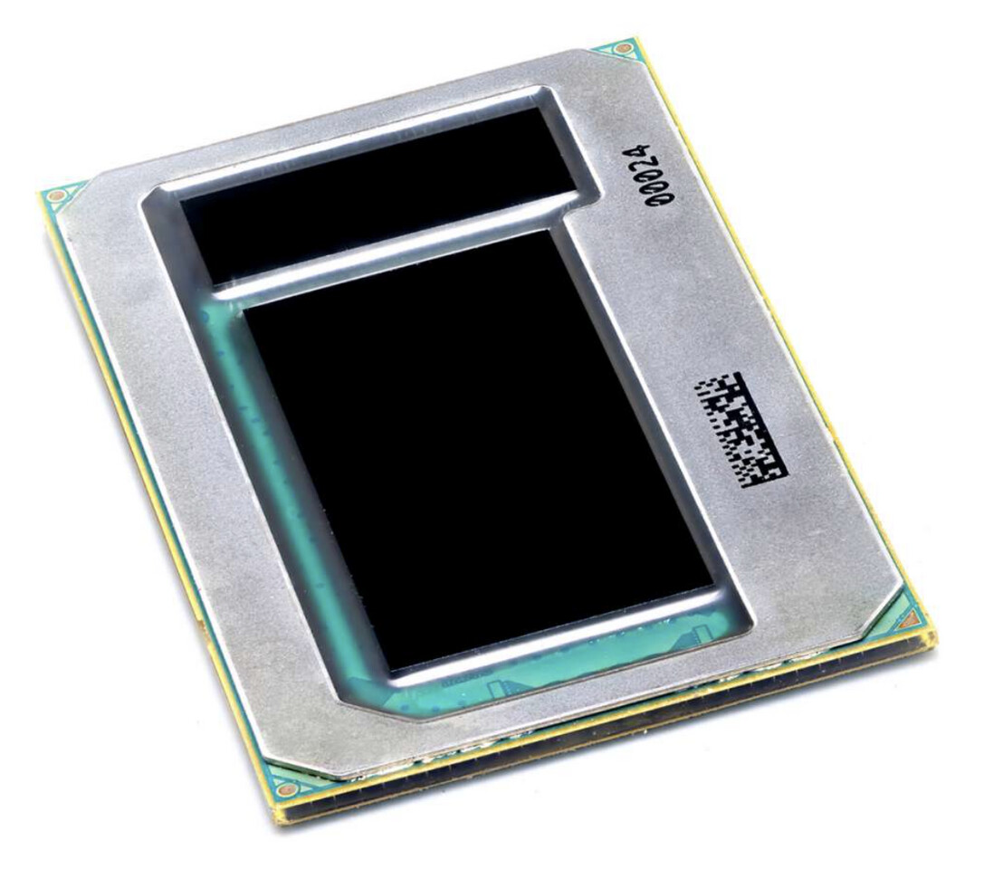
Panther Lake Teardown Shows Intel 18A Near TSMC N3E, Newer TSMC Nodes Still Ahead
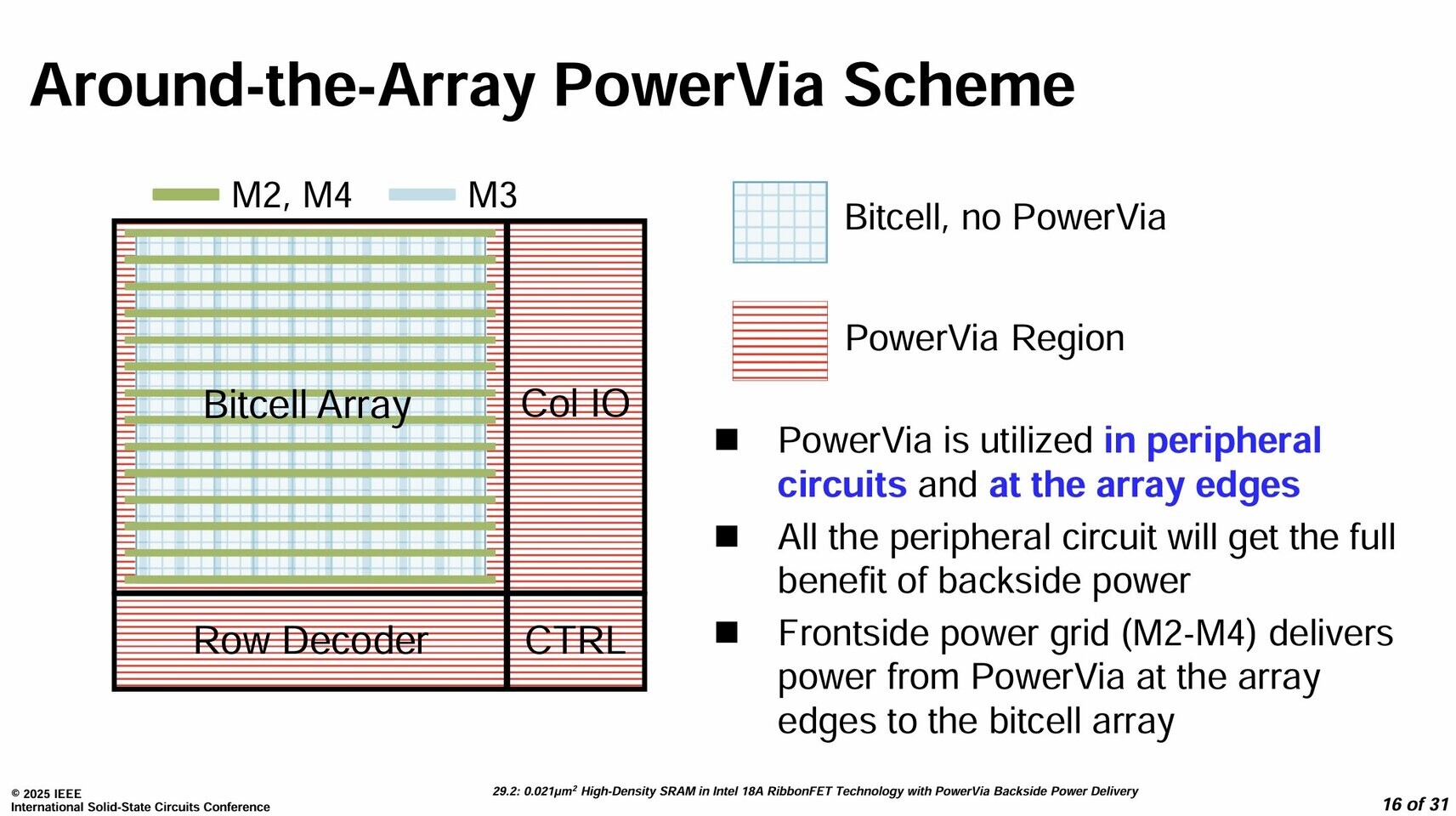
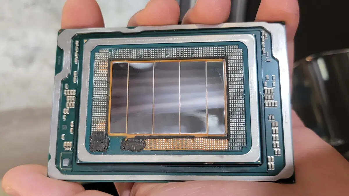
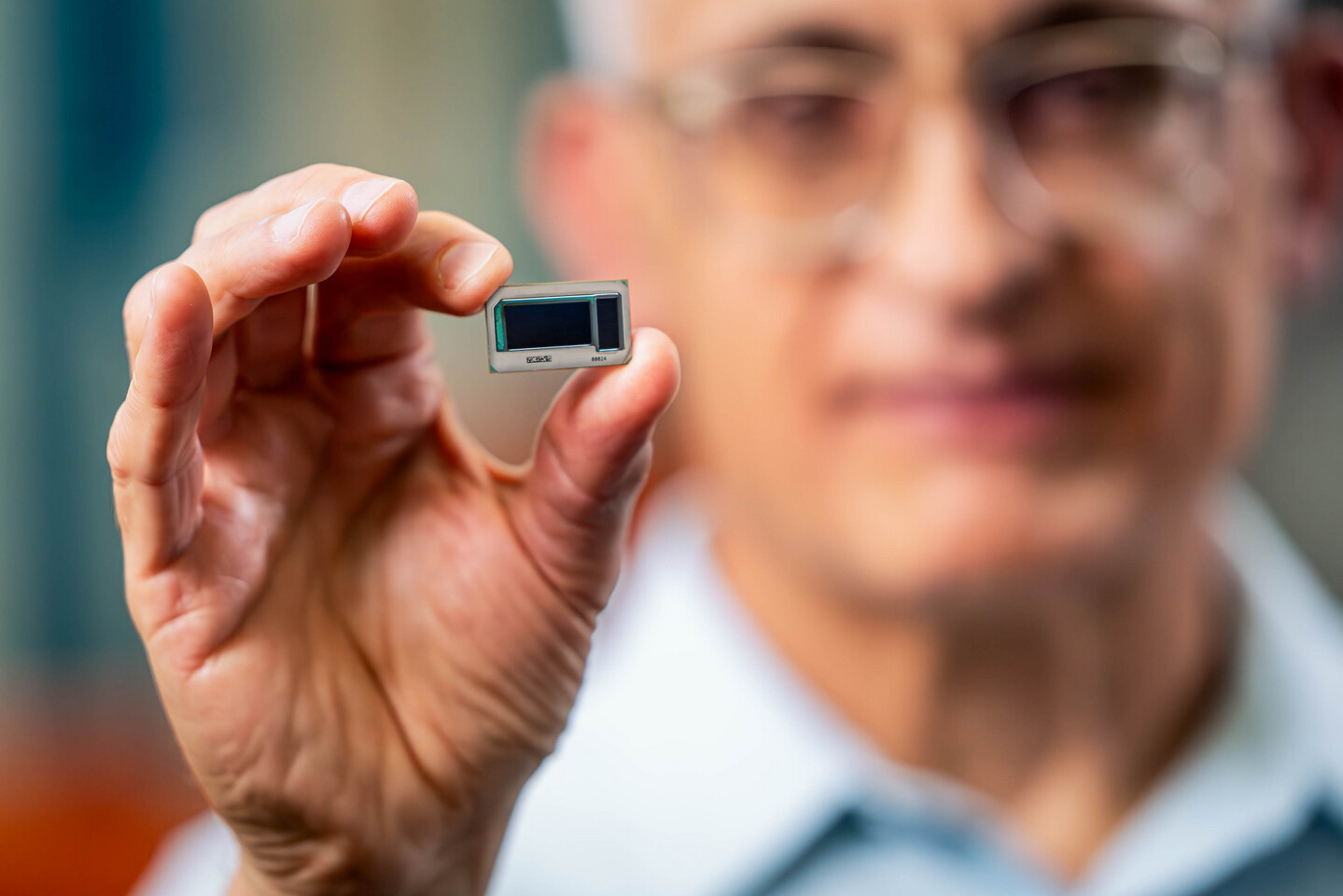
SemiAnalysis has published a teardown of Intel's Panther Lake (Core Ultra 7 365), offering a rare look at 18A inside a shipping chip. Intel's 18A node brings advanced manufacturing technologies such as rear-side power delivery and a new transistor design, so its success is vital for the Foundry. The firm found the 18A compute logic to be similar in density to the TSMC N3E logic used in the 12-core Xe3 GPU tile. It also puts 18A about 18.6% denser than the Intel 3 GPU logic, using a representative-cell model. However, SemiAnalysis says 18A does not lead TSMC N3P, N2, or Samsung SF2 in peak density. It further cautions that whole-die density depends on cell mix and placement.
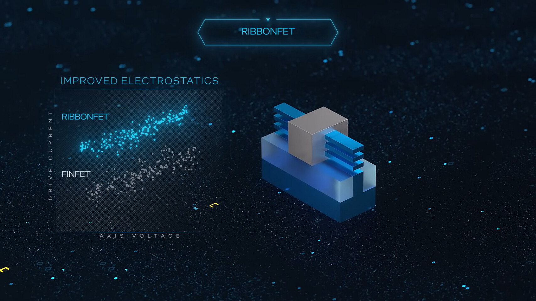
Panther Lake is Intel's first chip with RibbonFET gate-all-around transistors, and the first commercial implementation of PowerVia backside power delivery. SemiAnalysis counted four stacked ribbons per transistor, compared to three sheets on Samsung's SF2. Moreover, the Cougar Cove P-core takes roughly the same area as Lunar Lake's Lion Cove, even though L2 grew from 2.5 MiB to 3 MiB. Panther Lake's NPU 5 reportedly requires 36.9% less chip area than Lunar Lake's NPU 4, though the number of INT8 MAC units remains the same. SemiAnalysis describes the CPU cores as incremental updates.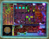
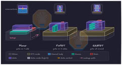
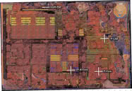
Panther Lake is Intel's first chip with RibbonFET gate-all-around transistors, and the first commercial implementation of PowerVia backside power delivery. SemiAnalysis counted four stacked ribbons per transistor, compared to three sheets on Samsung's SF2. Moreover, the Cougar Cove P-core takes roughly the same area as Lunar Lake's Lion Cove, even though L2 grew from 2.5 MiB to 3 MiB. Panther Lake's NPU 5 reportedly requires 36.9% less chip area than Lunar Lake's NPU 4, though the number of INT8 MAC units remains the same. SemiAnalysis describes the CPU cores as incremental updates.