Sunday, October 26th 2025

Intel's Advanced Packaging Could Be America's Answer to Silicon Dominance
Intel might be the key to re-realizing the American dream of advanced chip production and packaging on U.S. soil. Under the Trump administration, the United States has been making significant efforts to establish leading-edge chip manufacturing domestically. Achieving this goal is challenging for several reasons. In the race for the most advanced silicon, only a few major veteran players remain: Intel, Samsung, and TSMC. Among these, Taiwan-based TSMC has consistently overcome obstacles to become the leader in the semiconductor industry. Through a strategic approach to semiconductor development, TSMC has excelled in both leading-edge node production and advanced chip packaging, enhancing performance.
Historically, Intel has faced difficulties with leading-edge semiconductor node production, even outsourcing some chip manufacturing to TSMC. However, there is a significant opportunity for Intel to not only produce silicon but also establish itself as a major packaging partner for many manufacturers, including TSMC. TSMC's facilities in Arizona address the issue of USA-based manufacturing only partially. While TSMC's Arizona Fab 21 produces 4 nm wafers, these wafers must be sent back to Taiwan for packaging, disrupting the sovereign supply chain that is crucial for domestic manufacturing. Addressing these issues could present a good opportunity for Intel, even if Team Blue doesn't manufacture the underlying silicon.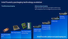

 Traditionally, Intel has relied on its global sites, such as the Pelican plant in Malaysia, for some of its packaging designs. However, starting in early 2024, Intel expanded its New Mexico facilities to accommodate more advanced packaging capabilities, establishing a true independence layer. The Fab 9 and Fab 11x facilities in Rio Rancho are the first to mass-produce Intel's 3D advanced packaging technology. This site is also Intel's first high-volume advanced packaging facility that is co-located, enabling a complete manufacturing process and creating a more efficient supply chain from demand to finished product.
Enter Intel Foundry's Advanced Packaging Services
Intel's Foundry advanced packaging portfolio allows designers to use 2D, 2.5D, and 3D building blocks to optimize cost, power, and bandwidth at the system level. EMIB is a substrate-embedded silicon bridge that provides localized, high-density die-to-die routing without the cost and area penalty of a full-size silicon interposer. For instance, small silicon EMIB bridges—available in variants like EMIB-M with embedded MIM capacitors, and EMIB-T with TSVs—provide low-cost, high-density shoreline connections ideal for logic-to-logic and logic-to-HBM interfaces. Additionally, the Foveros family, including Foveros-S, R, B, and Foveros Direct, offers interposer and RDL options along with true 3D stacking using Cu-to-Cu hybrid bonding, for scenarios requiring extreme die-to-die bandwidth or power efficiency.
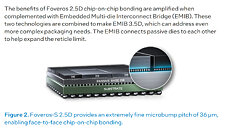
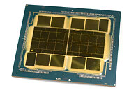
These variants of EMIB are giving flexibility to every chip designer, depending on the type of package. Overcoming the full reticle size of 830 mm² is possible with the use of EMIB, so ASIC designers can choose designs that are as complex as Intel's "Ponte Vecchio," which uses EMIB 3.5D for more than 100 billion transistors, 47 active tiles, and five process nodes combined on a single chip. The sheer complexity of this product—powering the Exascale supercomputer Aurora—demonstrated that Intel was able to deliver a product with the world's most advanced packaging in a mission-critical environment. This proved that advanced packaging stores a completely separate value inside Intel Foundry.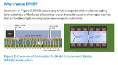
 On the topic of silicon, Intel's 18A node and its future variations, 18A-P and 18A-PT, are going to be long-lived nodes inside Intel facilities. At the recent Q3 earnings call, CFO David Zinsner stated: "We are not at peak supply for 18A. In fact, we don't get there until the end of the decade. We do think that this node will be a fairly long-lived node for us. We will continue to make investments on 18A over time." This continued investment will drive yield, as well as variations of the 18A node adapted for designs from mobile to HPC and AI. This demonstrates that Intel has strategically invested over the years to ensure sufficient capacity. Even with the addition of new customers, there will still be enough 18A wafer supply to meet Intel's own product portfolio goals while also providing a reliable supply for external customers.
However, a real advantage for Intel nodes begins with 14A, which is industry's first High-NA EUV design. Intel has reported processing over 30,000 wafers in a single quarter using High-NA EUV exposure, achieving simplified manufacturing by reducing the required steps for a particular layer from 40 to fewer than 10, which has led to faster cycle times. Additionally, at this stage of development, 14A is reaching better milestones than 18A. This has been done in coordination with external partners to ensure that when the 14A node goes into volume production, everything will be ready for smooth integration and manufacturing.
Completing the entire semiconductor manufacturing process is a complex task. Although TSMC can provide advanced—but not its most advanced—manufacturing capabilities in the USA, packaging remains a challenge. To address this, TSMC plans to collaborate with Amkor, which is constructing a $7 billion facility in Arizona focused on advanced outsourced semiconductor packaging and testing. This partnership will enable TSMC to outsource packaging to Amkor's Arizona facility, allowing chips produced at the nearby TSMC Fab 21 to be packaged there. Amkor aims to finish the new site by mid-2027, with production set to begin in early 2028. In the meantime, Intel can offer its advanced EMIB packaging to partners, even TSMC's customers, who could be using these advanced packaging techniques to build a competitive product. The only question that remains is how far is Intel willing to push its external packaging business, without obliging customers to its 18A and 14A nodes.
Historically, Intel has faced difficulties with leading-edge semiconductor node production, even outsourcing some chip manufacturing to TSMC. However, there is a significant opportunity for Intel to not only produce silicon but also establish itself as a major packaging partner for many manufacturers, including TSMC. TSMC's facilities in Arizona address the issue of USA-based manufacturing only partially. While TSMC's Arizona Fab 21 produces 4 nm wafers, these wafers must be sent back to Taiwan for packaging, disrupting the sovereign supply chain that is crucial for domestic manufacturing. Addressing these issues could present a good opportunity for Intel, even if Team Blue doesn't manufacture the underlying silicon.


Enter Intel Foundry's Advanced Packaging Services
Intel's Foundry advanced packaging portfolio allows designers to use 2D, 2.5D, and 3D building blocks to optimize cost, power, and bandwidth at the system level. EMIB is a substrate-embedded silicon bridge that provides localized, high-density die-to-die routing without the cost and area penalty of a full-size silicon interposer. For instance, small silicon EMIB bridges—available in variants like EMIB-M with embedded MIM capacitors, and EMIB-T with TSVs—provide low-cost, high-density shoreline connections ideal for logic-to-logic and logic-to-HBM interfaces. Additionally, the Foveros family, including Foveros-S, R, B, and Foveros Direct, offers interposer and RDL options along with true 3D stacking using Cu-to-Cu hybrid bonding, for scenarios requiring extreme die-to-die bandwidth or power efficiency.
These variants of EMIB are giving flexibility to every chip designer, depending on the type of package. Overcoming the full reticle size of 830 mm² is possible with the use of EMIB, so ASIC designers can choose designs that are as complex as Intel's "Ponte Vecchio," which uses EMIB 3.5D for more than 100 billion transistors, 47 active tiles, and five process nodes combined on a single chip. The sheer complexity of this product—powering the Exascale supercomputer Aurora—demonstrated that Intel was able to deliver a product with the world's most advanced packaging in a mission-critical environment. This proved that advanced packaging stores a completely separate value inside Intel Foundry.


However, a real advantage for Intel nodes begins with 14A, which is industry's first High-NA EUV design. Intel has reported processing over 30,000 wafers in a single quarter using High-NA EUV exposure, achieving simplified manufacturing by reducing the required steps for a particular layer from 40 to fewer than 10, which has led to faster cycle times. Additionally, at this stage of development, 14A is reaching better milestones than 18A. This has been done in coordination with external partners to ensure that when the 14A node goes into volume production, everything will be ready for smooth integration and manufacturing.
Completing the entire semiconductor manufacturing process is a complex task. Although TSMC can provide advanced—but not its most advanced—manufacturing capabilities in the USA, packaging remains a challenge. To address this, TSMC plans to collaborate with Amkor, which is constructing a $7 billion facility in Arizona focused on advanced outsourced semiconductor packaging and testing. This partnership will enable TSMC to outsource packaging to Amkor's Arizona facility, allowing chips produced at the nearby TSMC Fab 21 to be packaged there. Amkor aims to finish the new site by mid-2027, with production set to begin in early 2028. In the meantime, Intel can offer its advanced EMIB packaging to partners, even TSMC's customers, who could be using these advanced packaging techniques to build a competitive product. The only question that remains is how far is Intel willing to push its external packaging business, without obliging customers to its 18A and 14A nodes.
25 Comments on Intel's Advanced Packaging Could Be America's Answer to Silicon Dominance
Its hot, dusty, water seems to be scarce.. being in a desert and all..?
What the actual eff?
Do we really wanna repeat that?
Plus once you build somewhere and all the surrounding infrastructure is built - supply chains, talent, utilities, housing, education, etc. it’s a hell of a lot cheaper to expand in the area than to rebuild that all somewhere else.
In that paradigm, suddenly a desert where no civilians 'need' water to live, seems like an opportunity.
It only goes to show how far we have regressed in our search for habitable land for what we 'need'...
Canada has everything to make chips.
Would be perfect for Data Centers too, since we have a ton of power, and a cool climate for 2/3 of the year.
But your most important factor is labor, like a fab you still need lots of mechanical and chemical engineers. These guys operate the machines or maintain the automated systems that do work too fine for anyone to do literally by hand. Without them the packaging facility is just die storage. But to do their job they still need TONS of people specialized in robotics and machine vision, to keep the machines running, and often overlooked is maintenance folks that are tasked with doing ANYTHING they can in-house to keep those machines running, or getting specialists involved from the companies they bought the machines from. This is all high skill labor regardless of the pay. So having your packaging near the fabs and companies that support them keeps you in an industry pool that sees people cycle in and out to different positions.
The other big demands in no particular order would be power stability, ESD control/clean room environments, and your supply chain/logistics. Power is big, you cant have high precision automated equipment dealing with power spikes and outages. All those ovens and HVAC systems consume a lot of power, but stable power is key. That may mean new power facilities and theres all kinds of zoning and regulation the closer to you get to major populations or their resources. Arizona is good for that, they have a stable grid and a willingness to zone around the needs of the semiconductor industry specifically. TSMC chose arizona for that reason, back home the government supports semicondutors. If they need financing, zoning, regulation, infractsucture, universities...it happens.
Vibration tolerance matters, but its a smaller issue in packaging than when you're in lithography stages. You're usually more worried about the power going out than you are about an earth quake in this stage. Other factors you'd want on your list is water quality (not just quantity as filtering is expensive) as well as your chemical logistics, storage and safety. You use a lot of chemicals and though its less than in lithography, you need a way to treat, store, and process these and it helps if theres nothing near by you can contaminate in a meaningfully "oh shit" moment. This is stuff like epoxies, curing agents, hardeners, fluxes, solder pastes, etchant chemicals, acids, and stuff you want to isolate. The supply of these is also something you want to consider, as the shorter the trip you need to take with toxic chemicals, the better it is for everyone else.
So really, the things that make Arizona a bad place for packaging - dry air isnt good for static and dust is bad as a contaminate..but you can build around that. If the energy costs go up due to that or HVAC needing to manage the internal climate in a desert, you can reclaim a lot of that cost with solar panels on the roof that take advantage of that Arizona sun. But logistics and labor are probably why youd put it here. Lots of skilled labor in the area due to the fabs in AZ from Intel & TSMC, NXP has wafer production and research there, and though Microchip Semi just closed their wafer fabs in AZ in 23/24, that expertiese and knowledge went somewhere local id bet. The companies that provide your specility gassses, chiemicals (and their distro), providers of your ultra pure water, and solvents..these guys are also going to be in AZ servicing the industry.
so putting it anywhere else to take advantage of some local factor, cant overlook the others. Cheap power and tons of clean water on stable ground gets you in the conversation, but not across the finishline. You need a shit load of people in supporting industries, and it helps if they are already near by or could be incentivised to be near by.
www.servethehome.com/intel-fab-52-in-chandler-arizona-is-running-18a/
Patrick Kennedy in that article said,
www.google.com/search?q=lake+meed&sca_esv=8e61a810906f0d86&udm=2&biw=2552&bih=1314&ei=9s3-aJfNJti3ptQPl8b72AY&ved=0ahUKEwiXoIKSoMOQAxXYm4kEHRfjHmsQ4dUDCBI&uact=5&oq=lake+meed&gs_lp=Egtnd3Mtd2l6LWltZyIJbGFrZSBtZWVkMg0QABiABBixAxhDGIoFMgoQABiABBhDGIoFMg0QABiABBixAxhDGIoFMgoQABiABBhDGIoFMgcQABiABBgKMgcQABiABBgKMgcQABiABBgKMgcQABiABBgKMgcQABiABBgKMgcQABiABBgKSO4OUABYlw1wAHgAkAEAmAFcoAG8BaoBATm4AQPIAQD4AQGYAgmgAssFwgIIEAAYgAQYsQPCAgsQABiABBixAxiDAcICBRAAGIAEwgIEEAAYA5gDAJIHATmgB50wsgcBObgHywXCBwMwLjnIBws&sclient=gws-wiz-img
www.planetizen.com/news/2025/10/136234-arizona-overrides-moratorium-imposed-due-water-crisis-approves-60k-new-homes
The moratorium requires renewable water (not groundwater sourced) be brought in to any new housing (in affected areas).
Arizona does have a water problem and it requires conservation action, regulations and a long-term plan (which are all great things to do). This USGS site has more info.
We've already seen that TSMC got an equivalent to any packaging tech that Intel is developing. It's just that the new tech will be Taiwan first, US second. If Intel sleeps, the industry will just go right back to TSMC.
Maybe someday we’ll have some kind of interconnected network that has searchable databases containing information like this.
If you care to look at some of the other editorials I've made:
www.techpowerup.com/265303/x86-lacks-innovation-arm-is-catching-up-enough-to-replace-the-giant
I usually do weeks of observation, reading, and research before doing anything "speculative" :)